19N10G-TM3-T. Аналоги и основные параметры
Наименование производителя: 19N10G-TM3-T
Тип транзистора: MOSFET
Полярность: N
Предельные значения
Pd ⓘ
- Максимальная рассеиваемая мощность: 50 W
|Vds|ⓘ - Максимально допустимое напряжение сток-исток: 100 V
|Vgs|ⓘ - Максимально допустимое напряжение затвор-исток: 25 V
|Id| ⓘ - Максимально допустимый постоянный ток стока: 15.6 A
Tj ⓘ - Максимальная температура канала: 150 °C
Электрические характеристики
tr ⓘ -
Время нарастания: 70 ns
Cossⓘ - Выходная емкость: 165 pf
RDSonⓘ - Сопротивление сток-исток открытого транзистора: 0.1 Ohm
Тип корпуса: TO-251
Аналог (замена) для 19N10G-TM3-T
- подборⓘ MOSFET транзистора по параметрам
19N10G-TM3-T даташит
9.1. Size:611K fairchild semi
fqb19n10ltm.pdf 
August 2000 TM QFET QFET QFET QFET FQB19N10L / FQI19N10L 100V LOGIC N-Channel MOSFET General Description Features These N-Channel enhancement mode power field effect 19A, 100V, RDS(on) = 0.1 @VGS = 10 V transistors are produced using Fairchild s proprietary, Low gate charge ( typical 14 nC) planar stripe, DMOS technology. Low Crss ( typical 35 pF) This advanced tec
9.2. Size:581K fairchild semi
fqpf19n10.pdf 
August 2000 TM QFET QFET QFET QFET FQPF19N10 100V N-Channel MOSFET General Description Features These N-Channel enhancement mode power field effect 13.6A, 100V, RDS(on) = 0.1 @VGS = 10 V transistors are produced using Fairchild s proprietary, Low gate charge ( typical 19 nC) planar stripe, DMOS technology. Low Crss ( typical 32 pF) This advanced technology has been
9.3. Size:626K fairchild semi
fqp19n10l.pdf 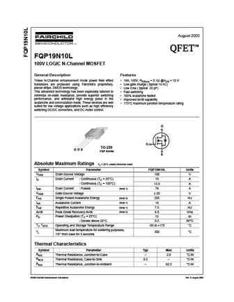
August 2000 TM QFET QFET QFET QFET FQP19N10L 100V LOGIC N-Channel MOSFET General Description Features These N-Channel enhancement mode power field effect 19A, 100V, RDS(on) = 0.1 @VGS = 10 V transistors are produced using Fairchild s proprietary, Low gate charge ( typical 14 nC) planar stripe, DMOS technology. Low Crss ( typical 35 pF) This advanced technology has
9.4. Size:591K fairchild semi
fqp19n10.pdf 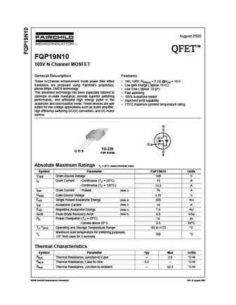
August 2000 TM QFET QFET QFET QFET FQP19N10 100V N-Channel MOSFET General Description Features These N-Channel enhancement mode power field effect 19A, 100V, RDS(on) = 0.1 @VGS = 10 V transistors are produced using Fairchild s proprietary, Low gate charge ( typical 19 nC) planar stripe, DMOS technology. Low Crss ( typical 32 pF) This advanced technology has been es
9.5. Size:688K fairchild semi
fqd19n10ltf fqd19n10ltm fqd19n10l fqu19n10l.pdf 
January 2009 QFET FQD19N10L / FQU19N10L 100V LOGIC N-Channel MOSFET General Description Features These N-Channel enhancement mode power field effect 15.6A, 100V, RDS(on) = 0.1 @VGS = 10 V transistors are produced using Fairchild s proprietary, Low gate charge ( typical 14 nC) planar stripe, DMOS technology. Low Crss ( typical 35 pF) This advanced technology has been
9.6. Size:678K fairchild semi
fqd19n10tf fqd19n10tm fqd19n10 fqu19n10.pdf 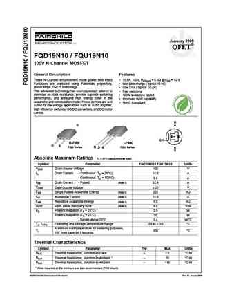
January 2009 QFET FQD19N10 / FQU19N10 100V N-Channel MOSFET General Description Features These N-Channel enhancement mode power field effect 15.6A, 100V, RDS(on) = 0.1 @VGS = 10 V transistors are produced using Fairchild s proprietary, Low gate charge ( typical 19 nC) planar stripe, DMOS technology. Low Crss ( typical 32 pF) This advanced technology has been especial
9.7. Size:926K fairchild semi
fqb19n10tm.pdf 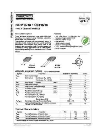
October 2008 QFET FQB19N10 / FQI19N10 100V N-Channel MOSFET General Description Features These N-Channel enhancement mode power field effect 19A, 100V, RDS(on) = 0.1 @VGS = 10 V transistors are produced using Fairchild s proprietary, Low gate charge ( typical 19 nC) planar stripe, DMOS technology. Low Crss ( typical 32 pF) This advanced technology has been especially
9.8. Size:616K fairchild semi
fqpf19n10l.pdf 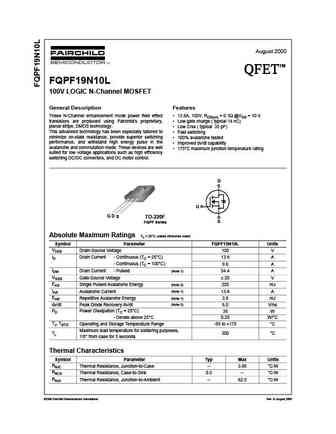
August 2000 TM QFET QFET QFET QFET FQPF19N10L 100V LOGIC N-Channel MOSFET General Description Features These N-Channel enhancement mode power field effect 13.6A, 100V, RDS(on) = 0.1 @VGS = 10 V transistors are produced using Fairchild s proprietary, Low gate charge ( typical 14 nC) planar stripe, DMOS technology. Low Crss ( typical 35 pF) This advanced technology h
9.9. Size:246K utc
19n10.pdf 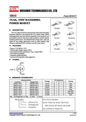
UNISONIC TECHNOLOGIES CO., LTD 19N10 Power MOSFET 15.6A, 100V N-CHANNEL POWER MOSFET DESCRIPTION The UTC 100V N-Channel enhancement mode power field effect transistors (MOSFET) are produced by UTC s planar stripe, DMOS technology which has been tailored especially in the avalanche and commutation mode to minimize on-state resistance, provide superior switching performance
9.10. Size:882K ncepower
ncep019n10t.pdf 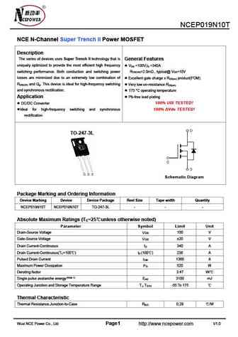
NCEP019N10T NCE N-Channel Super Trench II Power MOSFET Description The series of devices uses Super Trench II technology that is General Features uniquely optimized to provide the most efficient high frequency V =100V,I =340A DS D switching performance. Both conduction and switching power R =2.0m , typical@ V =10V DS(ON) GS losses are minimized due to an extremely low combinatio
9.11. Size:636K samwin
swp19n10 swd19n10 swi19n10.pdf 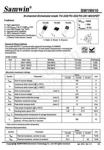
SW19N10 N-channel Enhanced mode TO-220/TO-252/TO-251 MOSFET Features BVDSS 100V TO-220 TO-252 TO-251 ID 19A High ruggedness Low RDS(ON) (Typ 0.1 )@VGS=10V RDS(ON) 0.1 Low Gate Charge (Typ 15nC) Improved dv/dt Capability 100% Avalanche Tested 1 1 1 2 2 2 2 Application Synchronous Rectification, 3 3 3 Li Battery Protect Boa
9.12. Size:501K way-on
wmq119n10lg2.pdf 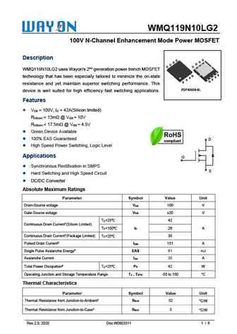
WMQ119N10LG2 100V N-Channel Enhancement Mode Power MOSFET Description D D D D D D D D WMQ119N10LG2 uses Wayon's 2nd generation power trench MOSFET S G technology that has been especially tailored to minimize the on-state S S S S G S resistance and yet maintain superior switching performance. This PDFN3030-8L device is well suited for high efficiency fast switching ap
9.13. Size:790K way-on
wmp119n10lg2.pdf 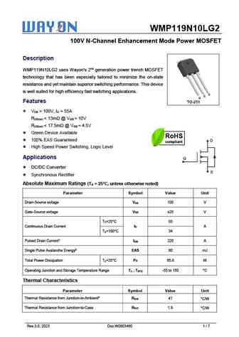
WMP119N10LG2 100V N-Channel Enhancement Mode Power MOSFET Description WMP119N10LG2 uses Wayon's 2nd generation power trench MOSFET technology that has been especially tailored to minimize the on-state resistance and yet maintain superior switching performance. This device is well suited for high efficiency fast switching applications. Features V = 100V, I = 55A DS D R
9.14. Size:519K way-on
wmb119n10lg2.pdf 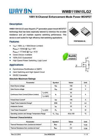
WMB119N10LG2 100V N-Channel Enhancement Mode Power MOSFET Description D D D WMB119N10LG2 uses Wayon's 2nd generation power trench MOSFET DD D D D technology that has been especially tailored to minimize the on-state G ss resistance and yet maintain superior switching performance. This s ss G s device is well suited for high efficiency fast switching applications. PDFN50
9.16. Size:884K cn vbsemi
fqd19n10l.pdf 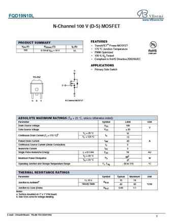
FQD19N10L www.VBsemi.tw N-Channel 100 V (D-S) MOSFET FEATURES PRODUCT SUMMARY TrenchFET Power MOSFET VDS (V) RDS(on) ( )ID (A) 175 C Junction Temperature 100 0.11 4 at VGS = 10 V 15 PWM Optimized 100 % Rg Tested Compliant to RoHS Directive 2002/95/EC APPLICATIONS Primary Side Switch D TO-252 G S G D S N-Channel MOSFET ABSOLUTE MAXIMUM RATINGS
Другие IGBT... 19N10G-T3P-T, 19N10L-TA3-T, 19N10G-TA3-T, 19N10L-TF3-T, 19N10G-TF3-T, 19N10L-TF1-T, 19N10G-TF1-T, 19N10L-TM3-T, IRF530, 19N10L-TMS-T, 19N10L-TMS2-T, 19N10G-TMS2-T, 19N10L-TMS4-T, 19N10G-TMS4-T, 19N10L-TN3-R, 19N10G-TN3-R, 19N10L-TQ2-R