25N10L-TF2-T. Аналоги и основные параметры
Наименование производителя: 25N10L-TF2-T
Тип транзистора: MOSFET
Полярность: N
Предельные значения
Pd ⓘ - Максимальная рассеиваемая мощность: 52 W
|Vds|ⓘ - Максимально допустимое напряжение сток-исток: 100 V
|Vgs|ⓘ - Максимально допустимое напряжение затвор-исток: 20 V
|Id| ⓘ - Максимально допустимый постоянный ток стока: 23 A
Tj ⓘ - Максимальная температура канала: 150 °C
Электрические характеристики
tr ⓘ - Время нарастания: 28 ns
Cossⓘ - Выходная емкость: 270 pf
RDSonⓘ - Сопротивление сток-исток открытого транзистора: 0.08 Ohm
Тип корпуса: TO-220F
Аналог (замена) для 25N10L-TF2-T
- подборⓘ MOSFET транзистора по параметрам
25N10L-TF2-T даташит
25n10l-tf1-t 25n10g-tf1-t 25n10l-tf2-t 25n10g-tf2-t 25n10l-tf3-t 25n10g-tf3-t 25n10l-tm3-t 25n10g-tm3-t 25n10l-tn3-r 25n10g-tn3-r.pdf
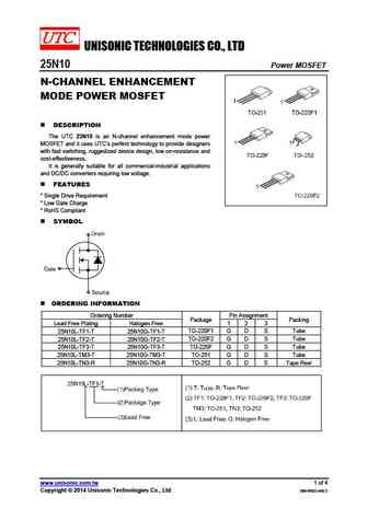
UNISONIC TECHNOLOGIES CO., LTD 25N10 Power MOSFET N-CHANNEL ENHANCEMENT MODE POWER MOSFET DESCRIPTION The UTC 25N10 is an N-channel enhancement mode power MOSFET and it uses UTC s perfect technology to provide designers with fast switching, ruggedized device design, low on-resistance and cost-effectiveness. It is generally suitable for all commercial-industrial applicati
std25n10f7 stf25n10f7 stp25n10f7.pdf
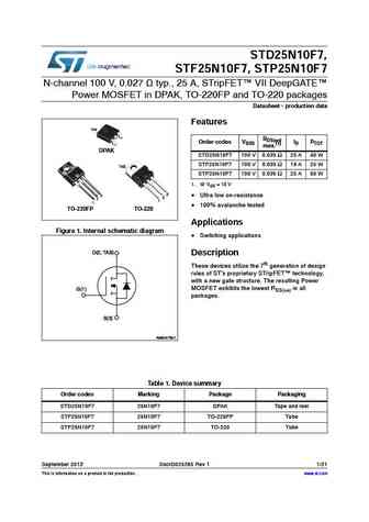
STD25N10F7, STF25N10F7, STP25N10F7 N-channel 100 V, 0.027 typ., 25 A, STripFET VII DeepGATE Power MOSFET in DPAK, TO-220FP and TO-220 packages Datasheet - production data Features TAB RDS(on) Order codes VDSS ID PTOT max.(1) DPAK STD25N10F7 100 V 0.035 25 A 40 W STF25N10F7 100 V 0.035 19 A 25 W TAB STP25N10F7 100 V 0.035 25 A 50 W 1. @ VGS = 10 V 3 3
ipb025n10n3g ipb025n10n3g3.pdf
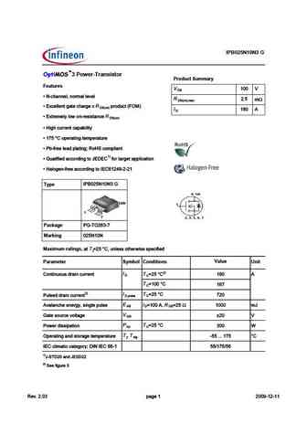
IPB025N10N3 G 3 Power-Transistor Product Summary Features V 1 D P ' 381>>5?A=1
ixgh25n100u1.pdf
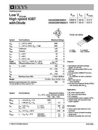
Preliminary data VCES IC25 VCE(sat) Low VCE(sat) High speed IGBT IXGH25N100U1 1000 V 50 A 3.5 V IXGH25N100AU1 1000 V 50 A 4.0 V with Diode TO-247 AD (IXGH) Symbol Test Conditions Maximum Ratings VCES TJ = 25 C to 150 C 1000 V G C E VCGR TJ = 25 C to 150 C; RGE = 1 M 1000 V VGES Continuous 20 V G = Gate C = Collector VGEM Transient 30 V E = Emitter TAB = Collector I
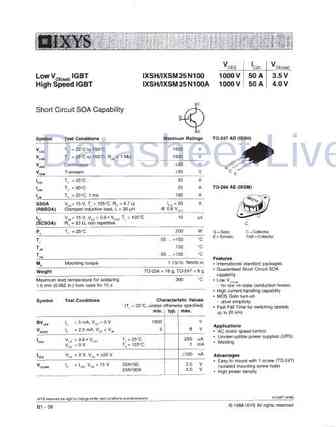
ixgm25n100.pdf

VCES IC25 VCE(sat) Low VCE(sat) IXGH/IXGM 25 N100 1000 V 50 A 3.5 V High speed IGBT IXGH/IXGM 25 N100A 1000 V 50 A 4.0 V Symbol Test Conditions Maximum Ratings TO-247 AD (IXGH) VCES TJ = 25 C to 150 C 1000 V VCGR TJ = 25 C to 150 C; RGE = 1 M 1000 V VGES Continuous 20 V G C VGEM Transient 30 V E IC25 TC = 25 C50 A IC90 TC = 90 C25 A TO-204 AE (IXGM) ICM TC = 25 C, 1 m
ixgh25n100au1.pdf

Preliminary data VCES IC25 VCE(sat) Low VCE(sat) High speed IGBT IXGH25N100U1 1000 V 50 A 3.5 V IXGH25N100AU1 1000 V 50 A 4.0 V with Diode TO-247 AD (IXGH) Symbol Test Conditions Maximum Ratings VCES TJ = 25 C to 150 C 1000 V G C E VCGR TJ = 25 C to 150 C; RGE = 1 M 1000 V VGES Continuous 20 V G = Gate C = Collector VGEM Transient 30 V E = Emitter TAB = Collector I
ixgm25n100a.pdf

VCES IC25 VCE(sat) Low VCE(sat) IXGH/IXGM 25 N100 1000 V 50 A 3.5 V High speed IGBT IXGH/IXGM 25 N100A 1000 V 50 A 4.0 V Symbol Test Conditions Maximum Ratings TO-247 AD (IXGH) VCES TJ = 25 C to 150 C 1000 V VCGR TJ = 25 C to 150 C; RGE = 1 M 1000 V VGES Continuous 20 V G C VGEM Transient 30 V E IC25 TC = 25 C50 A IC90 TC = 90 C25 A TO-204 AE (IXGM) ICM TC = 25 C, 1 m
ixgh25n100a.pdf
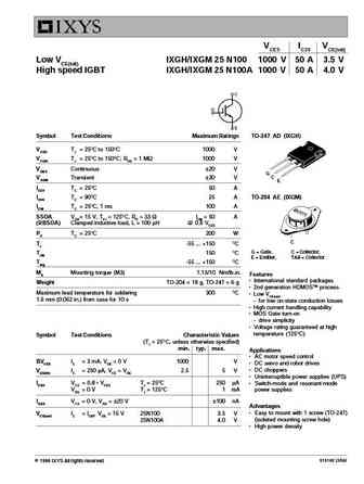
VCES IC25 VCE(sat) Low VCE(sat) IXGH/IXGM 25 N100 1000 V 50 A 3.5 V High speed IGBT IXGH/IXGM 25 N100A 1000 V 50 A 4.0 V Symbol Test Conditions Maximum Ratings TO-247 AD (IXGH) VCES TJ = 25 C to 150 C 1000 V VCGR TJ = 25 C to 150 C; RGE = 1 M 1000 V VGES Continuous 20 V G C VGEM Transient 30 V E IC25 TC = 25 C50 A IC90 TC = 90 C25 A TO-204 AE (IXGM) ICM TC = 25 C, 1 m
ixgh25n100.pdf

VCES IC25 VCE(sat) Low VCE(sat) IXGH/IXGM 25 N100 1000 V 50 A 3.5 V High speed IGBT IXGH/IXGM 25 N100A 1000 V 50 A 4.0 V Symbol Test Conditions Maximum Ratings TO-247 AD (IXGH) VCES TJ = 25 C to 150 C 1000 V VCGR TJ = 25 C to 150 C; RGE = 1 M 1000 V VGES Continuous 20 V G C VGEM Transient 30 V E IC25 TC = 25 C50 A IC90 TC = 90 C25 A TO-204 AE (IXGM) ICM TC = 25 C, 1 m
25n10.pdf

UNISONIC TECHNOLOGIES CO., LTD 25N10 Power MOSFET N-CHANNEL ENHANCEMENT MODE POWER MOSFET DESCRIPTION The UTC 25N10 is an N-channel enhancement mode power MOSFET and it uses UTC s perfect technology to provide designers with fast switching, ruggedized device design, low on-resistance and cost-effectiveness. It is generally suitable for all commercial-industrial applicati
ap25n10gh.pdf
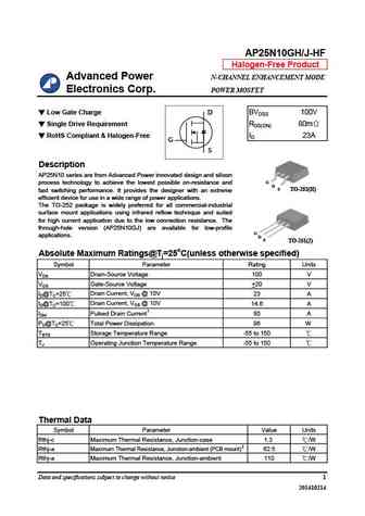
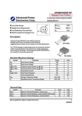
AP25N10GH/J-HF Halogen-Free Product Advanced Power N-CHANNEL ENHANCEMENT MODE Electronics Corp. POWER MOSFET Low Gate Charge D BVDSS 100V Single Drive Requirement RDS(ON) 80m RoHS Compliant & Halogen-Free ID 23A G S Description AP25N10 series are from Advanced Power innovated design and silicon G process technology to achieve the lowest possible on-resistance and D S
ap25n10gp-hf ap25n10gs-hf.pdf
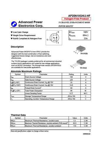
AP25N10GS/P-HF Halogen-Free Product Advanced Power N-CHANNEL ENHANCEMENT MODE Electronics Corp. POWER MOSFET D Low Gate Charge BVDSS 100V Simple Drive Requirement RDS(ON) 80m Fast Switching Characteristic ID 23A G RoHS Compliant & Halogen-Free S Description Advanced Power MOSFETs from APEC provide the designer with the best combination of fast switching, G TO-220
ap25n10gh-hf ap25n10gj-hf.pdf
AP25N10GH/J-HF Halogen-Free Product Advanced Power N-CHANNEL ENHANCEMENT MODE Electronics Corp. POWER MOSFET Low Gate Charge D BVDSS 100V Single Drive Requirement RDS(ON) 80m RoHS Compliant & Halogen-Free ID 23A G S Description G Advanced Power MOSFETs from APEC provide the D S TO-252(H) designer with the best combination of fast switching, ruggedized device design
gt125n10t gt125n10m gt125n10f.pdf
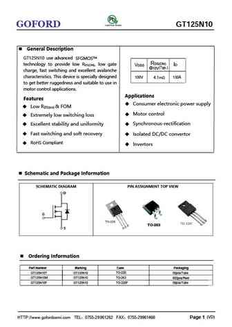
GT125N10 GOFORD General Description GT125N10 use advanced SFGMOSTM RDS(ON) technology to provide low R , low gate DS(ON) VDSS ID @10V (Typ.) charge, fast switching and excellent avalanche characteristics. This device is specially designed 100V 130 A 4.1m to get better ruggedness and suitable to use in motor control applications. Applications Features Consu
25n10 f25n10 i25n10 e25n10 b25n10 d25n10.pdf
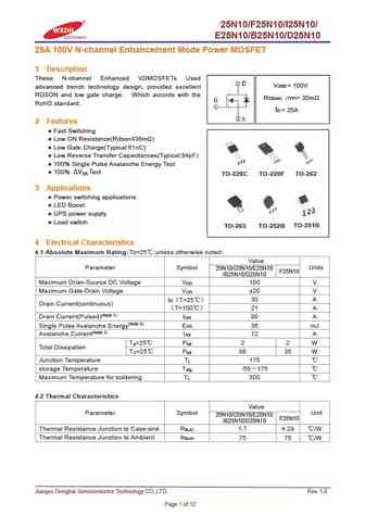
25N10/F25N10/I25N10/ E25N10/B25N10/D25N10 25A 100V N-channel Enhancement Mode Power MOSFET 1 Description These N-channel Enhanced VDMOSFETs Used V = 100V DSS advanced trench technology design, provided excellent RDSON and low gate charge. Which accords with the R = 30m DS(on) TYP) RoHS standard. I = 25A D 2 Features Fast Switching Low ON Resistance(Rdson 36m )
dhs025n10 dhs025n10e dhs025n10d dhs025n10b.pdf
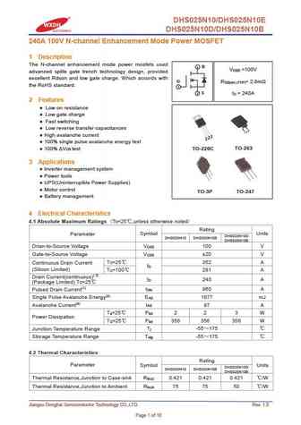
DHS025N10/DHS025N10E DHS025N10D/DHS025N10B 240A 100V N-channel Enhancement Mode Power MOSFET 1 Description The N-channel enhancement mode power mosfets used 2 D V =100V DSS advanced splite gate trench technology design, provided excellent Rdson and low gate charge. Which accords with G R = 2.8m DS(on) (TYP) the RoHS standard. 1 3 S I = 240A D 2 Features Low on resistanc
dhs025n10u.pdf
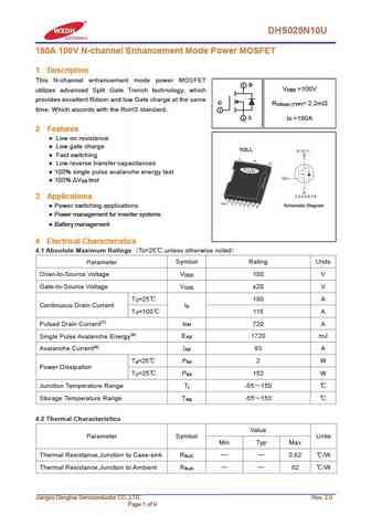
DHS025N10U 180A 100V N-channel Enhancement Mode Power MOSFET 1 Description This N-channel enhancement mode power MOSFET 2 D V =100V DSS utilizes advanced Split Gate Trench technology, which provides excellent Rdson and low Gate charge at the same G R = 2.2m DS(on) (TYP) time. Which accords with the RoHS standard. 1 3 S I =180A D 2 Features Low on resistance Low gate
blp025n10-b blp025n10-p.pdf
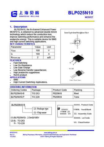
BLP025N10 MOSFET Step-Down Converter 1 Description , BLP025N10, the N-channel Enhanced Power MOSFETs, is obtained by advanced double trench technology which reduce the conduction loss, improve switching performance and enhance the avalanche energy. This is suitable device for BMS and high current switching applications. KEY CHARACTERISTICS Parameter Value Unit V 10
hy125n10t.pdf
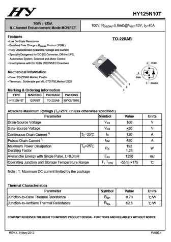
SINGLE FIG.SINGLE PHASE HALF WAVE 60Hz DERATING CURVE FIG. 2 MAXIMUM NON- T1 FORWARD CURRENT AMBIENT TEMPERATURE ( ) 1 2 5 10 1 25 50 75 10 20 150 175 0.00 0.2 0.4 0.6 4 100 125 100 HY125N10T 100V / 125A 100V, RDS(ON)=5.8mW@VGS=10V, ID=40A N-Channel Enhancement Mode MOSFET Features TO-220AB Low On-State Resistance Excellent Gate Charge x RDS(ON) Product
ncep25n10ad.pdf
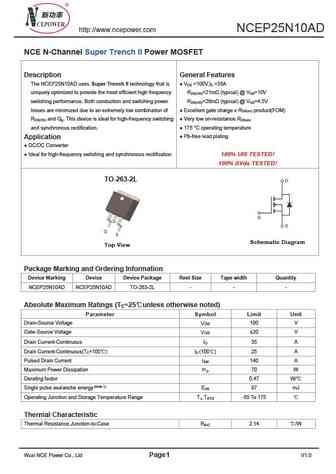
http //www.ncepower.com NCEP25N10AD NCE N-Channel Super Trench II Power MOSFET Description General Features The NCEP25N10AD uses Super Trench II technology that is V =100V,I =35A DS D uniquely optimized to provide the most efficient high frequency R =21m (typical) @ V =10V DS(ON) GS switching performance. Both conduction and switching power R =26m (typical) @ V =4.5V DS(ON) GS
nceap25n10ak.pdf
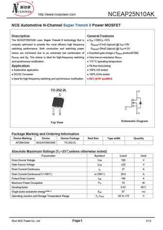
http //www.ncepower.com NCEAP25N10AK NCE Automotive N-Channel Super Trench II Power MOSFET Description General Features The NCEAP25N10AK uses Super Trench II technology that is V =100V,I =37A DS D uniquely optimized to provide the most efficient high frequency R =21m (typical) @ V =10V DS(ON) GS switching performance. Both conduction and switching power R =26m (typical) @ V =4.5
ncep25n10aq.pdf
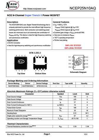
http //www.ncepower.com NCEP25N10AQ NCE N-Channel Super Trench II Power MOSFET Description General Features The NCEP25N10AQ uses Super Trench II technology that is VDS =100V,ID =27A uniquely optimized to provide the most efficient high frequency RDS(ON)=19m (typical) @ VGS=10V switching performance. Both conduction and switching power RDS(ON)=25m (typical) @ VGS=4.5V losses
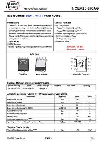
nceap25n10ad.pdf
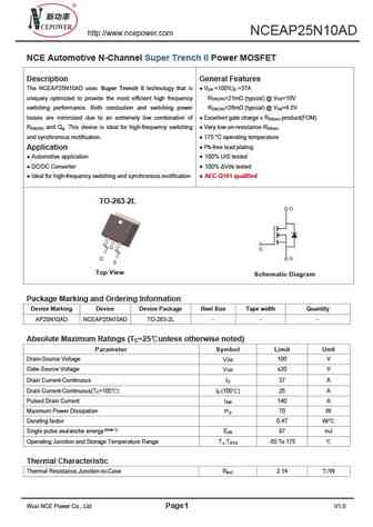
NCEAP25N10AD http //www.ncepower.com NCE Automotive N-Channel Super Trench II Power MOSFET Description General Features The NCEAP25N10AD uses Super Trench II technology that is V =100V,I =37A DS D uniquely optimized to provide the most efficient high frequency R =21m (typical) @ V =10V DS(ON) GS switching performance. Both conduction and switching power R =26m (typical) @ V =4.5
nceap25n10ag.pdf
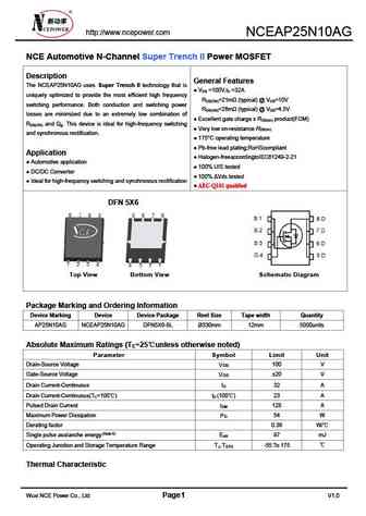
http //www.ncepower.com NCEAP25N10AG NCE Automotive N-Channel Super Trench II Power MOSFET Description General Features The NCEAP25N10AG uses Super Trench II technology that is V =100V,I =32A DS D uniquely optimized to provide the most efficient high frequency R =21m (typical) @ V =10V DS(ON) GS switching performance. Both conduction and switching power R =26m (typical) @ V
ncep25n10ag.pdf
http //www.ncepower.com NCEP25N10AG NCE N-Channel Super Trench II Power MOSFET Description General Features The NCEP25N10AG uses Super Trench II technology that is VDS =100V,ID =30A uniquely optimized to provide the most efficient high frequency RDS(ON)=21m (typical) @ VGS=10V switching performance. Both conduction and switching power RDS(ON)=26m (typical) @ VGS=4.5V losses
ncep25n10ak.pdf

http //www.ncepower.com NCEP25N10AK NCE N-Channel Super Trench II Power MOSFET Description General Features The NCEP25N10AK uses Super Trench II technology that is VDS =100V,ID =35A uniquely optimized to provide the most efficient high frequency RDS(ON)=21m (typical) @ VGS=10V switching performance. Both conduction and switching power RDS(ON)=26m (typical) @ VGS=4.5V losses
sl25n10.pdf
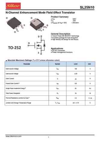
SL25N10 N-Channel Enhancement Mode Field Effect Transistor Product Summary V 100V DS I 25A D R ( at V = 10V) 45mohm DS(ON) GS General Description Trench Power MV MOSFET technology Excellent package for heat dissipation High density cell design for low R DS(ON) Applications DC-DC Converters Power management functions Absolute Maximum Rat
st25n10.pdf
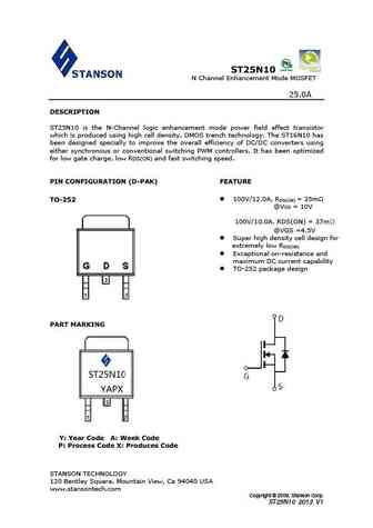
ST25N10 N Channel Enhancement Mode MOSFET 25.0A DESCRIPTION ST25N10 is the N-Channel logic enhancement mode power field effect transistor which is produced using high cell density, DMOS trench technology. The ST16N10 has been designed specially to improve the overall efficiency of DC/DC converters using either synchronous or conventional switching PWM controllers. It has been o
wmo25n10t1.pdf
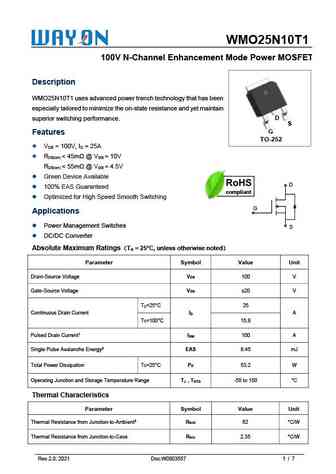
WMO25N10T1 100V N-Channel Enhancement Mode Power MOSFET Description WMO25N10T1 uses advanced power trench technology that has been especially tailored to minimize the on-state resistance and yet maintain D superior switching performance. S G Features TO-252 V = 100V, I = 25A DS D R
wmll025n10hgs.pdf
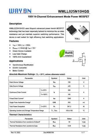
WMLL025N10HGS 100V N-Channel Enhancement Mode Power MOSFET Description D D WMLL025N10HGS uses Wayon's advanced power trench MOSFET S technology that has been especially tailored to minimize the on-state S G S S S S S S S S resistance and yet maintain superior switching performance. This S S G S S device is well suited for high efficiency fast switching applications.
wmk25n10t1.pdf
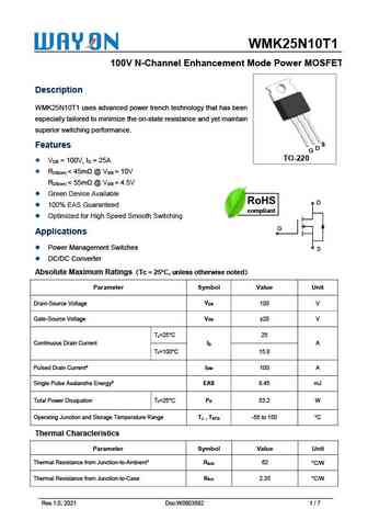
WMK25N10T1 100V N-Channel Enhancement Mode Power MOSFET Description WMK25N10T1 uses advanced power trench technology that has been especially tailored to minimize the on-state resistance and yet maintain superior switching performance. S Features D G TO-220 V = 100V, I = 25A DS D R
si25n10.pdf

N -CHANNEL ENHANCEMENT MODE POWER MOSFET SI25N10 N-Channel Enhancement Mode Power MOSFET Description TO-252 The SI25N10 uses advanced trench technology to provide D excellent RDS(ON), low gate charge and operation with gate voltages as low as 4.5V. This device is suitable for use as a S Battery protection or in other switching application. G Equivalent Circuit General Fea
aur020n10 auw025n10.pdf
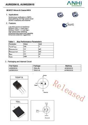
AUR020N10, AUW025N10 MOSFET Silicon N-Channel MOS 1. Applications Synchronous rectification in SMPS, Hard switching and High speed circuit DC/DC in telecoms and industrial 2. Features Low drain-source on-resistance RDS(on) TOLL = 1.6m (typ.) RDS(on) TO247 = 2.1m (typ.) High speed power switching Enhanced body diode dv/dt capability Enhanced avalanche ruggedness
agm025n10c.pdf
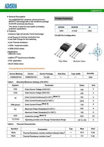
AGM025N10C Characteristics Curves Figure 2. Maximum Power Dissipation vs Case Figure 1. Safe Operating Area Temperature Figure 3. Maximum Continuous Drain Current vs Figure 4. Typical Output Characteristics Case Temperature www.agm-mos.com 3 VER2.71 AGM025N10C Figure 5. Transient Thermal Impedance Figure 7. Source-Drain Diode Forward Figure 6. Typical Transfer Characteristi
hgb025n10a.pdf
HGB025N10A P-1 100V N-Ch Power MOSFET Feature 100 V VDS High Speed Power Switching 2.0 RDS(on),typ mW Enhanced Body diode dv/dt capability 258 A ID (Sillicon Limited) Enhanced Avalanche Ruggedness 100% UIS Tested, 100% Rg Tested Lead Free, Halogen Free Application Synchronous Rectification in SMPS Hard Switching and High Speed Circuit Drain DC/D
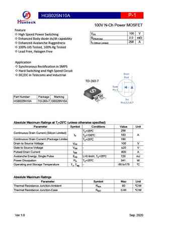
hgt025n10a.pdf
HGT025N10A P-1 100V N-Ch Power MOSFET Feature 100 V VDS High Speed Power Switching 1.97 RDS(on),typ mW Enhanced Body diode dv/dt capability 258 A ID (Sillicon Limited) Enhanced Avalanche Ruggedness 240 A ID (Package Limited) 100% UIS Tested, 100% Rg Tested Lead Free, Halogen Free Application Synchronous Rectification in SMPS Drain Hard Sw
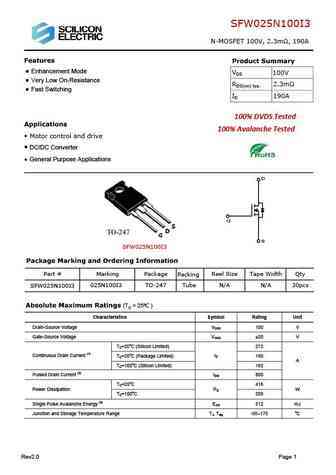
sfw025n100c3.pdf
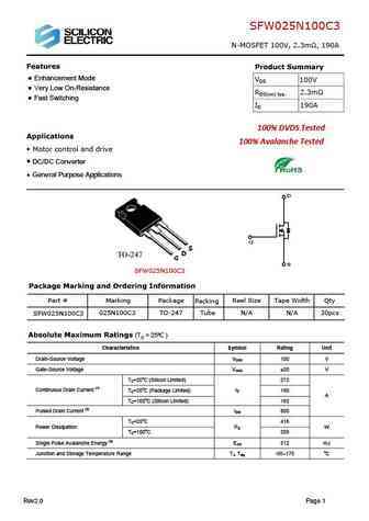
SFW025N100C3 N-MOSFET 100V, 2.3m , 190A Features Product Summary Enhancement Mode VDS 100V Very Low On-Resistance RDS(on) typ. 2.3m Fast Switching ID 190A 100% DVDS Tested Applications 100% Avalanche Tested Motor control and drive DC/DC Converter General Purpose Applications D G S SFW025N100C3 Package Marking and Ordering Information Part # M
sfw025n100i3.pdf
SFW025N100I3 N-MOSFET 100V, 2.3m , 190A Features Product Summary Enhancement Mode VDS 100V Very Low On-Resistance RDS(on) typ. 2.3m Fast Switching ID 190A 100% DVDS Tested Applications 100% Avalanche Tested Motor control and drive DC/DC Converter General Purpose Applications D G S SFW025N100I3 Package Marking and Ordering Information Part # M
sfp028n100c3 sfb025n100c3.pdf
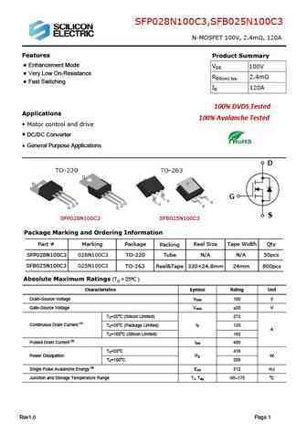
SFP028N100C3,SFB025N100C3 N-MOSFET 100V, 2.4m , 120A Features Product Summary Enhancement Mode VDS 100V Very Low On-Resistance RDS(on) typ. 2.4m Fast Switching ID 120A 100% DVDS Tested Applications 100% Avalanche Tested Motor control and drive DC/DC Converter General Purpose Applications D G S SFP028N100C3 SFB025N100C3 Package Marking and Orde
25n10.pdf
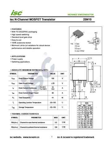
INCHANGE Semiconductor isc N-Channel MOSFET Transistor 25N10 FEATURES With TO-252(DPAK) packaging High speed switching Standard level gate drive Easy to use 100% avalanche tested Minimum Lot-to-Lot variations for robust device performance and reliable operation APPLICATIONS Power supply Switching applications ABSOLUTE MAXIMUM RATINGS(T =25 ) a SYMBOL PARAM
125n10t.pdf
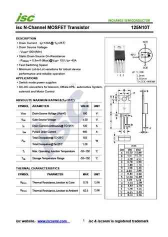
INCHANGE Semiconductor isc N-Channel MOSFET Transistor 125N10T DESCRIPTION Drain Current I =120A@ T =25 D C Drain Source Voltage- V =100V(Min) DSS Static Drain-Source On-Resistance R = 5.8m (Max)@V = 10V; I = 40A DS(on) GS D Fast Switching Speed Minimum Lot-to-Lot variations for robust device performance and reliable operation APPLICATIONS Switch mode power su
stp25n10f7.pdf
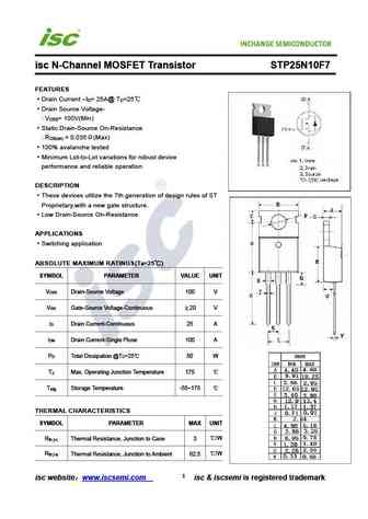
isc N-Channel MOSFET Transistor STP25N10F7 FEATURES Drain Current I = 25A@ T =25 D C Drain Source Voltage- V = 100V(Min) DSS Static Drain-Source On-Resistance R = 0.035 (Max) DS(on) 100% avalanche tested Minimum Lot-to-Lot variations for robust device performance and reliable operation DESCRIPTION These devices utilize the 7th generation of design rules of S
Другие IGBT... 24NM60G-T3B-T, 24NM60L-T3F-T, 24NM60G-T3F-T, 24NM60L-T47-T, 24NM60G-T47-T, 24NM60L-T47S-T, 25N10L-TF1-T, 25N10G-TF1-T, AO3401, 25N10G-TF2-T, 25N10L-TF3-T, 25N10G-TF3-T, 25N10L-TM3-T, 25N10G-TM3-T, 25N10L-TN3-R, 25N10G-TN3-R, 2N60L-T2Q-T
🌐 : EN ES РУ

Список транзисторов
Обновления
MOSFET: AUW033N08BG | AUW025N10 | AUR030N10 | AUR020N10 | AUR020N085 | AUR014N10 | AUP074N10 | AUP065N10 | AUP062N08BG | AUP060N08AG | HYG053N10NS1B | HYG053N10NS1P | AP220N04T | AP220N04P | QM3126M3 | AUP060N055
Popular searches
2n270 | 2n2924 | mpsa65 | 2sa794 | 2sa816 | 2sc897 datasheet | 2sd389 | mp41 transistor