HM2302KR. Аналоги и основные параметры
Наименование производителя: HM2302KR
Тип транзистора: MOSFET
Полярность: N
Предельные значения
Pd ⓘ - Максимальная рассеиваемая мощность: 1 W
|Vds|ⓘ - Максимально допустимое напряжение сток-исток: 20 V
|Vgs|ⓘ - Максимально допустимое напряжение затвор-исток: 10 V
|Id| ⓘ - Максимально допустимый постоянный ток стока: 2.9 A
Tj ⓘ - Максимальная температура канала: 150 °C
Электрические характеристики
tr ⓘ - Время нарастания: 50 ns
Cossⓘ - Выходная емкость: 120 pf
RDSonⓘ - Сопротивление сток-исток открытого транзистора: 0.045 Ohm
Тип корпуса: SOT323
Аналог (замена) для HM2302KR
- подборⓘ MOSFET транзистора по параметрам
HM2302KR даташит
hm2302kr.pdf
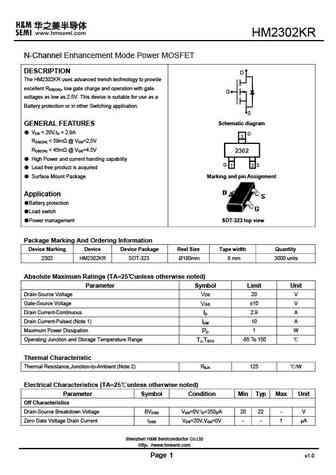
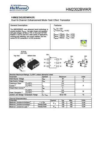
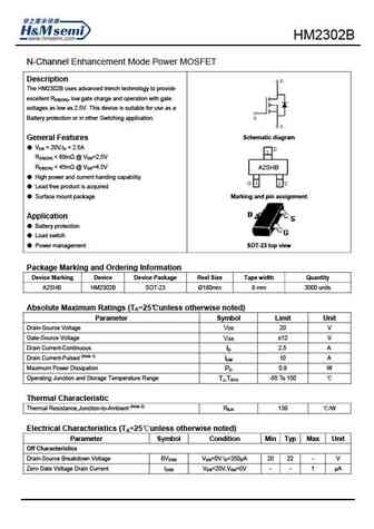
HM2302KR N-Channel Enhancement Mode Power MOSFET DESCRIPTION D The HM2302KR uses advanced trench technology to provide excellent RDS(ON), low gate charge and operation with gate G voltages as low as 2.5V. This device is suitable for use as a Battery protection or in other Switching application. S Schematic diagram GENERAL FEATURES VDS = 20V,ID = 2.9A D 3 RDS(ON)
hm2302.pdf

HM2302 N-Channel Enhancement Mode Power MOSFET DESCRIPTION D The HM2302 uses advanced trench technology to provide excellent RDS(ON), low gate charge and operation with gate G voltages as low as 2.5V. This device is suitable for use as a Battery protection or in other Switching application. S Schematic diagram GENERAL FEATURES VDS = 20V,ID = 2.9A D 3 RDS(ON)
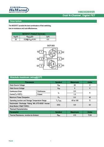
hm2302bwsr.pdf
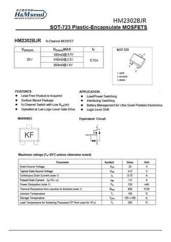
Description The MOSFET provide the best combination of fast switching, low on-resistance and cost-effectiveness. MOSFET Product Summary VDS(V) RDS(on)( ) ID(A) 20 0.29@ VGS=4.5V 0.5 SOT-563 S2 1 D2 6 G2 2 G1 5 4 S1 3 D1 Absolute maximum rating@25 Parameter Symbol Maximum Units Drain-Source Voltage
hm2302f.pdf

HM2302F N-Channel Enhancement Mode Power MOSFET Description The HM2302F uses advanced trench technology to provide excellent RDS(ON), low gate charge and operation with gate voltages as low as 2.5V. This device is suitable for use as a Battery protection or in other Switching application. Schematic diagram General Features VDS = 20V,ID = 2.8A RDS(ON)


Другие MOSFET... HM2302B , HM2302BJR , HM2302BWKR , HM2302BWSR , HM2302D , HM2302DR , HM2302E , HM2302F , 20N60 , HM2305 , HM2305B , HM2305D , HM2306 , HM2309 , HM2309AL , HM2309APR , HM2309B .
🌐 : EN ES РУ

Список транзисторов
Обновления
MOSFET: AUN084N10 | AUN065N10 | AUN063N10 | AUN062N08BG | AUN060N08AG | AUN053N10 | AUN050N08BGL | AUN045N085 | AUN042N055 | AUN036N10 | AUD069N10A | AUD062N08BG | AUD060N08AG | AUD060N055 | AUD056N08BGL | AUB062N08BG
Popular searches
c1815 transistor | 2sc1815 | irfz44 | 2n5551 | irf540n | irf3205 mosfet | 2n3055 | irfp260n