HM25P15K - Аналоги. Основные параметры
Наименование производителя: HM25P15K
Тип транзистора: MOSFET
Полярность: P
Pd ⓘ - Максимальная рассеиваемая мощность: 160 W
|Vds|ⓘ - Предельно допустимое напряжение сток-исток: 150 V
|Vgs|ⓘ - Предельно допустимое напряжение затвор-исток: 20 V
|Id| ⓘ - Максимально допустимый постоянный ток стока: 25 A
Tj ⓘ - Максимальная температура канала: 150 °C
tr ⓘ - Время нарастания: 80 ns
Cossⓘ - Выходная емкость: 148 pf
Rds ⓘ - Сопротивление сток-исток открытого транзистора: 0.135 Ohm
Тип корпуса: TO-252
Аналог (замена) для HM25P15K
HM25P15K технические параметры
hm25p15k.pdf
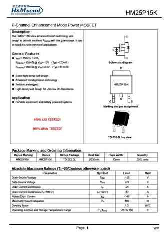
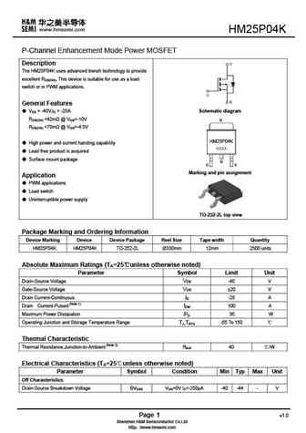
HM25P15K P-Channel Enhancement Mode Power MOSFET Description The HM25P15K uses advanced trench technology and design to provide excellent RDS(ON) with low gate charge. It can be used in a wide variety of applications. General Features VDS =-150V,ID =-25A RDS(ON)
hm25p15d.pdf
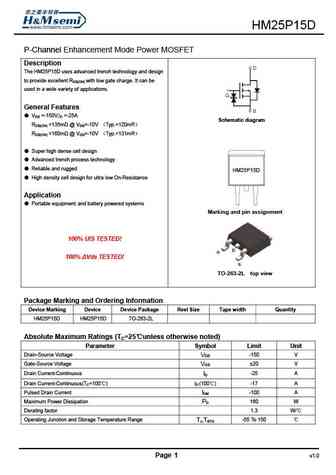
HM25P15D P-Channel Enhancement Mode Power MOSFET Description The HM25P15D uses advanced trench technology and design to provide excellent RDS(ON) with low gate charge. It can be used in a wide variety of applications. General Features VDS =-150V,ID =-25A Schematic diagram RDS(ON)
hm25p15.pdf
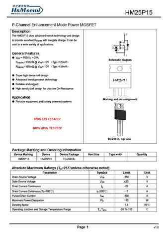
HM25P15 P-Channel Enhancement Mode Power MOSFET Description The HM25P15 uses advanced trench technology and design to provide excellent RDS(ON) with low gate charge. It can be used in a wide variety of applications. General Features VDS =-150V,ID =-25A Schematic diagram RDS(ON)
hm25p06d.pdf

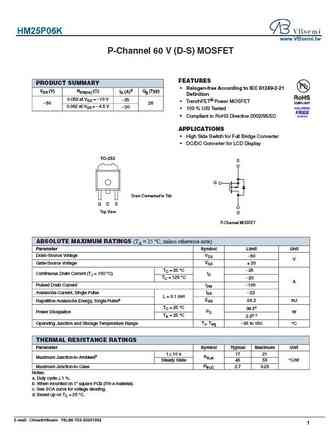
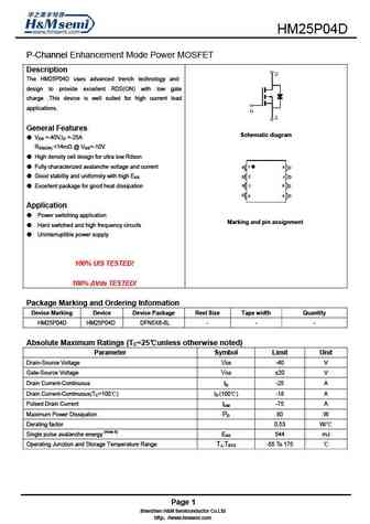
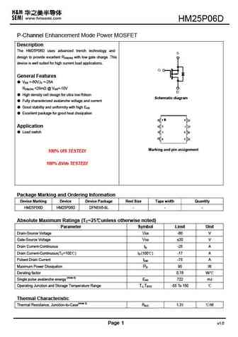
HM25P06D P-Channel Enhancement Mode Power MOSFET Description The HM25P06D uses advanced trench technology and design to provide excellent RDS(ON) with low gate charge .This device is well suited for high current load applications. General Features VDS =-60V,ID =-25A RDS(ON)
Другие MOSFET... HM25N50 , HM25P03D , HM25P03K , HM25P03Q , HM25P04D , HM25P04K , HM25P15 , HM25P15D , AON6380 , HM26N18K , HM2800D , HM2803D , HM2807 , HM2807D , HM2809D , HM2809DR , HM2907 .


Список транзисторов
Обновления
MOSFET: AP6007S | AP5N50K | AP5N20K | AP5N10S | AP5N10M | AP50P20Q | AP50P20K | AP50P06K | AP50N06K | AP50N04QD | AP50N04Q | AP50N04K | AP50N04GD | AP5040QD | AP4946S | AP4847
Popular searches
irf640n datasheet | irf540 datasheet | irf530 | 2n3565 | irf530n | pn2222a datasheet | tip41c transistor | 2n5087