HM3426B. Аналоги и основные параметры
Наименование производителя: HM3426B
Тип транзистора: MOSFET
Полярность: N
Предельные значения
Pd ⓘ - Максимальная рассеиваемая мощность: 3.5 W
|Vds|ⓘ - Максимально допустимое напряжение сток-исток: 30 V
|Vgs|ⓘ - Максимально допустимое напряжение затвор-исток: 20 V
|Id| ⓘ - Максимально допустимый постоянный ток стока: 18 A
Tj ⓘ - Максимальная температура канала: 150 °C
Электрические характеристики
tr ⓘ - Время нарастания: 10 ns
Cossⓘ - Выходная емкость: 318 pf
RDSonⓘ - Сопротивление сток-исток открытого транзистора: 0.01 Ohm
Тип корпуса: SOT89
Аналог (замена) для HM3426B
- подборⓘ MOSFET транзистора по параметрам
HM3426B даташит
hm3426b.pdf
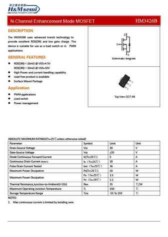
N-Channel Enhancement Mode MOSFET HM3426B DESCRIPTION The HM3426B uses advanced trench technology to provide excellent RDS(ON) and low gate charge. This device is suitable for use as a load switch or in PWM applications. GENERAL FEATURES RDS(ON)
hm3422.pdf
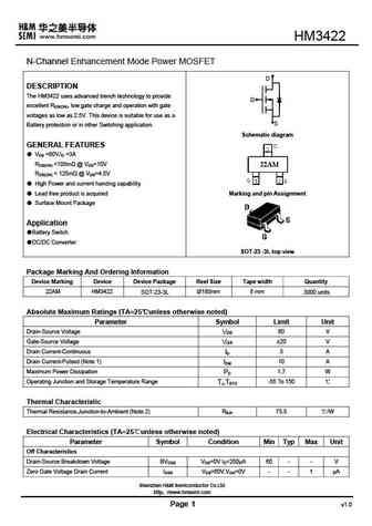
HM3422 N-Channel Enhancement Mode Power MOSFET D DESCRIPTION The HM3422 uses advanced trench technology to provide G excellent RDS(ON), low gate charge and operation with gate voltages as low as 2.5V. This device is suitable for use as a S Battery protection or in other Switching application. Schematic diagram GENERAL FEATURES VDS =60V,ID =3A RDS(ON)
hm3421b.pdf

HM3421B P-Channel Enhancement Mode Power MOSFET DESCRIPTION D The HM3421B uses advanced trench technology to provide excellent RDS(ON), low gate charge and operation with gate G voltages as low as 2.5V. This device is suitable for use as a load switch or in PWM applications. S Schematic diagram GENERAL FEATURES VDS = -30V,ID = -4.2A RDS(ON)
hm3422a.pdf
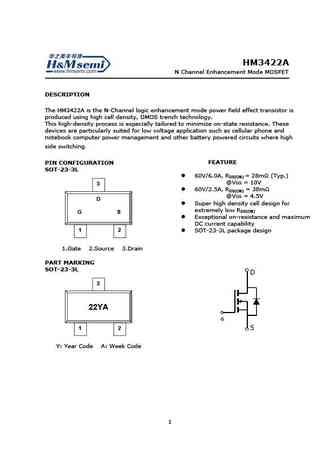
HM N Channel Enhancement Mode MOSFET DESCRIPTION The HM3422A is the N-Channel logic enhancement mode power field effect transistor is produced using high cell density, DMOS trench technology. This high-density process is especially tailored to minimize on-state resistance. These devices are particularly suited for low voltage application such as cellular phone and notebook co

Другие IGBT... HM3414, HM3414B, HM3415E, HM3416B, HM3421, HM3421B, HM3422, HM3422A, STP75NF75, HM35N03D, HM35N03Q, HM35P03, HM35P03D, HM35P03K, HM35P04D, HM3710, HM3710K
History: CEDM8001
🌐 : EN ES РУ

Список транзисторов
Обновления
MOSFET: AKF30N5P0SX | AKF30N10S | AKF20P45D | CM4407 | CM3407 | CM3400 | SVF11N65F | SVF11N65T | FKBB3105 | EHBA036R1 | CRTT067N10N | AP6NA3R2MT | AP65SA145DDT8 | AP4NAR95CMT-A | AP4024GEMT-HF | AP3P050AH
Popular searches
mpsa56 | c3205 transistor | tip35c datasheet | 2n5401 datasheet | mj21194g | irfz34n | mn2488 | irfb438