HM4611. Аналоги и основные параметры
Наименование производителя: HM4611
Тип транзистора: MOSFET
Полярность: NP
Предельные значения
Pd ⓘ
- Максимальная рассеиваемая мощность: 2 W
|Vds|ⓘ - Максимально допустимое напряжение сток-исток: 60 V
|Vgs|ⓘ - Максимально допустимое напряжение затвор-исток: 20 V
|Id| ⓘ - Максимально допустимый постоянный ток стока: 4.5 A
Tj ⓘ - Максимальная температура канала: 150 °C
Электрические характеристики
tr ⓘ -
Время нарастания: 2.3 ns
Cossⓘ - Выходная емкость: 60 pf
RDSonⓘ - Сопротивление сток-исток открытого транзистора: 0.045 Ohm
Тип корпуса: SOP8
Аналог (замена) для HM4611
- подборⓘ MOSFET транзистора по параметрам
HM4611 даташит
..1. Size:949K cn hmsemi
hm4611.pdf 

N and P-Channel Enhancement Mode Power MOSFET Description The uses advanced trench technology to provide excellent RDS(ON) and low gate charge . General Features N-Channel N-channel P-channel VDS = V,ID = Schematic diagram RDS(ON)
0.1. Size:1105K cn hmsemi
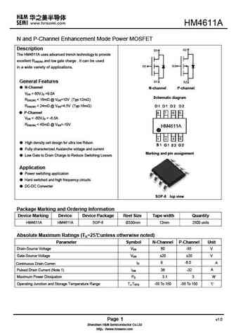
hm4611a.pdf 

HM4611A N and P-Channel Enhancement Mode Power MOSFET Description The HM4611A uses advanced trench technology to provide excellent RDS(ON) and low gate charge . It can be used in a wide variety of applications. General Features N-Channel N-channel P-channel VDS = 60V,ID =9.0A Schematic diagram RDS(ON)
0.2. Size:709K cn hmsemi
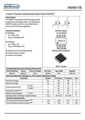
hm4611b.pdf 

HM4611B N and P-Channel Enhancement Mode Power MOSFET Description The HM4611B uses advanced trench technology to provide excellent RDS(ON) and low gate charge . The complementary MOSFETs may be used to form a level shifted high side switch, and for a host of other applications. Schematic diagram General Features N-Channel VDS = 60V,ID =6.3A RDS(ON)
9.1. Size:830K cn hmsemi
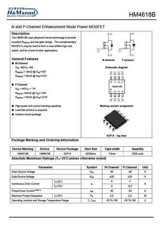
hm4618b.pdf 

HM4618B N and P-Channel Enhancement Mode Power MOSFET Description The HM4618B uses advanced trench technology to provide excellent RDS(ON) and low gate charge . The complementary MOSFETs may be used to form a level shifted high side switch, and for a host of other applications. General Features N-channel P-channel N-Channel VDS =40V,ID =8A Schematic diagram RDS(ON)
9.2. Size:753K cn hmsemi
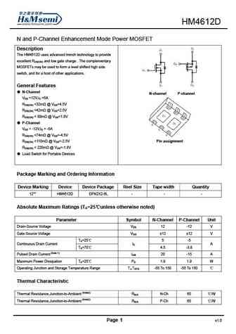
hm4612d.pdf 

HM4612D N and P-Channel Enhancement Mode Power MOSFET Description The HM4612D uses advanced trench technology to provide excellent RDS(ON) and low gate charge . The complementary MOSFETs may be used to form a level shifted high side switch, and for a host of other applications. General Features N-Channel N-channel P-channel VDS =12V,ID =5A RDS(ON)
9.3. Size:715K cn hmsemi
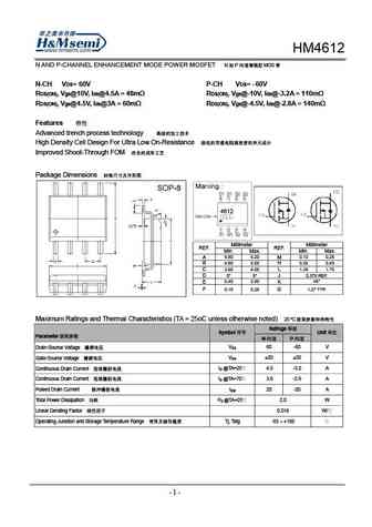
hm4612.pdf 

HM N AND P-CHANNEL ENHANCEMENT MODE POWER MOSFET N P MOS N-CH VDS= 60V P-CH VDS= - 60V RDS(ON), Vgs@10V, Ids@4.5A = 48m RDS(ON), Vgs@-10V, Ids@-3.2A = 110m RDS(ON), Vgs@4.5V, Ids@3A = 60m RDS(ON), Vgs@-4.5V, Ids@-2.8A = 140m Features Advanced trench process technology High Density Cell Design For Ultra Low On-Resistan
9.5. Size:1361K cn hmsemi
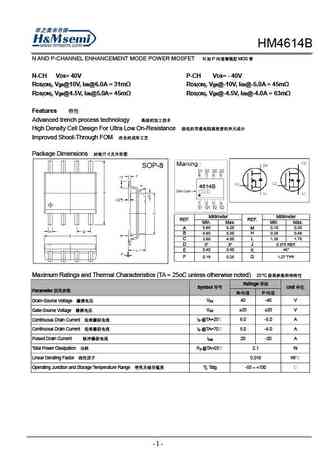
hm4614b.pdf 

HM N AND P-CHANNEL ENHANCEMENT MODE POWER MOSFET N P MOS N-CH VDS= 40V P-CH VDS= - 40V RDS(ON), Vgs@10V, Ids@6.0A = 31m RDS(ON), Vgs@-10V, Ids@-5.0A = 45m RDS(ON), Vgs@4.5V, Ids@5.0A= 45m RDS(ON), Vgs@-4.5V, Ids@-4.0A = 63m Features Advanced trench process technology High Density Cell Design For Ultra Low On-Resist
9.6. Size:980K cn hmsemi
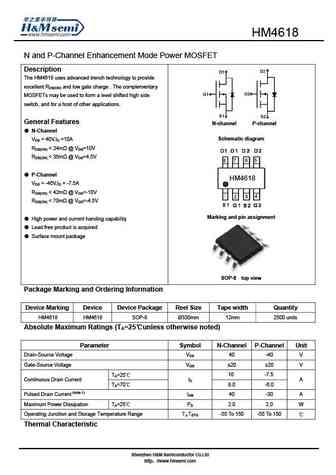
hm4618.pdf 

HM4618 N and P-Channel Enhancement Mode Power MOSFET Description The HM4618 uses advanced trench technology to provide excellent RDS(ON) and low gate charge . The complementary MOSFETs may be used to form a level shifted high side switch, and for a host of other applications. General Features N-channel P-channel N-Channel Schematic diagram VDS = 40V,ID =10A RDS(ON)
9.7. Size:659K cn hmsemi
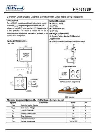
hm4618sp.pdf 

HM4618SP Common-Drain Dual N-Channel Enhancement Mode Field Effect Transistor Description General Features The HM4618SP uses advanced trench technology to provide VSSS =20V,IS =6A excellent RSS(ON), low gate charge and operation with gate 2.5V drive voltages as low as 2.5V while retaining a 12V VGS(MAX) rating. It Common-drain type is ESD protected. This device is
9.8. Size:874K cn hmsemi
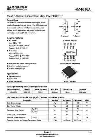
hm4616a.pdf 

N and P-Channel Enhancement Mode Power MOSFET Description The uses advanced trench technology to provide excellent RDS(ON) and low gate charge . The SOP-8 package is universally preferred for all commercial industrial surface mount applications and suited for low voltage applications such as DC/DC converters. N-channel P-channel General Features N-Channel
9.9. Size:922K cn hmsemi
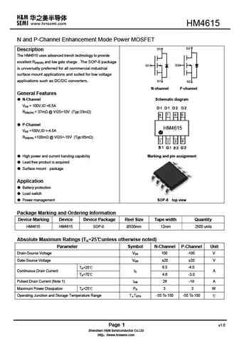
hm4615.pdf 

HM4615 N and P-Channel Enhancement Mode Power MOSFET Description The HM4615 uses advanced trench technology to provide excellent RDS(ON) and low gate charge . The SOP-8 package is universally preferred for all commercial industrial surface mount applications and suited for low voltage applications such as DC/DC converters. N-channel P-channel General Features N-Channel Sc
9.10. Size:579K cn hmsemi
hm4616.pdf 

N and P-Channel Enhancement Mode Power MOSFET Description The uses advanced trench technology to provide excellent RDS(ON) and low gate charge . The SOP-8 package is universally preferred for all commercial industrial surface mount applications and suited for low voltage applications such as DC/DC converters. N-channel P-channel General Features N-Channel
Другие MOSFET... HM45P02D
, HM45P02Q
, HM45P03K
, HM4606
, HM4606A
, HM4606B
, HM4606C
, HM4606D
, TK10A60D
, HM4611A
, HM4611B
, HM4612
, HM4612D
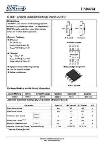
, HM4614
, HM4614B
, HM4615
, HM4616
.
History: BSO072N03S
| PSMN4R3-100ES
| PSMN4R3-100PS
| FQA32N20C

