NTMFS1D15N03CGT1G. Аналоги и основные параметры
Наименование производителя: NTMFS1D15N03CGT1G
Тип транзистора: MOSFET
Полярность: N
Предельные значения
Pd ⓘ - Максимальная рассеиваемая мощность: 124 W
|Vds|ⓘ - Максимально допустимое напряжение сток-исток: 30 V
|Vgs|ⓘ - Максимально допустимое напряжение затвор-исток: 20 V
|Id| ⓘ - Максимально допустимый постоянный ток стока: 245 A
Tj ⓘ - Максимальная температура канала: 175 °C
Электрические характеристики
tr ⓘ - Время нарастания: 13 ns
Cossⓘ - Выходная емкость: 3600 pf
RDSonⓘ - Сопротивление сток-исток открытого транзистора: 0.00115 Ohm
Тип корпуса: DFN5
Аналог (замена) для NTMFS1D15N03CGT1G
- подборⓘ MOSFET транзистора по параметрам
NTMFS1D15N03CGT1G даташит
ntmfs1d15n03cg.pdf
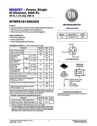
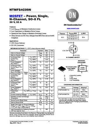
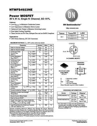
MOSFET - Power, Single N-Channel, SO8-FL 30 V, 1.15 mW, 245 A NTMFS1D15N03CG Features Advanced Package (5x6 mm) with Excellent Thermal Conduction www.onsemi.com Ultra Low RDS(on) to Improve System Efficiency These Devices are Pb-Free and are RoHS Compliant V(BR)DSS RDS(ON) MAX ID MAX Typical Applications 30 V 1.15 mW @ 10 V 245 A Hot Swap Application Power Load
ntmfs1d15n03cgt1g.pdf

MOSFET - Power, Single N-Channel, SO8-FL 30 V, 1.15 mW, 245 A NTMFS1D15N03CG Features Advanced Package (5x6 mm) with Excellent Thermal Conduction www.onsemi.com Ultra Low RDS(on) to Improve System Efficiency These Devices are Pb-Free and are RoHS Compliant V(BR)DSS RDS(ON) MAX ID MAX Typical Applications 30 V 1.15 mW @ 10 V 245 A Hot Swap Application Power Load
ntmfs1d7n03cgt1g.pdf
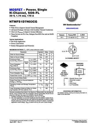
MOSFET - Power, Single N-Channel, SO8-FL 30 V, 1.74 mW, 170 A NTMFS1D7N03CG Features Wide SOA to Improve Inrush Current Management www.onsemi.com Advanced Package (5x6 mm) with Excellent Thermal Conduction Ultra Low RDS(on) to Improve System Efficiency These Devices are Pb-Free, Halogen Free/BFR Free and are RoHS V(BR)DSS RDS(ON) MAX ID MAX Compliant 30 V 1.74 mW @ 1
ntmfs5c442nlt1g.pdf
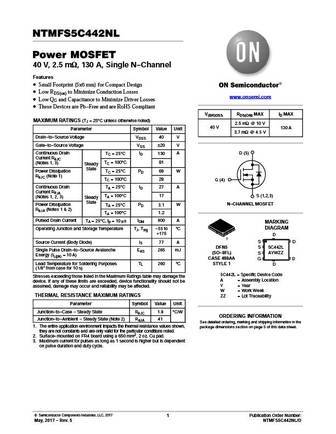
NTMFS5C442NL Power MOSFET 40 V, 2.5 mW, 130 A, Single N-Channel Features Small Footprint (5x6 mm) for Compact Design Low RDS(on) to Minimize Conduction Losses www.onsemi.com Low QG and Capacitance to Minimize Driver Losses These Devices are Pb-Free and are RoHS Compliant V(BR)DSS RDS(ON) MAX ID MAX MAXIMUM RATINGS (TJ = 25 C unless otherwise noted) 2.5 mW @ 10 V 40
ntmfs5c628nlt1g.pdf

NTMFS5C628NL Power MOSFET 60 V, 2.4 mW, 150 A, Single N-Channel Features Small Footprint (5x6 mm) for Compact Design Low RDS(on) to Minimize Conduction Losses www.onsemi.com Low QG and Capacitance to Minimize Driver Losses These Devices are Pb-Free and are RoHS Compliant V(BR)DSS RDS(ON) MAX ID MAX MAXIMUM RATINGS (TJ = 25 C unless otherwise noted) 2.4 mW @ 10 V 60
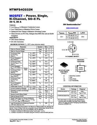
ntmfs4c55n.pdf
NTMFS4C55N Power MOSFET 30 V, 78 A, Single N-Channel, SO-8 FL Features Low RDS(on) to Minimize Conduction Losses Low Capacitance to Minimize Driver Losses Optimized Gate Charge to Minimize Switching Losses www.onsemi.com These Devices are Pb-Free, Halogen Free/BFR Free and are RoHS Compliant V(BR)DSS RDS(ON) MAX ID MAX Applications 3.4 mW @ 10 V CPU Power Delive
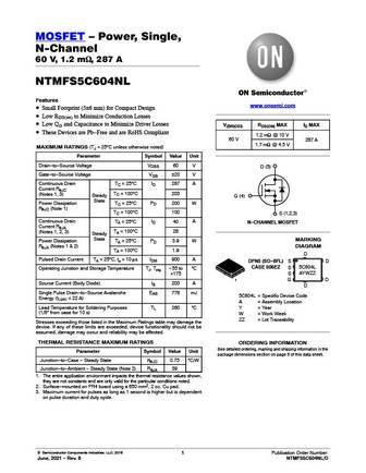
ntmfs5c604nlt1g.pdf

NTMFS5C604NL Power MOSFET 60 V, 1.2 mW, 287 A, Single N-Channel Features Small Footprint (5x6 mm) for Compact Design Low RDS(on) to Minimize Conduction Losses www.onsemi.com Low QG and Capacitance to Minimize Driver Losses These Devices are Pb-Free and are RoHS Compliant V(BR)DSS RDS(ON) MAX ID MAX MAXIMUM RATINGS (TJ = 25 C unless otherwise noted) 1.2 mW @ 10 V 60
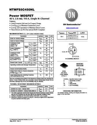
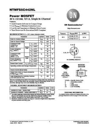
ntmfs5c450nlt3g.pdf
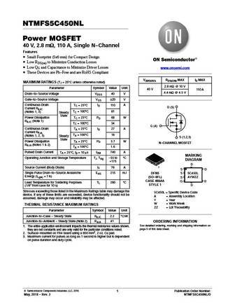
NTMFS5C450NL Power MOSFET 40 V, 2.8 mW, 110 A, Single N-Channel Features Small Footprint (5x6 mm) for Compact Design Low RDS(on) to Minimize Conduction Losses Low QG and Capacitance to Minimize Driver Losses www.onsemi.com These Devices are Pb-Free and are RoHS Compliant V(BR)DSS RDS(ON) MAX ID MAX MAXIMUM RATINGS (TJ = 25 C unless otherwise noted) 2.8 mW @ 10 V Par
ntmfs5c406nlt1g.pdf
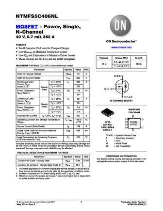
NTMFS5C406NL MOSFET Power, Single, N-Channel 40 V, 0.7 mW, 362 A Features www.onsemi.com Small Footprint (5x6 mm) for Compact Design Low RDS(on) to Minimize Conduction Losses Low QG and Capacitance to Minimize Driver Losses V(BR)DSS RDS(ON) MAX ID MAX These Devices are Pb-Free and are RoHS Compliant 0.7 mW @ 10 V 40 V 362 A MAXIMUM RATINGS (TJ = 25 C unless oth
ntmfs5c612nt1g-te.pdf
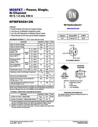
MOSFET Power, Single, N-Channel 60 V, 1.6 mW, 230 A NTMFS5C612N Features www.onsemi.com Small Footprint (5x6 mm) for Compact Design Low RDS(on) to Minimize Conduction Losses Low QG and Capacitance to Minimize Driver Losses These Devices are Pb-Free and are RoHS Compliant V(BR)DSS RDS(ON) MAX ID MAX 60 V 1.6 mW @ 10 V 230 A MAXIMUM RATINGS (TJ = 25 C unless otherw
ntmfs5c450nt3g.pdf
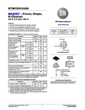
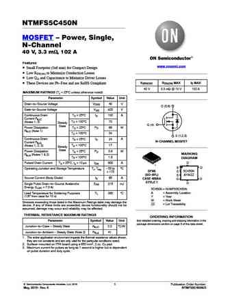
NTMFS5C450N MOSFET Power, Single, N-Channel 40 V, 3.3 mW, 102 A Features www.onsemi.com Small Footprint (5x6 mm) for Compact Design Low RDS(on) to Minimize Conduction Losses Low QG and Capacitance to Minimize Driver Losses V(BR)DSS RDS(ON) MAX ID MAX These Devices are Pb-Free and are RoHS Compliant 40 V 3.3 mW @ 10 V 102 A MAXIMUM RATINGS (TJ = 25 C unless other
ntmfs5c426nt1g.pdf

MOSFET Power, Single N-Channel 40 V, 1.3 mW, 235 A NTMFS5C426N Features www.onsemi.com Small Footprint (5x6 mm) for Compact Design Low RDS(on) to Minimize Conduction Losses Low QG and Capacitance to Minimize Driver Losses V(BR)DSS RDS(ON) MAX ID MAX These Devices are Pb-Free and are RoHS Compliant 40 V 1.3 mW @ 10 V 235 A MAXIMUM RATINGS (TJ = 25 C unless otherw
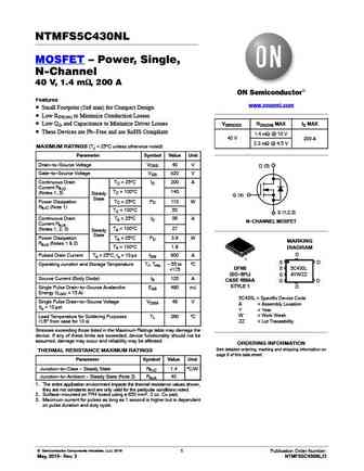
ntmfs5c430nlt1g.pdf
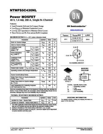
NTMFS5C430NL Power MOSFET 40 V, 1.4 mW, 200 A, Single N-Channel Features Small Footprint (5x6 mm) for Compact Design Low RDS(on) to Minimize Conduction Losses www.onsemi.com Low QG and Capacitance to Minimize Driver Losses These Devices are Pb-Free and are RoHS Compliant V(BR)DSS RDS(ON) MAX ID MAX MAXIMUM RATINGS (TJ = 25 C unless otherwise noted) 1.4 mW @ 10 V 40
ntmfs5c426nlt1g.pdf

ON Semiconductor Is Now To learn more about onsemi , please visit our website at www.onsemi.com onsemi and and other names, marks, and brands are registered and/or common law trademarks of Semiconductor Components Industries, LLC dba onsemi or its affiliates and/or subsidiaries in the United States and/or other countries. onsemi owns the rights to a number of patents, trademarks,
ntmfs5c646nlt3g.pdf

NTMFS5C646NL Power MOSFET 60 V, 4.7 mW, 93 A, Single N-Channel Features Small Footprint (5x6 mm) for Compact Design Low RDS(on) to Minimize Conduction Losses www.onsemi.com Low QG and Capacitance to Minimize Driver Losses These Devices are Pb-Free, Halogen Free/BFR Free and are RoHS Compliant V(BR)DSS RDS(ON) MAX ID MAX 4.7 mW @ 10 V MAXIMUM RATINGS (TJ = 25 C unles
ntmfs3d6n10mclt1g.pdf
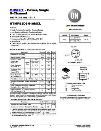
MOSFET - Power, Single N-Channel 100 V, 3.6 mW, 131 A NTMFS3D6N10MCL Features www.onsemi.com Small Footprint (5x6 mm) for Compact Design Low RDS(on) to Minimize Conduction Losses Low QG and Capacitance to Minimize Driver Losses V(BR)DSS RDS(ON) MAX ID MAX Primary DC-DC MOSFET 3.6 mW @ 10 V Synchronous Rectifier in DC-DC and AC-DC 100 V 131 A 5.8 mW @ 4.5 V
ntmfs5c456nlt3g.pdf
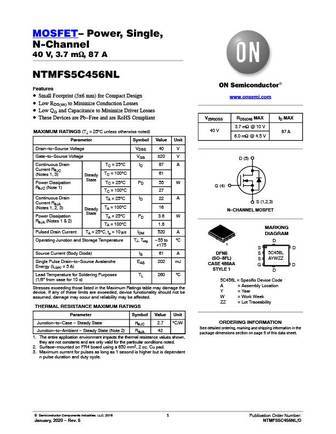
MOSFET Power, Single, N-Channel 40 V, 3.7 mW, 87 A NTMFS5C456NL Features Small Footprint (5x6 mm) for Compact Design www.onsemi.com Low RDS(on) to Minimize Conduction Losses Low QG and Capacitance to Minimize Driver Losses V(BR)DSS RDS(ON) MAX ID MAX These Devices are Pb-Free and are RoHS Compliant 3.7 mW @ 10 V 40 V 87 A MAXIMUM RATINGS (TJ = 25 C unless other
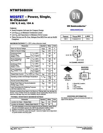
ntmfs6b05nt1g.pdf
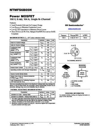
NTMFS6B05N Power MOSFET 100 V, 8 mW, 104 A, Single N-Channel Features Small Footprint (5x6 mm) for Compact Design Low RDS(on) to Minimize Conduction Losses www.onsemi.com Low QG and Capacitance to Minimize Driver Losses These Devices are Pb-Free, Halogen Free/BFR Free and are RoHS Compliant V(BR)DSS RDS(ON) MAX ID MAX MAXIMUM RATINGS (TJ = 25 C unless otherwise noted
ntmfs0d8n02p1et1g.pdf

MOSFET - Power, Single N-Channel, SO8-FL 25 V, 0.68 mW, 365 A NTMFS0D8N02P1E Features Small Footprint (5x6mm) for Compact Design www.onsemi.com Low RDS(on) to Minimize Conduction Losses Low QG and Capacitance to Minimize Driver Losses These Devices are Pb-Free, Halogen Free/BFR Free and are RoHS V(BR)DSS RDS(ON) MAX ID MAX Compliant 0.68 mW @ 10 V 25 V 365 A Applic
ntmfs23d9n06hlt1g.pdf
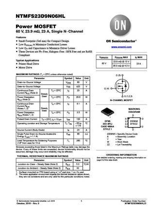
NTMFS23D9N06HL Power MOSFET 60 V, 23.9 mW, 23 A, Single N-Channel Features Small Footprint (5x6 mm) for Compact Design Low RDS(on) to Minimize Conduction Losses www.onsemi.com Low QG and Capacitance to Minimize Driver Losses These Devices are Pb-Free, Halogen-Free / BFR Free and are RoHS Compliant V(BR)DSS RDS(ON) MAX ID MAX Typical Applications 23.9 mW @ 10 V 60 V
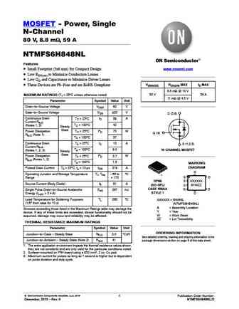
ntmfs6h848nlt1g.pdf
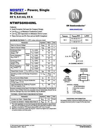
MOSFET - Power, Single N-Channel 80 V, 8.8 mW, 59 A NTMFS6H848NL Features www.onsemi.com Small Footprint (5x6 mm) for Compact Design Low RDS(on) to Minimize Conduction Losses Low QG and Capacitance to Minimize Driver Losses V(BR)DSS RDS(ON) MAX ID MAX These Devices are Pb-Free and are RoHS Compliant 8.8 mW @ 10 V MAXIMUM RATINGS (TJ = 25 C unless otherwise noted) 80
ntmfs0d9n03cgt1g.pdf

MOSFET - Power, Single N-Channel, SO8-FL 30 V, 0.9 mW, 298 A NTMFS0D9N03CG Features www.onsemi.com Advanced Package (5x6mm) with Excellent Thermal Conduction Ultra Low RDS(on) to Improve System Efficiency These Devices are Pb-Free, Halogen Free/BFR Free and are RoHS V(BR)DSS RDS(ON) MAX ID MAX Compliant 30 V 0.9 mW @ 10 V 298 A Applications Hot Swap Application D (
ntmfs5c406nt1g.pdf
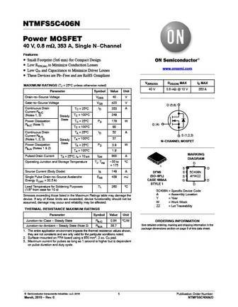
NTMFS5C406N Power MOSFET 40 V, 0.8 mW, 353 A, Single N-Channel Features Small Footprint (5x6 mm) for Compact Design Low RDS(on) to Minimize Conduction Losses www.onsemi.com Low QG and Capacitance to Minimize Driver Losses These Devices are Pb-Free and are RoHS Compliant V(BR)DSS RDS(ON) MAX ID MAX MAXIMUM RATINGS (TJ = 25 C unless otherwise noted) 40 V 0.8 mW @ 10 V
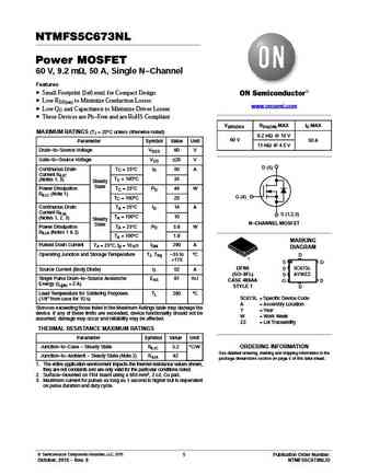
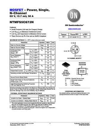
ntmfs5c673nt1g.pdf
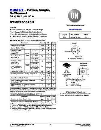
MOSFET Power, Single, N-Channel 60 V, 10.7 mW, 50 A NTMFS5C673N Features www.onsemi.com Small Footprint (5x6 mm) for Compact Design Low RDS(on) to Minimize Conduction Losses Low QG and Capacitance to Minimize Driver Losses V(BR)DSS RDS(ON) MAX ID MAX These Devices are Pb-Free and are RoHS Compliant 60 V 10.7 mW @ 10 V 50 A MAXIMUM RATINGS (TJ = 25 C unless other
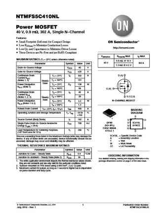
ntmfs5c410nt3g.pdf
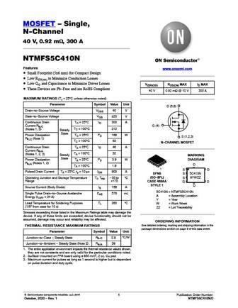
MOSFET Single, N-Channel 40 V, 0.92 mW, 300 A NTMFS5C410N Features www.onsemi.com Small Footprint (5x6 mm) for Compact Design Low RDS(on) to Minimize Conduction Losses Low QG and Capacitance to Minimize Driver Losses V(BR)DSS RDS(ON) MAX ID MAX These Devices are Pb-Free and are RoHS Compliant 40 V 0.92 mW @ 10 V 300 A MAXIMUM RATINGS (TJ = 25 C unless otherwise
ntmfs5c645nlt3g.pdf

NTMFS5C645NL Power MOSFET 60 V, 4.0 mW, 100 A, Single N-Channel Features Small Footprint (5x6 mm) for Compact Design Low RDS(on) to Minimize Conduction Losses www.onsemi.com Low QG and Capacitance to Minimize Driver Losses These Devices are Pb-Free and are RoHS Compliant V(BR)DSS RDS(ON) MAX ID MAX MAXIMUM RATINGS (TJ = 25 C unless otherwise noted) 4.0 mW @ 10 V 60
ntmfs5c646nlt1g.pdf
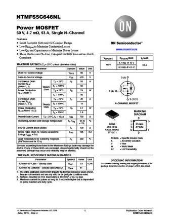
NTMFS5C646NL Power MOSFET 60 V, 4.7 mW, 93 A, Single N-Channel Features Small Footprint (5x6 mm) for Compact Design Low RDS(on) to Minimize Conduction Losses www.onsemi.com Low QG and Capacitance to Minimize Driver Losses These Devices are Pb-Free, Halogen Free/BFR Free and are RoHS Compliant V(BR)DSS RDS(ON) MAX ID MAX 4.7 mW @ 10 V MAXIMUM RATINGS (TJ = 25 C unles
ntmfs5c423nlt1g.pdf
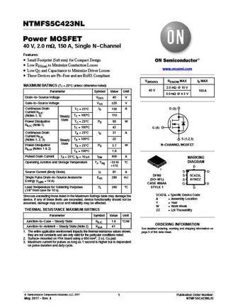
NTMFS5C423NL Power MOSFET 40 V, 2.0 mW, 150 A, Single N-Channel Features Small Footprint (5x6 mm) for Compact Design Low RDS(on) to Minimize Conduction Losses www.onsemi.com Low QG and Capacitance to Minimize Driver Losses These Devices are Pb-Free and are RoHS Compliant V(BR)DSS RDS(ON) MAX ID MAX MAXIMUM RATINGS (TJ = 25 C unless otherwise noted) 2.0 mW @ 10 V 40
ntmfs5c404nt3g.pdf
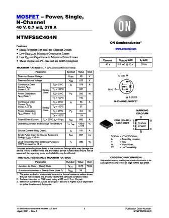
MOSFET Power, Single, N-Channel 40 V, 0.7 mW, 378 A NTMFS5C404N Features www.onsemi.com Small Footprint (5x6 mm) for Compact Design Low RDS(on) to Minimize Conduction Losses Low QG and Capacitance to Minimize Driver Losses V(BR)DSS RDS(ON) MAX ID MAX These Devices are Pb-Free and are RoHS Compliant 40 V 0.7 mW @ 10 V 378 A MAXIMUM RATINGS (TJ = 25 C unless other
ntmfs5c670nlt3g.pdf

NTMFS5C670NL Power MOSFET 60 V, 6.1 mW, 71 A, Single N-Channel Features Small Footprint (5x6 mm) for Compact Design Low RDS(on) to Minimize Conduction Losses www.onsemi.com Low QG and Capacitance to Minimize Driver Losses These Devices are Pb-Free and are RoHS Compliant V(BR)DSS RDS(ON) MAX ID MAX MAXIMUM RATINGS (TJ = 25 C unless otherwise noted) 6.1 mW @ 10 V 60 V
ntmfs6b05nt3g.pdf
NTMFS6B05N MOSFET Power, Single, N-Channel 100 V, 8 mW, 104 A Features www.onsemi.com Small Footprint (5x6 mm) for Compact Design Low RDS(on) to Minimize Conduction Losses Low QG and Capacitance to Minimize Driver Losses V(BR)DSS RDS(ON) MAX ID MAX These Devices are Pb-Free, Halogen Free/BFR Free and are RoHS 100 V 8 mW @ 10 V 104 A Compliant MAXIMUM RATINGS (TJ
ntmfs5h425nlt1g.pdf
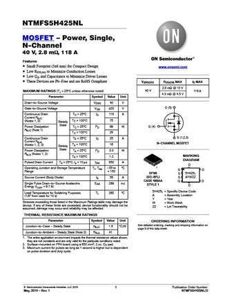
NTMFS5H425NL MOSFET Power, Single, N-Channel 40 V, 2.8 mW, 118 A Features Small Footprint (5x6 mm) for Compact Design www.onsemi.com Low RDS(on) to Minimize Conduction Losses Low QG and Capacitance to Minimize Driver Losses These Devices are Pb-Free and are RoHS Compliant V(BR)DSS RDS(ON) MAX ID MAX 2.8 mW @ 10 V 40 V MAXIMUM RATINGS (TJ = 25 C unless otherwise
ntmfs5c612nlt1g.pdf
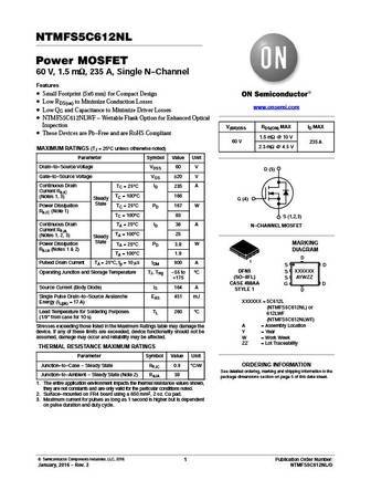
NTMFS5C612NL Power MOSFET 60 V, 1.5 mW, 235 A, Single N-Channel Features Small Footprint (5x6 mm) for Compact Design Low RDS(on) to Minimize Conduction Losses www.onsemi.com Low QG and Capacitance to Minimize Driver Losses NTMFS5C612NLWF - Wettable Flank Option for Enhanced Optical Inspection V(BR)DSS RDS(ON) MAX ID MAX These Devices are Pb-Free and are RoHS Compl
ntmfs4d2n10mdt1g.pdf

ON Semiconductor Is Now To learn more about onsemi , please visit our website at www.onsemi.com onsemi and and other names, marks, and brands are registered and/or common law trademarks of Semiconductor Components Industries, LLC dba onsemi or its affiliates and/or subsidiaries in the United States and/or other countries. onsemi owns the rights to a number of patents, trademarks,
ntmfs006n12mct1g.pdf
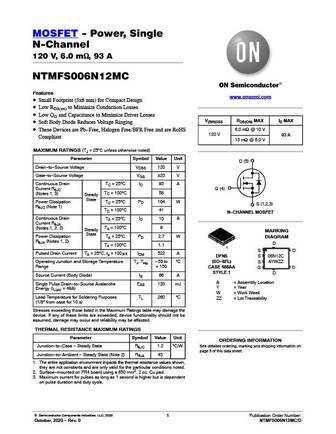
MOSFET - Power, Single N-Channel 120 V, 6.0 mW, 93 A NTMFS006N12MC Features www.onsemi.com Small Footprint (5x6 mm) for Compact Design Low RDS(on) to Minimize Conduction Losses Low QG and Capacitance to Minimize Driver Losses V(BR)DSS RDS(ON) MAX ID MAX Soft Body Diode Reduces Voltage Ringing 6.0 mW @ 10 V These Devices are Pb-Free, Halogen Free/BFR Free and are
ntmfs6h818nlt1g.pdf
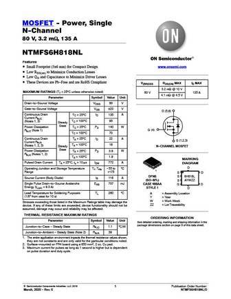
MOSFET - Power, Single N-Channel 80 V, 3.2 mW, 135 A NTMFS6H818NL Features www.onsemi.com Small Footprint (5x6 mm) for Compact Design Low RDS(on) to Minimize Conduction Losses Low QG and Capacitance to Minimize Driver Losses These Devices are Pb-Free and are RoHS Compliant V(BR)DSS RDS(ON) MAX ID MAX 3.2 mW @ 10 V MAXIMUM RATINGS (TJ = 25 C unless otherwise noted)
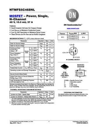
ntmfs5c468nlt1g.pdf
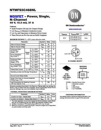
NTMFS5C468NL MOSFET Power, Single, N-Channel 40 V, 10.3 mW, 37 A Features Small Footprint (5x6 mm) for Compact Design www.onsemi.com Low RDS(on) to Minimize Conduction Losses Low QG and Capacitance to Minimize Driver Losses V(BR)DSS RDS(ON) MAX ID MAX These Devices are Pb-Free and are RoHS Compliant 10.3 mW @ 10 V 40 V 37 A MAXIMUM RATINGS (TJ = 25 C unless ot
ntmfs5c604nlt3g.pdf
MOSFET Power, Single, N-Channel 60 V, 1.2 mW, 287 A NTMFS5C604NL Features www.onsemi.com Small Footprint (5x6 mm) for Compact Design Low RDS(on) to Minimize Conduction Losses Low QG and Capacitance to Minimize Driver Losses V(BR)DSS RDS(ON) MAX ID MAX These Devices are Pb-Free and are RoHS Compliant 1.2 mW @ 10 V 60 V 287 A 1.7 mW @ 4.5 V MAXIMUM RATINGS (TJ =
ntmfs5c609nlt1g.pdf
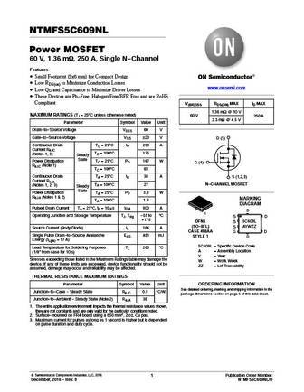
NTMFS5C609NL Power MOSFET 60 V, 1.36 mW, 250 A, Single N-Channel Features Small Footprint (5x6 mm) for Compact Design Low RDS(on) to Minimize Conduction Losses www.onsemi.com Low QG and Capacitance to Minimize Driver Losses These Devices are Pb-Free, Halogen Free/BFR Free and are RoHS Compliant V(BR)DSS RDS(ON) MAX ID MAX 1.36 mW @ 10 V MAXIMUM RATINGS (TJ = 25 C un
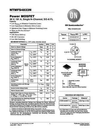
ntmfs5844nlt1g.pdf
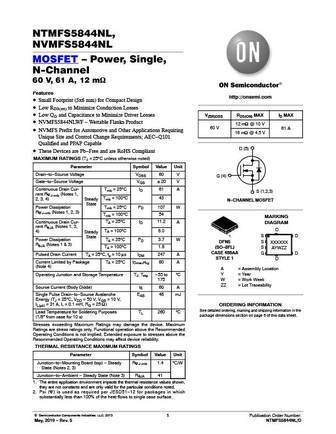
NTMFS5844NL, NVMFS5844NL MOSFET Power, Single, N-Channel 60 V, 61 A, 12 mW Features http //onsemi.com Small Footprint (5x6 mm) for Compact Design Low RDS(on) to Minimize Conduction Losses Low QG and Capacitance to Minimize Driver Losses V(BR)DSS RDS(ON) MAX ID MAX NVMFS5844NLWF - Wettable Flanks Product 12 mW @ 10 V 60 V 61 A NVMFS Prefix for Automotive and
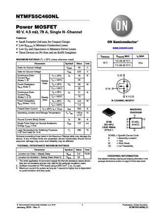
ntmfs5c460nlt3g.pdf
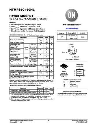
NTMFS5C460NL Power MOSFET 40 V, 4.5 mW, 78 A, Single N-Channel Features Small Footprint (5x6 mm) for Compact Design Low RDS(on) to Minimize Conduction Losses www.onsemi.com Low QG and Capacitance to Minimize Driver Losses These Devices are Pb-Free and are RoHS Compliant V(BR)DSS RDS(ON) MAX ID MAX MAXIMUM RATINGS (TJ = 25 C unless otherwise noted) 4.5 mW @ 10 V 40 V
ntmfs6b14nt3g.pdf

NTMFS6B14N MOSFET Power, Single, N-Channel 100 V, 15 mW, 50 A Features www.onsemi.com Small Footprint (5x6 mm) for Compact Design Low RDS(on) to Minimize Conduction Losses Low QG and Capacitance to Minimize Driver Losses V(BR)DSS RDS(ON) MAX ID MAX These Devices are Pb-Free, Halogen Free/BFR Free and are RoHS 100 V 15 mW @ 10 V 50 A Compliant MAXIMUM RATINGS (TJ
ntmfs008n12mct1g.pdf

ON Semiconductor Is Now To learn more about onsemi , please visit our website at www.onsemi.com onsemi and and other names, marks, and brands are registered and/or common law trademarks of Semiconductor Components Industries, LLC dba onsemi or its affiliates and/or subsidiaries in the United States and/or other countries. onsemi owns the rights to a number of patents, trademarks,
ntmfs4c06n.pdf
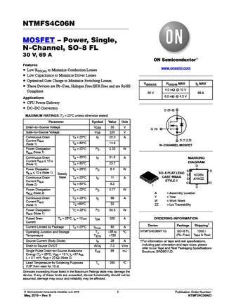
NTMFS4C06N MOSFET Power, Single, N-Channel, SO-8 FL 30 V, 69 A Features www.onsemi.com Low RDS(on) to Minimize Conduction Losses Low Capacitance to Minimize Driver Losses Optimized Gate Charge to Minimize Switching Losses V(BR)DSS RDS(ON) MAX ID MAX These Devices are Pb-Free, Halogen Free/BFR Free and are RoHS 4.0 mW @ 10 V Compliant 30 V 69 A 6.0 mW @ 4.5 V A
ntmfs5c673nlt1g.pdf
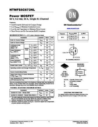
NTMFS5C673NL Power MOSFET 60 V, 9.2 mW, 50 A, Single N-Channel Features Small Footprint (5x6 mm) for Compact Design Low RDS(on) to Minimize Conduction Losses www.onsemi.com Low QG and Capacitance to Minimize Driver Losses These Devices are Pb-Free and are RoHS Compliant V(BR)DSS RDS(ON) MAX ID MAX MAXIMUM RATINGS (TJ = 25 C unless otherwise noted) 9.2 mW @ 10 V 60 V
ntmfs6h852nlt1g.pdf

MOSFET - Power, Single N-Channel 80 V, 13.1 mW, 42 A NTMFS6H852NL Features www.onsemi.com Small Footprint (5x6 mm) for Compact Design Low RDS(on) to Minimize Conduction Losses Low QG and Capacitance to Minimize Driver Losses V(BR)DSS RDS(ON) MAX ID MAX These Devices are Pb-Free and are RoHS Compliant 13.1 mW @ 10 V MAXIMUM RATINGS (TJ = 25 C unless otherwise noted)
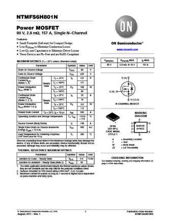
ntmfs6h801nt1g.pdf
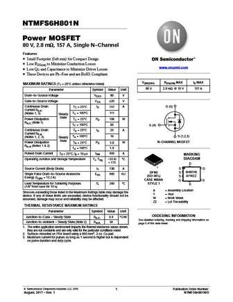
NTMFS6H801N Power MOSFET 80 V, 2.8 mW, 157 A, Single N-Channel Features Small Footprint (5x6 mm) for Compact Design Low RDS(on) to Minimize Conduction Losses www.onsemi.com Low QG and Capacitance to Minimize Driver Losses These Devices are Pb-Free and are RoHS Compliant V(BR)DSS RDS(ON) MAX ID MAX MAXIMUM RATINGS (TJ = 25 C unless otherwise noted) 80 V 2.8 mW @ 10 V
ntmfs5c645nlt1g.pdf
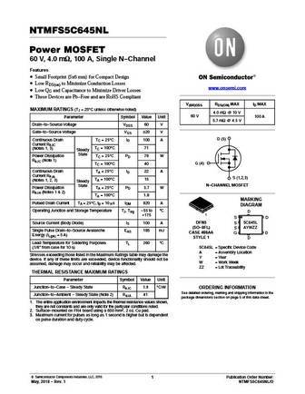
NTMFS5C645NL Power MOSFET 60 V, 4.0 mW, 100 A, Single N-Channel Features Small Footprint (5x6 mm) for Compact Design Low RDS(on) to Minimize Conduction Losses www.onsemi.com Low QG and Capacitance to Minimize Driver Losses These Devices are Pb-Free and are RoHS Compliant V(BR)DSS RDS(ON) MAX ID MAX MAXIMUM RATINGS (TJ = 25 C unless otherwise noted) 4.0 mW @ 10 V 60
ntmfs4c05nt1g.pdf
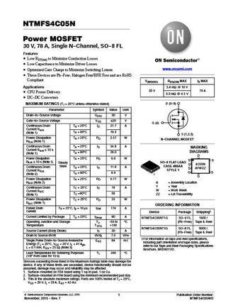
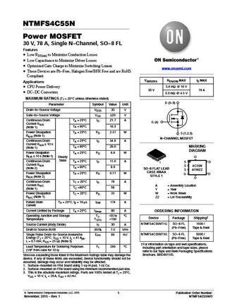
NTMFS4C05N Power MOSFET 30 V, 78 A, Single N-Channel, SO-8 FL Features Low RDS(on) to Minimize Conduction Losses Low Capacitance to Minimize Driver Losses www.onsemi.com Optimized Gate Charge to Minimize Switching Losses These Devices are Pb-Free, Halogen Free/BFR Free and are RoHS Compliant V(BR)DSS RDS(ON) MAX ID MAX Applications 3.4 mW @ 10 V 30 V 78 A CPU P
ntmfs5c628nt1g.pdf
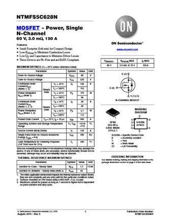
NTMFS5C628N MOSFET - Power, Single N-Channel 60 V, 3.0 mW, 150 A Features Small Footprint (5x6 mm) for Compact Design www.onsemi.com Low RDS(on) to Minimize Conduction Losses Low QG and Capacitance to Minimize Driver Losses These Devices are Pb-Free and are RoHS Compliant V(BR)DSS RDS(ON) MAX ID MAX 60 V 3.0 mW @ 10 V 150 A MAXIMUM RATINGS (TJ = 25 C unless otherwis

ntmfs5c442nt3g.pdf
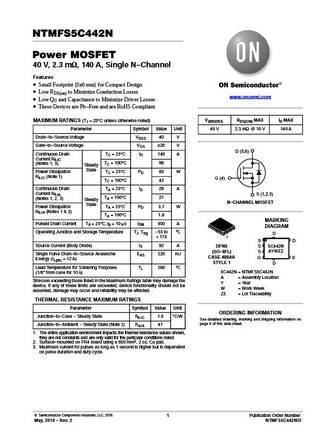
NTMFS5C442N Power MOSFET 40 V, 2.3 mW, 140 A, Single N-Channel Features Small Footprint (5x6 mm) for Compact Design Low RDS(on) to Minimize Conduction Losses www.onsemi.com Low QG and Capacitance to Minimize Driver Losses These Devices are Pb-Free and are RoHS Compliant V(BR)DSS RDS(ON) MAX ID MAX MAXIMUM RATINGS (TJ = 25 C unless otherwise noted) Parameter Symbol Va
ntmfs5c430nlt3g.pdf
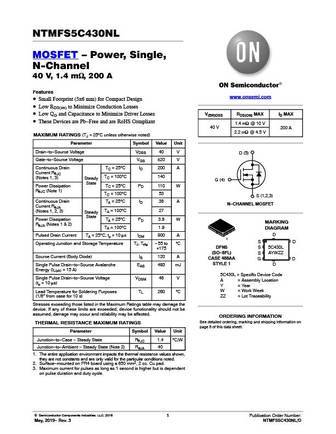
NTMFS5C430NL MOSFET Power, Single, N-Channel 40 V, 1.4 mW, 200 A Features www.onsemi.com Small Footprint (5x6 mm) for Compact Design Low RDS(on) to Minimize Conduction Losses Low QG and Capacitance to Minimize Driver Losses V(BR)DSS RDS(ON) MAX ID MAX These Devices are Pb-Free and are RoHS Compliant 1.4 mW @ 10 V 40 V 200 A 2.2 mW @ 4.5 V MAXIMUM RATINGS (TJ =
ntmfs5c404nltt1g.pdf
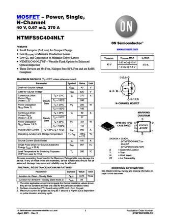
MOSFET Power, Single, N-Channel 40 V, 0.67 mW, 370 A NTMFS5C404NLT Features www.onsemi.com Small Footprint (5x6 mm) for Compact Design Low RDS(on) to Minimize Conduction Losses Low QG and Capacitance to Minimize Driver Losses V(BR)DSS RDS(ON) MAX ID MAX NTMFS5C404NLTWF - Wettable Flank Option for Enhanced 0.67 mW @ 10 V 40 V 370 A Optical Inspection 1.0 mW @ 4.
ntmfs5c670nt1g.pdf
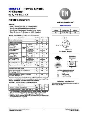
MOSFET Power, Single, N-Channel 60 V, 7.0 mW, 71 A NTMFS5C670N Features www.onsemi.com Small Footprint (5x6 mm) for Compact Design Low RDS(on) to Minimize Conduction Losses Low QG and Capacitance to Minimize Driver Losses V(BR)DSS RDS(ON) MAX ID MAX These Devices are Pb-Free and are RoHS Compliant 60 V 7.0 mW @ 10 V 71 A MAXIMUM RATINGS (TJ = 25 C unless otherwis
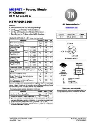
ntmfs6h836nlt1g.pdf
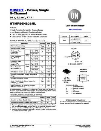
MOSFET - Power, Single N-Channel 80 V, 6.2 mW, 77 A NTMFS6H836NL Features www.onsemi.com Small Footprint (5x6 mm) for Compact Design Low RDS(on) to Minimize Conduction Losses Low QG and Capacitance to Minimize Driver Losses V(BR)DSS RDS(ON) MAX ID MAX These Devices are Pb-Free and are RoHS Compliant 6.2 mW @ 10 V 80 V MAXIMUM RATINGS (TJ = 25 C unless otherwise not
ntmfs4943nt1g.pdf
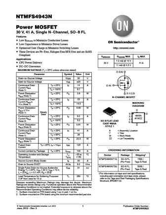
NTMFS4943N Power MOSFET 30 V, 41 A, Single N-Channel, SO-8 FL Features Low RDS(on) to Minimize Conduction Losses Low Capacitance to Minimize Driver Losses Optimized Gate Charge to Minimize Switching Losses http //onsemi.com These Devices are Pb-Free, Halogen Free/BFR Free and are RoHS Compliant V(BR)DSS RDS(ON) MAX ID MAX Applications 7.2 mW @ 10 V CPU Power Deli
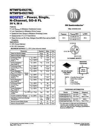
ntmfs4847nat1g ntmfs4847nt1g.pdf

NTMFS4847N Power MOSFET 30 V, 85 A, Single N-Channel, SO-8FL Features Low RDS(on) to Minimize Conduction Losses Low Capacitance to Minimize Driver Losses Optimized Gate Charge to Minimize Switching Losses http //onsemi.com Thermally Enhanced SO-8 Package These are Pb-Free Devices V(BR)DSS RDS(ON) MAX ID MAX Applications 4.1 mW @ 10 V Refer to Application Not
ntmfs4826ne.pdf
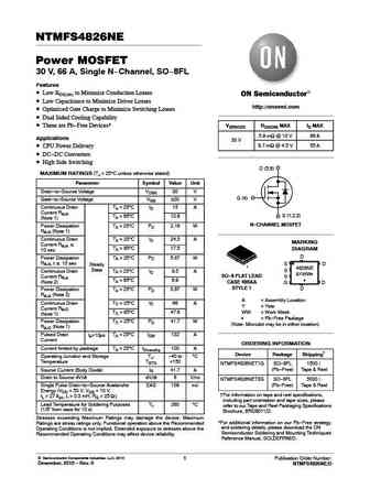
NTMFS4826NE Power MOSFET 30 V, 66 A, Single N-Channel, SO-8FL Features Low RDS(on) to Minimize Conduction Losses Low Capacitance to Minimize Driver Losses http //onsemi.com Optimized Gate Charge to Minimize Switching Losses Dual Sided Cooling Capability These are Pb-Free Devices* V(BR)DSS RDS(ON) MAX ID MAX 5.9 mW @ 10 V 66 A Applications 30 V 8.7 mW @ 4.5 V 55
ntmfs4849nt1g.pdf

NTMFS4849N Power MOSFET 30 V, 71 A, Single N-Channel, SO-8FL Features Low RDS(on) to Minimize Conduction Losses Low Capacitance to Minimize Driver Losses Optimized Gate Charge to Minimize Switching Losses http //onsemi.com Thermally Enhanced SO8 Package These are Pb-Free Devices V(BR)DSS RDS(ON) MAX ID MAX Applications 5.1 mW @ 10 V Refer to Application Note
ntmfs5c430n.pdf
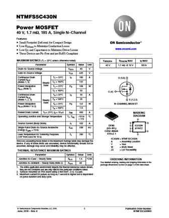
NTMFS5C430N Power MOSFET 40 V, 1.7 mW, 185 A, Single N-Channel Features Small Footprint (5x6 mm) for Compact Design Low RDS(on) to Minimize Conduction Losses www.onsemi.com Low QG and Capacitance to Minimize Driver Losses These Devices are Pb-Free and are RoHS Compliant MAXIMUM RATINGS (TJ = 25 C unless otherwise noted) V(BR)DSS RDS(ON) MAX ID MAX Parameter Symbol Va
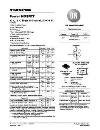
ntmfs4707nt1g.pdf
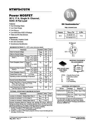
NTMFS4707N Power MOSFET 30 V, 17 A, Single N-Channel, SOIC-8 Flat Lead Features Fast Switching Times http //onsemi.com Low Gate Charge Low RDS(on) V(BR)DSS RDS(on) Typ ID Max Low Inductance SOIC-8 Package These are Pb-Free Devices 10 mW @ 10 V 30 V 17 A 13.5 mW @ 4.5 V Applications Notebooks, Graphics Cards DC-DC Converters N-Channel Synchronou
ntmfs4c054n.pdf
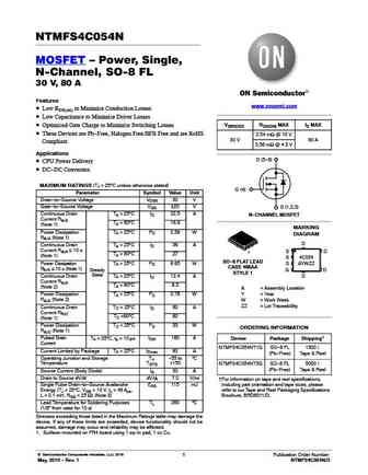
NTMFS4C054N MOSFET Power, Single, N-Channel, SO-8 FL 30 V, 80 A Features www.onsemi.com Low RDS(on) to Minimize Conduction Losses Low Capacitance to Minimize Driver Losses V(BR)DSS RDS(ON) MAX ID MAX Optimized Gate Charge to Minimize Switching Losses These Devices are Pb-Free, Halogen Free/BFR Free and are RoHS 2.54 mW @ 10 V 30 V 80 A Compliant 3.56 mW @ 4.5 V
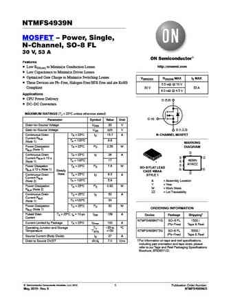
ntmfs4744n-d.pdf
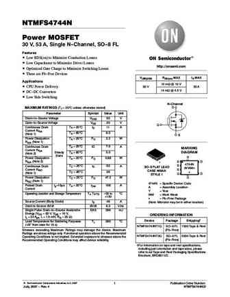
NTMFS4744N Power MOSFET 30 V, 53 A, Single N-Channel, SO-8 FL Features Low RDS(on) to Minimize Conduction Losses Low Capacitance to Minimize Driver Losses http //onsemi.com Optimized Gate Charge to Minimize Switching Losses These are Pb-Free Devices V(BR)DSS RDS(on) MAX ID MAX Applications 10 mW @ 10 V CPU Power Delivery 30 V 53 A 14 mW @ 4.5 V DC-DC Conver
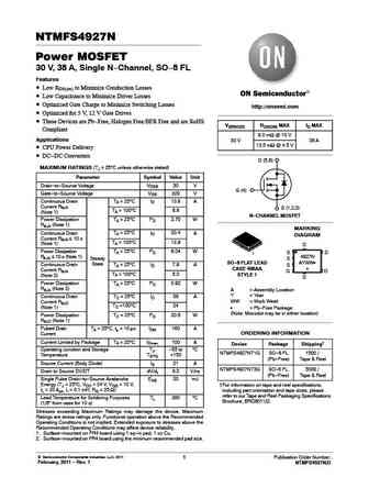
ntmfs4927nct1g ntmfs4927nt1g.pdf
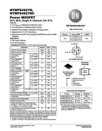
NTMFS4927N, NTMFS4927NC Power MOSFET 30 V, 38 A, Single N-Channel, SO-8 FL Features Low RDS(on) to Minimize Conduction Losses Low Capacitance to Minimize Driver Losses http //onsemi.com Optimized Gate Charge to Minimize Switching Losses Optimized for 5 V, 12 V Gate Drives These Devices are Pb-Free, Halogen Free/BFR Free and are RoHS V(BR)DSS RDS(ON) MAX ID MAX Com
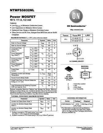
ntmfs4825nfe.pdf
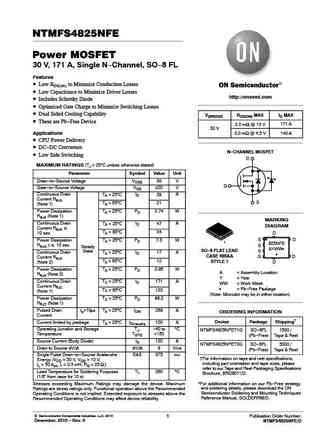
NTMFS4825NFE Power MOSFET 30 V, 171 A, Single N-Channel, SO-8 FL Features Low RDS(on) to Minimize Conduction Losses Low Capacitance to Minimize Driver Losses http //onsemi.com Includes Schottky Diode Optimized Gate Charge to Minimize Switching Losses Dual Sided Cooling Capability V(BR)DSS RDS(ON) MAX ID MAX These are Pb-Free Device 2.0 mW @ 10 V 171 A 30 V
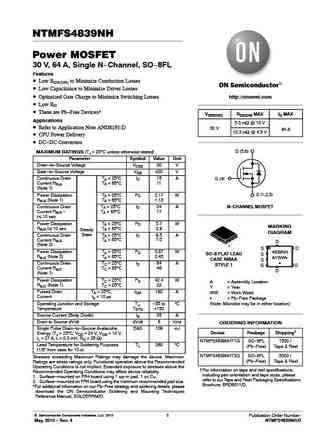
ntmfs4839n.pdf
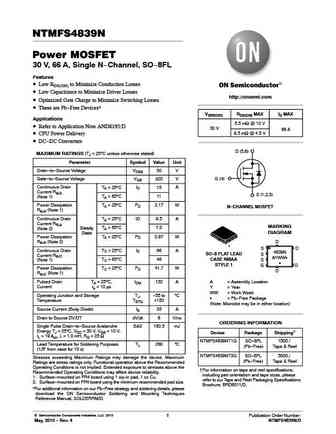
NTMFS4839N Power MOSFET 30 V, 66 A, Single N-Channel, SO-8FL Features Low RDS(ON) to Minimize Conduction Losses Low Capacitance to Minimize Driver Losses http //onsemi.com Optimized Gate Charge to Minimize Switching Losses These are Pb-Free Devices* V(BR)DSS RDS(ON) MAX ID MAX Applications 5.5 mW @ 10 V Refer to Application Note AND8195/D 30 V 66 A 9.5 mW @ 4.
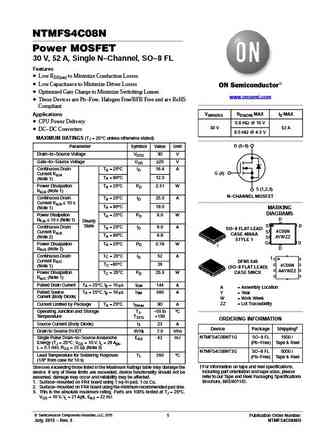
ntmfs4c55n.pdf
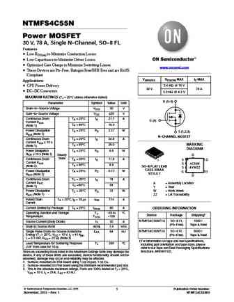
NTMFS4C55N Power MOSFET 30 V, 78 A, Single N-Channel, SO-8 FL Features Low RDS(on) to Minimize Conduction Losses Low Capacitance to Minimize Driver Losses Optimized Gate Charge to Minimize Switching Losses www.onsemi.com These Devices are Pb-Free, Halogen Free/BFR Free and are RoHS Compliant V(BR)DSS RDS(ON) MAX ID MAX Applications 3.4 mW @ 10 V CPU Power Delive
ntmfs4927-d.pdf
NTMFS4927N Power MOSFET 30 V, 38 A, Single N-Channel, SO-8 FL Features Low RDS(on) to Minimize Conduction Losses Low Capacitance to Minimize Driver Losses Optimized Gate Charge to Minimize Switching Losses http //onsemi.com Optimized for 5 V, 12 V Gate Drives These Devices are Pb-Free, Halogen Free/BFR Free and are RoHS V(BR)DSS RDS(ON) MAX ID MAX Compliant 9.0 m
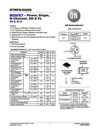
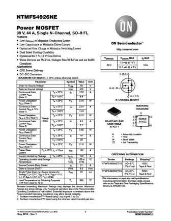
ntmfs4926nt1g.pdf

NTMFS4926N Power MOSFET 30 V, 44 A, Single N-Channel, SO-8 FL Features Low RDS(on) to Minimize Conduction Losses Low Capacitance to Minimize Driver Losses Optimized Gate Charge to Minimize Switching Losses http //onsemi.com Optimized for 5 V, 12 V Gate Drives These Devices are Pb-Free, Halogen Free/BFR Free and are RoHS V(BR)DSS RDS(ON) MAX ID MAX Compliant 7.0 m
ntmfs6h801n.pdf
NTMFS6H801N Power MOSFET 80 V, 2.8 mW, 157 A, Single N-Channel Features Small Footprint (5x6 mm) for Compact Design Low RDS(on) to Minimize Conduction Losses www.onsemi.com Low QG and Capacitance to Minimize Driver Losses These Devices are Pb-Free and are RoHS Compliant V(BR)DSS RDS(ON) MAX ID MAX MAXIMUM RATINGS (TJ = 25 C unless otherwise noted) 80 V 2.8 mW @ 10 V
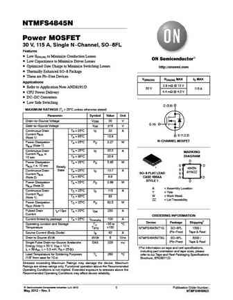
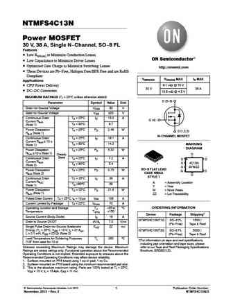
ntmfs5h425nl.pdf
NTMFS5H425NL MOSFET Power, Single, N-Channel 40 V, 2.8 mW, 118 A Features Small Footprint (5x6 mm) for Compact Design www.onsemi.com Low RDS(on) to Minimize Conduction Losses Low QG and Capacitance to Minimize Driver Losses These Devices are Pb-Free and are RoHS Compliant V(BR)DSS RDS(ON) MAX ID MAX 2.8 mW @ 10 V 40 V MAXIMUM RATINGS (TJ = 25 C unless otherwise
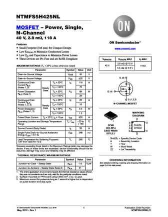
ntmfs4845nt1g.pdf
NTMFS4845N Power MOSFET 30 V, 115 A, Single N-Channel, SO-8FL Features Low RDS(on) to Minimize Conduction Losses Low Capacitance to Minimize Driver Losses Optimized Gate Charge to Minimize Switching Losses http //onsemi.com Thermally Enhanced SO-8 Package These are Pb-Free Devices V(BR)DSS RDS(ON) MAX ID MAX Applications 2.9 mW @ 10 V Refer to Application No
ntmfs4c022n.pdf
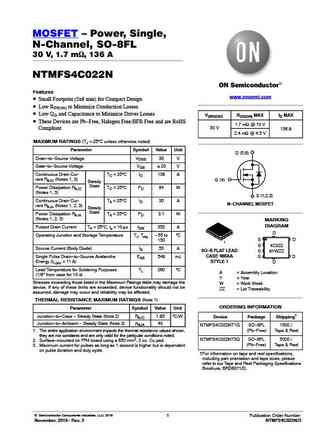
MOSFET Power, Single, N-Channel, SO-8FL 30 V, 1.7 mW, 136 A NTMFS4C022N Features www.onsemi.com Small Footprint (5x6 mm) for Compact Design Low RDS(on) to Minimize Conduction Losses Low QG and Capacitance to Minimize Driver Losses V(BR)DSS RDS(ON) MAX ID MAX These Devices are Pb-Free, Halogen Free/BFR Free and are RoHS 1.7 mW @ 10 V 30 V Compliant 136 A 2.4 mW
ntmfs016n06c.pdf
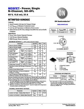
MOSFET- Power, Single N-Channel, SO-8FL 60 V, 15.6 mW, 33 A NTMFS016N06C Features Small Footprint (5x6 mm) for Compact Design www.onsemi.com Low RDS(on) to Minimize Conduction Losses Low QG and Capacitance to Minimize Driver Losses These Devices are Pb-Free, Halogen Free/BFR Free and are RoHS V(BR)DSS RDS(ON) MAX ID MAX Compliant 60 V 15.6 mW @ 10 V 33 A Applications
ntmfs4846nt1g.pdf
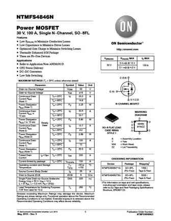
NTMFS4846N Power MOSFET 30 V, 100 A, Single N-Channel, SO-8FL Features Low RDS(on) to Minimize Conduction Losses Low Capacitance to Minimize Driver Losses Optimized Gate Charge to Minimize Switching Losses http //onsemi.com Thermally Enhanced SO8 Package These are Pb-Free Devices V(BR)DSS RDS(ON) MAX ID MAX Applications 3.4 mW @ 10 V Refer to Application Not
ntmfs4c029n.pdf
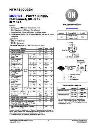
NTMFS4C029N MOSFET Power, Single, N-Channel, SO-8 FL 30 V, 46 A Features Low RDS(on) to Minimize Conduction Losses www.onsemi.com Low Capacitance to Minimize Driver Losses Optimized Gate Charge to Minimize Switching Losses V(BR)DSS RDS(ON) MAX ID MAX These Devices are Pb-Free, Halogen Free/BFR Free and are RoHS 5.88 mW @ 10 V Compliant 30 V 46 A 9.0 mW @ 4.5 V
ntmfs4c05n.pdf

NTMFS4C05N Power MOSFET 30 V, 78 A, Single N-Channel, SO-8 FL Features Low RDS(on) to Minimize Conduction Losses Low Capacitance to Minimize Driver Losses www.onsemi.com Optimized Gate Charge to Minimize Switching Losses These Devices are Pb-Free, Halogen Free/BFR Free and are RoHS Compliant V(BR)DSS RDS(ON) MAX ID MAX Applications 3.4 mW @ 10 V 30 V 78 A CPU P
ntmfs5h419nl.pdf

NTMFS5H419NL MOSFET Power, Single, N-Channel 40 V, 2.1 mW, 155 A Features Small Footprint (5x6 mm) for Compact Design www.onsemi.com Low RDS(on) to Minimize Conduction Losses Low QG and Capacitance to Minimize Driver Losses These Devices are Pb-Free and are RoHS Compliant V(BR)DSS RDS(ON) MAX ID MAX 2.1 mW @ 10 V 40 V MAXIMUM RATINGS (TJ = 25 C unless otherwise
ntmfs5830nl.pdf
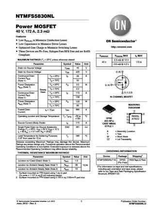
NTMFS5830NL Power MOSFET 40 V, 172 A, 2.3 mW Features Low RDS(on) to Minimize Conduction Losses Low Capacitance to Minimize Driver Losses http //onsemi.com Optimized Gate Charge to Minimize Switching Losses These Devices are Pb-Free, Halogen Free/BFR Free and are RoHS Compliant V(BR)DSS RDS(ON) MAX ID MAX MAXIMUM RATINGS (TJ = 25 C unless otherwise stated) 2.3 mW @
ntmfs4941n.pdf
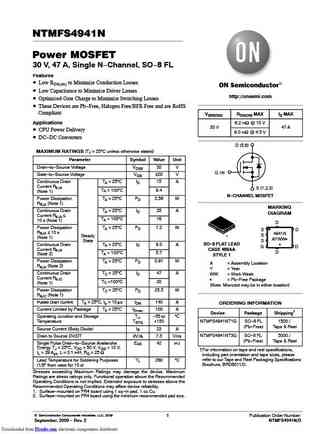
NTMFS4941N Power MOSFET 30 V, 47 A, Single N-Channel, SO-8 FL Features Low RDS(on) to Minimize Conduction Losses Low Capacitance to Minimize Driver Losses http //onsemi.com Optimized Gate Charge to Minimize Switching Losses These Devices are Pb-Free, Halogen Free/BFR Free and are RoHS Compliant V(BR)DSS RDS(ON) MAX ID MAX Applications 6.2 mW @ 10 V 30 V 47 A CPU
ntmfs5c406n.pdf
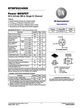
NTMFS5C406N Power MOSFET 40 V, 0.8 mW, 353 A, Single N-Channel Features Small Footprint (5x6 mm) for Compact Design Low RDS(on) to Minimize Conduction Losses www.onsemi.com Low QG and Capacitance to Minimize Driver Losses These Devices are Pb-Free and are RoHS Compliant V(BR)DSS RDS(ON) MAX ID MAX MAXIMUM RATINGS (TJ = 25 C unless otherwise noted) 40 V 0.8 mW @ 10 V
ntmfs4108n.pdf
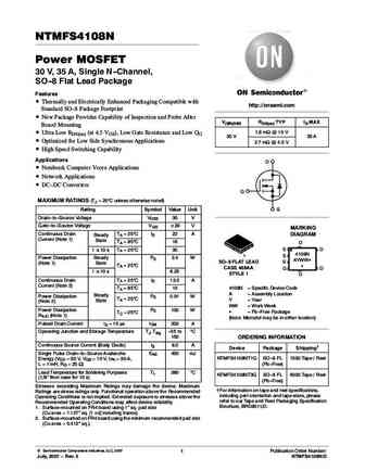
NTMFS4108N Power MOSFET 30 V, 35 A, Single N-Channel, SO-8 Flat Lead Package http //onsemi.com Features Thermally and Electrically Enhanced Packaging Compatible with http //onsemi.com Standard SO-8 Package Footprint New Package Provides Capability of Inspection and Probe After V(BR)DSS RDS(on) TYP ID MAX Board Mounting 1.8 mW @ 10 V Ultra Low RDS(on) (at 4.5 VGS), Low G
ntmfs5834nlt1g.pdf
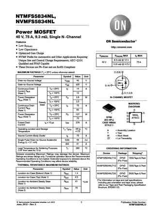
NTMFS5834NL, NVMFS5834NL Power MOSFET 40 V, 75 A, 9.3 mW, Single N-Channel Features Low RDS(on) http //onsemi.com Low Capacitance Optimized Gate Charge V(BR)DSS RDS(ON) MAX ID MAX NVMF Prefix for Automotive and Other Applications Requiring 9.3 mW @ 10 V Unique Site and Control Change Requirements; AEC-Q101 40 V 75 A Qualified and PPAP Capable 13.6 mW @ 4.5 V
ntmfs4939n-d.pdf
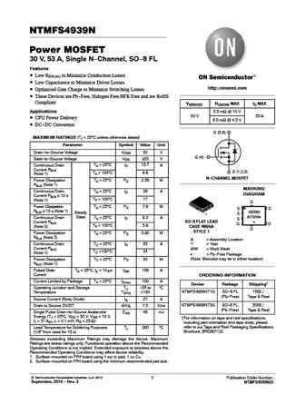
NTMFS4939N Power MOSFET 30 V, 53 A, Single N-Channel, SO-8 FL Features Low RDS(on) to Minimize Conduction Losses Low Capacitance to Minimize Driver Losses http //onsemi.com Optimized Gate Charge to Minimize Switching Losses These Devices are Pb-Free, Halogen Free/BFR Free and are RoHS Compliant V(BR)DSS RDS(ON) MAX ID MAX Applications 5.5 mW @ 10 V 30 V 53 A CP
ntmfs4845n.pdf

NTMFS4845N Power MOSFET 30 V, 115 A, Single N-Channel, SO-8FL Features Low RDS(on) to Minimize Conduction Losses Low Capacitance to Minimize Driver Losses Optimized Gate Charge to Minimize Switching Losses http //onsemi.com Thermally Enhanced SO-8 Package These are Pb-Free Devices* V(BR)DSS RDS(ON) MAX ID MAX Applications 2.9 mW @ 10 V Refer to Application N
ntmfs4c10n.pdf

NTMFS4C10N Power MOSFET 30 V, 46 A, Single N-Channel, SO-8 FL Features Low RDS(on) to Minimize Conduction Losses Low Capacitance to Minimize Driver Losses Optimized Gate Charge to Minimize Switching Losses www.onsemi.com These Devices are Pb-Free, Halogen Free/BFR Free and are RoHS Compliant V(BR)DSS RDS(ON) MAX ID MAX Applications 6.95 mW @ 10 V CPU Power Delive
ntmfsc0d9n04cl.pdf
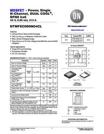
MOSFET - Power, Single N-Channel, DUAL COOL), DFN8 5x6 40 V, 0.85 mW, 313 A NTMFSC0D9N04CL www.onsemi.com Features Advanced Dual-Sided Cooled Packaging VSSS RSS(ON) MAX ID MAX Ultra Low RDS(on) to Minimize Conduction Losses 0.85 mW @ 10 V MSL1 Robust Packaging Design 40 V 313 A These Devices are Pb-Free, Halogen Free/BFR Free and are RoHS 1.3 mW @ 4.5 V Compliant
ntmfs4837nt1g.pdf
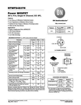
NTMFS4837N Power MOSFET 30 V, 74 A, Single N-Channel, SO-8FL Features Low RDS(on) to Minimize Conduction Losses Low Capacitance to Minimize Driver Losses http //onsemi.com Optimized Gate Charge to Minimize Switching Losses These are Pb-Free Devices Applications V(BR)DSS RDS(ON) MAX ID MAX Refer to Application Note AND8195/D 5.0 mW @ 10 V CPU Power Delivery 3
ntmfs5c612nl.pdf
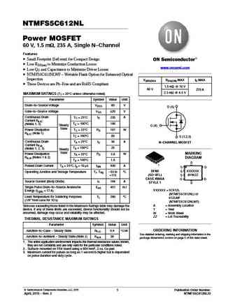
NTMFS5C612NL Power MOSFET 60 V, 1.5 mW, 235 A, Single N-Channel Features Small Footprint (5x6 mm) for Compact Design Low RDS(on) to Minimize Conduction Losses www.onsemi.com Low QG and Capacitance to Minimize Driver Losses NTMFS5C612NLWF - Wettable Flank Option for Enhanced Optical Inspection V(BR)DSS RDS(ON) MAX ID MAX These Devices are Pb-Free and are RoHS Compl
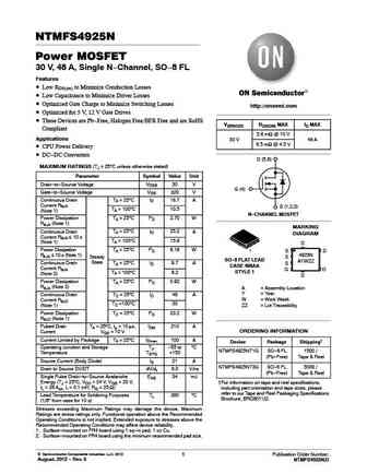
ntmfs4925n.pdf
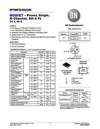
NTMFS4925N MOSFET Power, Single, N-Channel, SO-8 FL 30 V, 48 A Features Low RDS(on) to Minimize Conduction Losses http //onsemi.com Low Capacitance to Minimize Driver Losses Optimized Gate Charge to Minimize Switching Losses V(BR)DSS RDS(ON) MAX ID MAX Optimized for 5 V, 12 V Gate Drives 5.6 mW @ 10 V These Devices are Pb-Free, Halogen Free/BFR Free and are R
ntmfs4c020n.pdf
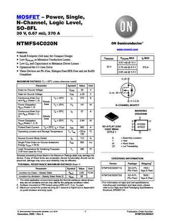
MOSFET Power, Single, N-Channel, Logic Level, SO-8FL 30 V, 0.67 mW, 370 A NTMFS4C020N www.onsemi.com Features Small Footprint (5x6 mm) for Compact Design V(BR)DSS RDS(ON) MAX ID MAX Low RDS(on) to Minimize Conduction Losses 0.67 mW @ 10 V Low QG and Capacitance to Minimize Driver Losses 30 V 0.78 mW @ 6.5 V 370 A Optimized for 4.5 Gate Drive These Devices
ntmfs5c682nl.pdf
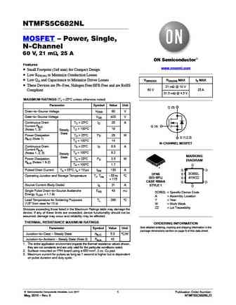
NTMFS5C682NL MOSFET Power, Single, N-Channel 60 V, 21 mW, 25 A Features www.onsemi.com Small Footprint (5x6 mm) for Compact Design Low RDS(on) to Minimize Conduction Losses Low QG and Capacitance to Minimize Driver Losses V(BR)DSS RDS(ON) MAX ID MAX These Devices are Pb-Free, Halogen Free/BFR Free and are RoHS 21 mW @ 10 V 60 V 25 A Compliant 31.5 mW @ 4.5 V MA
ntmfs4744nt1g.pdf
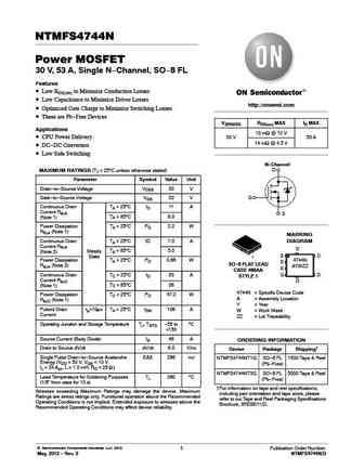
NTMFS4744N Power MOSFET 30 V, 53 A, Single N-Channel, SO-8 FL Features Low RDS(on) to Minimize Conduction Losses Low Capacitance to Minimize Driver Losses http //onsemi.com Optimized Gate Charge to Minimize Switching Losses These are Pb-Free Devices V(BR)DSS RDS(on) MAX ID MAX Applications 10 mW @ 10 V CPU Power Delivery 30 V 53 A 14 mW @ 4.5 V DC-DC Conver
ntmfs4925nt1g.pdf
NTMFS4925N Power MOSFET 30 V, 48 A, Single N-Channel, SO-8 FL Features Low RDS(on) to Minimize Conduction Losses Low Capacitance to Minimize Driver Losses Optimized Gate Charge to Minimize Switching Losses http //onsemi.com Optimized for 5 V, 12 V Gate Drives These Devices are Pb-Free, Halogen Free/BFR Free and are RoHS V(BR)DSS RDS(ON) MAX ID MAX Compliant 5.6 m
ntmfs4835nt1g.pdf
NTMFS4835N Power MOSFET 30 V, 104 A, Single N-Channel, SO-8FL Features Low RDS(on) to Minimize Conduction Losses Low Capacitance to Minimize Driver Losses http //onsemi.com Optimized Gate Charge to Minimize Switching Losses These are Pb-Free Devices V(BR)DSS RDS(ON) MAX ID MAX Applications 3.5 mW @ 10 V Refer to Application Note AND8195/D 30 V 104 A CPU Po
ntmfs4927n ntmfs4927nc.pdf
NTMFS4927N, NTMFS4927NC MOSFET Power, Single, N-Channel, SO-8 FL 30 V, 38 A Features http //onsemi.com Low RDS(on) to Minimize Conduction Losses Low Capacitance to Minimize Driver Losses Optimized Gate Charge to Minimize Switching Losses V(BR)DSS RDS(ON) MAX ID MAX Optimized for 5 V, 12 V Gate Drives 7.3 mW @ 10 V 30 V 38 A These Devices are Pb-Free, Haloge
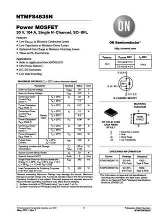
ntmfs4839nht1g.pdf
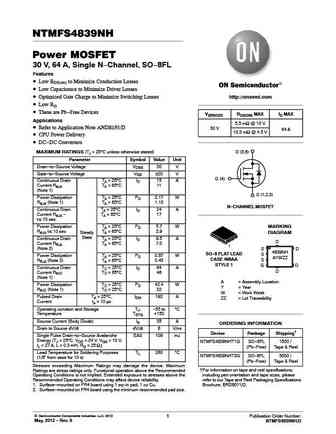
NTMFS4839NH Power MOSFET 30 V, 64 A, Single N-Channel, SO-8FL Features Low RDS(on) to Minimize Conduction Losses Low Capacitance to Minimize Driver Losses Optimized Gate Charge to Minimize Switching Losses http //onsemi.com Low RG These are Pb-Free Devices V(BR)DSS RDS(ON) MAX ID MAX Applications 5.5 mW @ 10 V Refer to Application Note AND8195/D 30 V 64 A
ntmfs5c468nl.pdf
NTMFS5C468NL MOSFET Power, Single, N-Channel 40 V, 10.3 mW, 37 A Features Small Footprint (5x6 mm) for Compact Design www.onsemi.com Low RDS(on) to Minimize Conduction Losses Low QG and Capacitance to Minimize Driver Losses V(BR)DSS RDS(ON) MAX ID MAX These Devices are Pb-Free and are RoHS Compliant 10.3 mW @ 10 V 40 V 37 A MAXIMUM RATINGS (TJ = 25 C unless ot
ntmfs4936nt1g.pdf
NTMFS4936N, NTMFS4936NC Power MOSFET 30 V, 79 A, Single N-Channel, SO-8 FL Features Low RDS(on), Low Capacitance and Optimized Gate Charge to Minimize Conduction, Driver and Switching Losses http //onsemi.com Next Generation Enhanced Body Diode, Engineered for Soft Recovery, Provides Schottky-Like Performance V(BR)DSS RDS(ON) MAX ID MAX These Devices are Pb-Free, Halogen
ntmfs4c09nt1g.pdf

NTMFS4C09N Power MOSFET 30 V, 52 A, Single N-Channel, SO-8 FL Features Low RDS(on) to Minimize Conduction Losses Low Capacitance to Minimize Driver Losses www.onsemi.com Optimized Gate Charge to Minimize Switching Losses These Devices are Pb-Free, Halogen Free/BFR Free and are RoHS V(BR)DSS RDS(ON) MAX ID MAX Compliant 5.8 mW @ 10 V Applications 30 V 52 A 8.5 mW @
ntmfs4839nt1g.pdf
NTMFS4839N Power MOSFET 30 V, 66 A, Single N-Channel, SO-8FL Features Low RDS(ON) to Minimize Conduction Losses Low Capacitance to Minimize Driver Losses http //onsemi.com Optimized Gate Charge to Minimize Switching Losses These are Pb-Free Devices V(BR)DSS RDS(ON) MAX ID MAX Applications 5.5 mW @ 10 V Refer to Application Note AND8195/D 30 V 66 A 9.5 mW @ 4.5
ntmfs5113pl.pdf
NTMFS5113PL Power MOSFET -60 V, 14 mW, -64 A, Single P-Channel Features Low RDS(on) to Minimize Conduction Losses High Current Capability www.onsemi.com Avalanche Energy Specified These Devices are Pb-Free, Halogen Free/BFR Free and are RoHS Compliant V(BR)DSS RDS(on) ID 14 mW @ -10 V MAXIMUM RATINGS (TJ = 25 C unless otherwise noted) -60 V -64 A 22 mW @ -4.5 V P
ntmfs4c03n.pdf
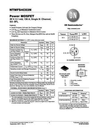
NTMFS4C03N Power MOSFET 30 V, 2.1 mW, 136 A, Single N-Channel, SO-8FL Features Small Footprint (5x6 mm) for Compact Design http //onsemi.com Low RDS(on) to Minimize Conduction Losses Low QG and Capacitance to Minimize Driver Losses V(BR)DSS RDS(ON) MAX ID MAX These Devices are Pb-Free, Halogen Free/BFR Free and are RoHS Compliant 2.1 mW @ 10 V 30 V 136 A 2.8 mW @
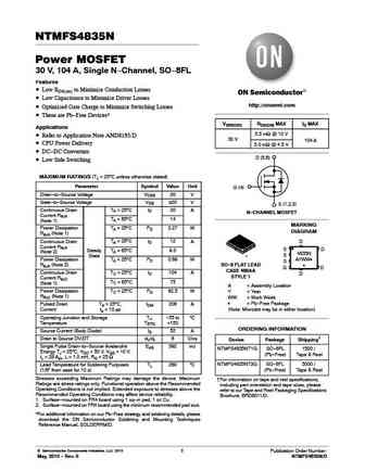
ntmfs5h431nl.pdf
NTMFS5H431NL MOSFET Power, Single, N-Channel 40 V, 3.3 mW, 106 A Features Small Footprint (5x6 mm) for Compact Design www.onsemi.com Low RDS(on) to Minimize Conduction Losses Low QG and Capacitance to Minimize Driver Losses These Devices are Pb-Free and are RoHS Compliant V(BR)DSS RDS(ON) MAX ID MAX 3.3 mW @ 10 V 40 V MAXIMUM RATINGS (TJ = 25 C unless otherwise
ntmfs5c410n.pdf

MOSFET Single, N-Channel 40 V, 0.92 mW, 300 A NTMFS5C410N Features www.onsemi.com Small Footprint (5x6 mm) for Compact Design Low RDS(on) to Minimize Conduction Losses Low QG and Capacitance to Minimize Driver Losses V(BR)DSS RDS(ON) MAX ID MAX These Devices are Pb-Free and are RoHS Compliant 40 V 0.92 mW @ 10 V 300 A MAXIMUM RATINGS (TJ = 25 C unless otherwise
ntmfs4933n.pdf

NTMFS4933N Power MOSFET 30 V, 210 A, Single N-Channel, SO-8 FL Features Low RDS(on) to Improve Conduction and Overall Efficiency These Devices are Pb-Free, Halogen Free/BFR Free and are RoHS http //onsemi.com Compliant Applications V(BR)DSS RDS(ON) MAX ID MAX OR-ing FET, Power Load Switch, Motor Control Refer to Application Note AND8195/D for Mounting Information 1.2
ntmfs5834nl nvmfs5834nl.pdf
NTMFS5834NL, NVMFS5834NL Power MOSFET 40 V, 75 A, 9.3 mW, Single N-Channel Features Low RDS(on) Low Capacitance http //onsemi.com Optimized Gate Charge NVMFS5834NLWF - Wettable Flanks Product V(BR)DSS RDS(ON) MAX ID MAX NVMFS Prefix for Automotive and Other Applications Requiring 9.3 mW @ 10 V Unique Site and Control Change Requirements; AEC-Q101 40 V 75 A 13.6
ntmfs4835n.pdf
NTMFS4835N Power MOSFET 30 V, 104 A, Single N-Channel, SO-8FL Features Low RDS(on) to Minimize Conduction Losses Low Capacitance to Minimize Driver Losses http //onsemi.com Optimized Gate Charge to Minimize Switching Losses These are Pb-Free Devices* V(BR)DSS RDS(ON) MAX ID MAX Applications 3.5 mW @ 10 V Refer to Application Note AND8195/D 30 V 104 A CPU P
ntmfs5c442n.pdf

NTMFS5C442N Power MOSFET 40 V, 2.3 mW, 140 A, Single N-Channel Features Small Footprint (5x6 mm) for Compact Design Low RDS(on) to Minimize Conduction Losses www.onsemi.com Low QG and Capacitance to Minimize Driver Losses These Devices are Pb-Free and are RoHS Compliant V(BR)DSS RDS(ON) MAX ID MAX MAXIMUM RATINGS (TJ = 25 C unless otherwise noted) Parameter Symbol Va
ntmfs5c450nl.pdf
NTMFS5C450NL Power MOSFET 40 V, 2.8 mW, 110 A, Single N-Channel Features Small Footprint (5x6 mm) for Compact Design Low RDS(on) to Minimize Conduction Losses Low QG and Capacitance to Minimize Driver Losses www.onsemi.com These Devices are Pb-Free and are RoHS Compliant V(BR)DSS RDS(ON) MAX ID MAX MAXIMUM RATINGS (TJ = 25 C unless otherwise noted) 2.8 mW @ 10 V Par
ntmfs4926n.pdf
NTMFS4926N MOSFET Power, Single, N-Channel, SO-8 FL 30 V, 44 A Features Low RDS(on) to Minimize Conduction Losses http //onsemi.com Low Capacitance to Minimize Driver Losses Optimized Gate Charge to Minimize Switching Losses V(BR)DSS RDS(ON) MAX ID MAX Optimized for 5 V, 12 V Gate Drives 7.0 mW @ 10 V These Devices are Pb-Free, Halogen Free/BFR Free and are R
ntmfs4c13n.pdf
NTMFS4C13N Power MOSFET 30 V, 38 A, Single N-Channel, SO-8 FL Features Low RDS(on) to Minimize Conduction Losses Low Capacitance to Minimize Driver Losses Optimized Gate Charge to Minimize Switching Losses http //onsemi.com These Devices are Pb-Free, Halogen Free/BFR Free and are RoHS Compliant V(BR)DSS RDS(ON) MAX ID MAX Applications 9.1 mW @ 10 V CPU Power Del
ntmfs4899nf.pdf
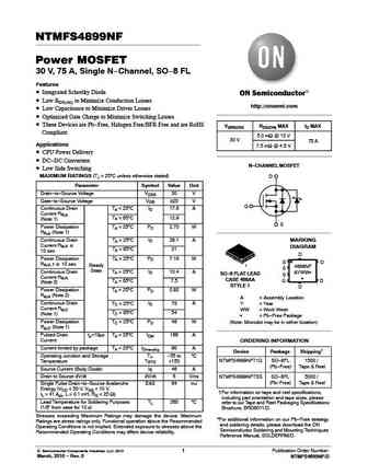
NTMFS4899NF Power MOSFET 30 V, 75 A, Single N-Channel, SO-8 FL Features Integrated Schottky Diode Low RDS(on) to Minimize Conduction Losses http //onsemi.com Low Capacitance to Minimize Driver Losses Optimized Gate Charge to Minimize Switching Losses These Devices are Pb-Free, Halogen Free/BFR Free and are RoHS V(BR)DSS RDS(ON) MAX ID MAX Compliant 5.0 mW @ 10 V
ntmfs5c450n.pdf
NTMFS5C450N MOSFET Power, Single, N-Channel 40 V, 3.3 mW, 102 A Features www.onsemi.com Small Footprint (5x6 mm) for Compact Design Low RDS(on) to Minimize Conduction Losses Low QG and Capacitance to Minimize Driver Losses V(BR)DSS RDS(ON) MAX ID MAX These Devices are Pb-Free and are RoHS Compliant 40 V 3.3 mW @ 10 V 102 A MAXIMUM RATINGS (TJ = 25 C unless other
ntmfs4c08n.pdf
NTMFS4C08N Power MOSFET 30 V, 52 A, Single N-Channel, SO-8 FL Features Low RDS(on) to Minimize Conduction Losses Low Capacitance to Minimize Driver Losses Optimized Gate Charge to Minimize Switching Losses www.onsemi.com These Devices are Pb-Free, Halogen Free/BFR Free and are RoHS Compliant Applications V(BR)DSS RDS(ON) MAX ID MAX CPU Power Delivery 5.8 mW @ 10
ntmfs4934n.pdf

NTMFS4934N Power MOSFET 30 V, 147 A, Single N-Channel, SO-8 FL Features Low RDS(on) to Minimize Conduction Losses Low Capacitance to Minimize Driver Losses http //onsemi.com Optimized Gate Charge to Minimize Switching Losses These Devices are Pb-Free, Halogen Free/BFR Free and are RoHS V(BR)DSS RDS(ON) MAX ID MAX Compliant 2.0 mW @ 10 V Applications 30 V 147 A 3.0
ntmfs4c35n.pdf
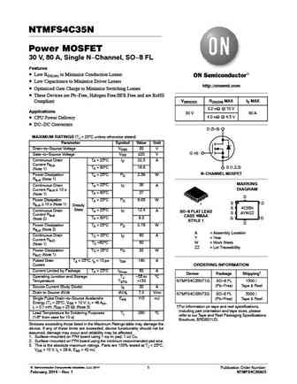
NTMFS4C35N Power MOSFET 30 V, 80 A, Single N-Channel, SO-8 FL Features Low RDS(on) to Minimize Conduction Losses Low Capacitance to Minimize Driver Losses http //onsemi.com Optimized Gate Charge to Minimize Switching Losses These Devices are Pb-Free, Halogen Free/BFR Free and are RoHS V(BR)DSS RDS(ON) MAX ID MAX Compliant 3.2 mW @ 10 V Applications 30 V 80 A 4.0 mW
ntmfs4925ne.pdf

NTMFS4925NE Power MOSFET 30 V, 48 A, Single N-Channel, SO-8 FL Features Low RDS(on) to Minimize Conduction Losses Low Capacitance to Minimize Driver Losses Optimized Gate Charge to Minimize Switching Losses http //onsemi.com Dual Sided Cooling Capability Optimized for 5 V, 12 V Gate Drives V(BR)DSS RDS(ON) MAX ID MAX These Devices are Pb-Free, Halogen Free/BFR
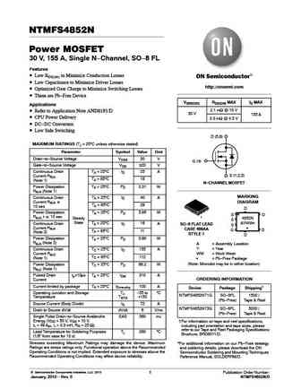
ntmfs4852nt1g.pdf
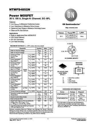
NTMFS4852N Power MOSFET 30 V, 155 A, Single N-Channel, SO-8FL Features Low RDS(on) to Minimize Conduction Losses Low Capacitance to Minimize Driver Losses http //onsemi.com Optimized Gate Charge to Minimize Switching Losses These are Pb-Free Devices V(BR)DSS RDS(ON) MAX ID MAX Applications 2.1 mW @ 10 V Refer to Application Note AND8195/D 30 V 155 A CPU Po
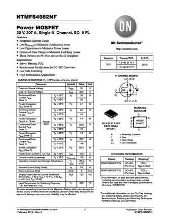
ntmfs4701n.pdf
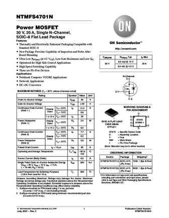
NTMFS4701N Power MOSFET 30 V, 20 A, Single N-Channel, SOIC-8 Flat Lead Package Features Thermally and Electrically Enhanced Packaging Compatible with Standard SOIC-8 http //onsemi.com New Package Provides Capability of Inspection and Probe After Board Mounting V(BR)DSS RDS(on) Typ ID Max Ultra Low RDS(on) (at 4.5 VGS), Low Gate Resistance and Low QG 6.0 mW @ 10 V O
ntmfs5c442nl.pdf
NTMFS5C442NL Power MOSFET 40 V, 2.8 mW, 121 A, Single N-Channel Features Small Footprint (5x6 mm) for Compact Design Low RDS(on) to Minimize Conduction Losses Low QG and Capacitance to Minimize Driver Losses http //onsemi.com These Devices are Pb-Free and are RoHS Compliant V(BR)DSS RDS(ON) MAX ID MAX MAXIMUM RATINGS (TJ = 25 C unless otherwise noted) 2.8 mW @ 10 V
ntmfs4982nf.pdf
NTMFS4982NF Power MOSFET 30 V, 207 A, Single N-Channel, SO-8 FL Features Integrated Schottky Diode Low RDS(on) to Minimize Conduction Losses Low Capacitance to Minimize Driver Losses http //onsemi.com Optimized Gate Charge to Minimize Switching Losses These Devices are Pb-Free and are RoHS Compliant V(BR)DSS RDS(ON) MAX ID MAX Applications 1.3 mW @ 10 V Serv
ntmfs4c025n.pdf
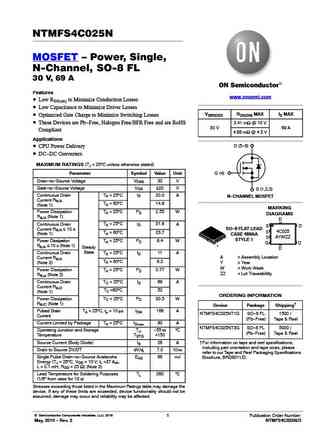
NTMFS4C025N MOSFET Power, Single, N-Channel, SO-8 FL 30 V, 69 A Features www.onsemi.com Low RDS(on) to Minimize Conduction Losses Low Capacitance to Minimize Driver Losses V(BR)DSS RDS(ON) MAX ID MAX Optimized Gate Charge to Minimize Switching Losses These Devices are Pb-Free, Halogen Free/BFR Free and are RoHS 3.41 mW @ 10 V 30 V 69 A Compliant 4.88 mW @ 4.5 V
ntmfs4708n ntmfs4708nt1g.pdf
NTMFS4708N Power MOSFET 30 V, 19 A, Single N-Channel, SOIC-8 FL Features Fast Switching Times Low Gate Charge http //onsemi.com Low RDS(on) Low Inductance SOIC-8 Package V(BR)DSS RDS(on) Typ ID Max These are Pb-Free Devices Applications 7.3 mW @ 10 V 30 V 19 A Notebooks, Graphics Cards 10.1 mW @ 4.5 V DC-DC Converters Synchronous Rectification N
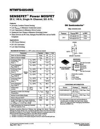
ntmfs4854nst1g.pdf

NTMFS4854NS SENSEFET Power MOSFET 25 V, 149 A, Single N-Channel, SO-8 FL Features Accurate, Lossless Current Sensing Low RDS(on) to Minimize Conduction Losses http //onsemi.com Low Capacitance to Minimize Driver Losses Optimized Gate Charge to Minimize Switching Losses V(BR)DSS RDS(ON) MAX ID MAX These Devices are Pb-Free, Halogen Free/BFR Free and are RoHS 2.5
ntmfs4h01nf.pdf
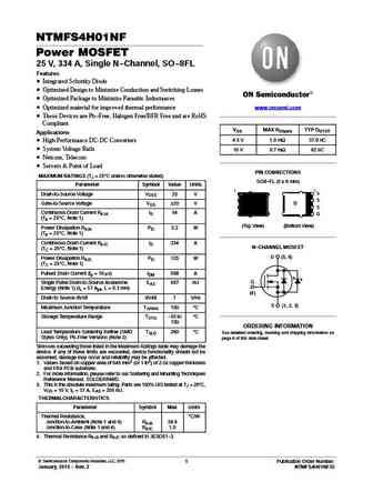
NTMFS4H01NF Power MOSFET 25 V, 334 A, Single N-Channel, SO-8FL Features Integrated Schottky Diode Optimized Design to Minimize Conduction and Switching Losses Optimized Package to Minimize Parasitic Inductances Optimized material for improved thermal performance www.onsemi.com These Devices are Pb-Free, Halogen Free/BFR Free and are RoHS Compliant VGS MAX RDS(on) T
ntmfs4939n.pdf
NTMFS4939N MOSFET Power, Single, N-Channel, SO-8 FL 30 V, 53 A Features http //onsemi.com Low RDS(on) to Minimize Conduction Losses Low Capacitance to Minimize Driver Losses Optimized Gate Charge to Minimize Switching Losses V(BR)DSS RDS(ON) MAX ID MAX These Devices are Pb-Free, Halogen Free/BFR Free and are RoHS 5.5 mW @ 10 V Compliant 30 V 53 A 8.0 mW @ 4.5 V
ntmfs5c604nl.pdf

NTMFS5C604NL Power MOSFET 60 V, 1.2 mW, 287 A, Single N-Channel Features Small Footprint (5x6 mm) for Compact Design Low RDS(on) to Minimize Conduction Losses www.onsemi.com Low QG and Capacitance to Minimize Driver Losses These Devices are Pb-Free and are RoHS Compliant V(BR)DSS RDS(ON) MAX ID MAX MAXIMUM RATINGS (TJ = 25 C unless otherwise noted) 1.2 mW @ 10 V 60
ntmfs5844nl.pdf
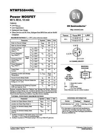
NTMFS5844NL Power MOSFET 60 V, 60 A, 12 mW Features Low RDS(on) Low Capacitance http //onsemi.com Optimized Gate Charge These Devices are Pb-Free, Halogen Free/BFR Free and are RoHS Compliant V(BR)DSS RDS(ON) MAX ID MAX MAXIMUM RATINGS (TJ = 25 C unless otherwise stated) 12 mW @ 10 V 60 V 60 A Parameter Symbol Value Unit 16 mW @ 4.5 V Drain-to-Source Voltage VDS
ntmfs5c646n.pdf
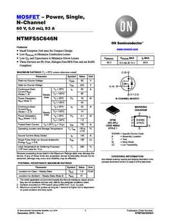
MOSFET Power, Single, N-Channel 60 V, 5.0 mW, 93 A NTMFS5C646N Features www.onsemi.com Small Footprint (5x6 mm) for Compact Design Low RDS(on) to Minimize Conduction Losses V(BR)DSS RDS(ON) MAX ID MAX Low QG and Capacitance to Minimize Driver Losses These Devices are Pb-Free, Halogen Free/BFR Free and are RoHS 60 V 5.0 mW @ 10 V 93 A Compliant MAXIMUM RATINGS (T

ntmfs5h400nl.pdf

NTMFS5H400NL MOSFET Power, Single, N-Channel 40 V, 0.80 mW, 330 A Features Small Footprint (5x6 mm) for Compact Design www.onsemi.com Low RDS(on) to Minimize Conduction Losses Low QG and Capacitance to Minimize Driver Losses V(BR)DSS RDS(ON) MAX ID MAX These Devices are Pb-Free and are RoHS Compliant 0.80 mW @ 10 V 40 V 330 A MAXIMUM RATINGS (TJ = 25 C unless
ntmfs4837nht1g.pdf
NTMFS4837NH Power MOSFET 30 V, 75 A, Single N-Channel, SO-8FL Features Low RDS(on) to Minimize Conduction Losses Low Capacitance to Minimize Driver Losses http //onsemi.com Optimized Gate Charge to Minimize Switching Losses Low RG V(BR)DSS RDS(ON) MAX ID MAX These are Pb-Free Devices 5.0 mW @ 10 V 30 V 75 A Applications 8.0 mW @ 4.5 V Refer to Application
ntmfs4h02nf.pdf
NTMFS4H02NF Power MOSFET 25 V, 193 A, Single N-Channel, SO-8FL Features Integrated Schottky Diode Optimized Design to Minimize Conduction and Switching Losses Optimized Package to Minimize Parasitic Inductances www.onsemi.com Optimized material for improved thermal performance These Devices are Pb-Free, Halogen Free/BFR Free and are RoHS Compliant VGS MAX RDS(on)
ntmfs6h836nl.pdf

MOSFET - Power, Single N-Channel 80 V, 6.2 mW, 77 A NTMFS6H836NL Features www.onsemi.com Small Footprint (5x6 mm) for Compact Design Low RDS(on) to Minimize Conduction Losses Low QG and Capacitance to Minimize Driver Losses V(BR)DSS RDS(ON) MAX ID MAX These Devices are Pb-Free and are RoHS Compliant 6.2 mW @ 10 V 80 V MAXIMUM RATINGS (TJ = 25 C unless otherwise not
ntmfs4933nt1g.pdf
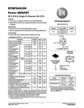
NTMFS4933N Power MOSFET 30 V, 210 A, Single N-Channel, SO-8 FL Features Low RDS(on) to Improve Conduction and Overall Efficiency These Devices are Pb-Free, Halogen Free/BFR Free and are RoHS http //onsemi.com Compliant Applications V(BR)DSS RDS(ON) MAX ID MAX OR-ing FET, Power Load Switch, Motor Control Refer to Application Note AND8195/D for Mounting Information 1.2
ntmfs3d6n10mcl.pdf

MOSFET - Power, Single N-Channel 100 V, 3.6 mW, 131 A NTMFS3D6N10MCL Features www.onsemi.com Small Footprint (5x6 mm) for Compact Design Low RDS(on) to Minimize Conduction Losses Low QG and Capacitance to Minimize Driver Losses V(BR)DSS RDS(ON) MAX ID MAX Primary DC-DC MOSFET 3.6 mW @ 10 V Synchronous Rectifier in DC-DC and AC-DC 100 V 131 A 5.8 mW @ 4.5 V
ntmfs4c09n.pdf
NTMFS4C09N MOSFET Power, Single, N-Channel, SO-8 FL 30 V, 52 A Features www.onsemi.com Low RDS(on) to Minimize Conduction Losses Low Capacitance to Minimize Driver Losses V(BR)DSS RDS(ON) MAX ID MAX Optimized Gate Charge to Minimize Switching Losses These Devices are Pb-Free, Halogen Free/BFR Free and are RoHS 5.8 mW @ 10 V 30 V 52 A Compliant 8.5 mW @ 4.5 V A
ntmfs020n06c.pdf

MOSFET- Power, Single N-Channel, SO8FL 60 V, 19.6 mW, 28 A NTMFS020N06C Features Small Footprint (5x6 mm) for Compact Design www.onsemi.com Low RDS(on) to Minimize Conduction Losses Low QG and Capacitance to Minimize Driver Losses These Devices are Pb-Free, Halogen Free/BFR Free and are RoHS V(BR)DSS RDS(ON) MAX ID MAX Compliant 60 V 19.6 mW @ 10 V 28 A Applications
ntmfs4897nft1g.pdf
NTMFS4897NF Power MOSFET 30 V, 171 A, Single N-Channel, SO-8 FL Features Low RDS(on) to Minimize Conduction Losses http //onsemi.com Low Capacitance to Minimize Driver Losses Includes Schottky Diode Optimized Gate Charge to Minimize Switching Losses V(BR)DSS RDS(ON) MAX ID MAX These are Pb-Free Device 2.0 mW @ 10 V 30 V 171 A Applications 3.0 mW @ 4.5 V C
ntmfs4852n.pdf
NTMFS4852N Power MOSFET 30 V, 155 A, Single N-Channel, SO-8 FL Features Low RDS(on) to Minimize Conduction Losses Low Capacitance to Minimize Driver Losses http //onsemi.com Optimized Gate Charge to Minimize Switching Losses These are Pb-Free Device V(BR)DSS RDS(ON) MAX ID MAX Applications 2.1 mW @ 10 V Refer to Application Note AND8195/D 30 V 155 A CPU Po
ntmfs5c430nl.pdf
NTMFS5C430NL MOSFET Power, Single, N-Channel 40 V, 1.4 mW, 200 A Features www.onsemi.com Small Footprint (5x6 mm) for Compact Design Low RDS(on) to Minimize Conduction Losses Low QG and Capacitance to Minimize Driver Losses V(BR)DSS RDS(ON) MAX ID MAX These Devices are Pb-Free and are RoHS Compliant 1.4 mW @ 10 V 40 V 200 A 2.2 mW @ 4.5 V MAXIMUM RATINGS (TJ =
ntmfs5c670n.pdf

MOSFET Power, Single, N-Channel 60 V, 7.0 mW, 71 A NTMFS5C670N Features www.onsemi.com Small Footprint (5x6 mm) for Compact Design Low RDS(on) to Minimize Conduction Losses Low QG and Capacitance to Minimize Driver Losses V(BR)DSS RDS(ON) MAX ID MAX These Devices are Pb-Free and are RoHS Compliant 60 V 7.0 mW @ 10 V 71 A MAXIMUM RATINGS (TJ = 25 C unless otherwis
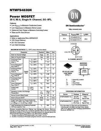
ntmfs4836n.pdf
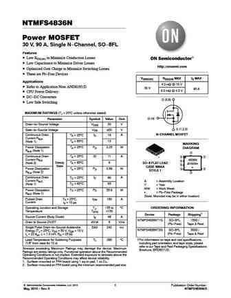
NTMFS4836N Power MOSFET 30 V, 90 A, Single N-Channel, SO-8FL Features Low RDS(on) to Minimize Conduction Losses Low Capacitance to Minimize Driver Losses http //onsemi.com Optimized Gate Charge to Minimize Switching Losses These are Pb-Free Devices V(BR)DSS RDS(ON) MAX ID MAX Applications 4.0 mW @ 10 V Refer to Application Note AND8195/D 30 V 90 A 6.0 mW @ 4.5
ntmfs0d8n02p1e.pdf
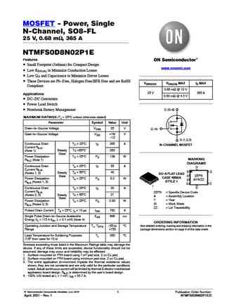
MOSFET - Power, Single N-Channel, SO8-FL 25 V, 0.68 mW, 365 A NTMFS0D8N02P1E Features Small Footprint (5x6mm) for Compact Design www.onsemi.com Low RDS(on) to Minimize Conduction Losses Low QG and Capacitance to Minimize Driver Losses These Devices are Pb-Free, Halogen Free/BFR Free and are RoHS V(BR)DSS RDS(ON) MAX ID MAX Compliant 0.68 mW @ 10 V 25 V 365 A Applic
ntmfs5h600nl.pdf
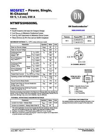
MOSFET Power, Single, N-Channel 60 V, 1.3 mW, 250 A NTMFS5H600NL Features www.onsemi.com Small Footprint (5x6 mm) for Compact Design Low RDS(on) to Minimize Conduction Losses Low QG and Capacitance to Minimize Driver Losses V(BR)DSS RDS(ON) MAX ID MAX These Devices are Pb-Free and are RoHS Compliant 1.3 mW @ 10 V 60 V 250 A MAXIMUM RATINGS (TJ = 25 C unless ot
ntmfs4839nh.pdf
NTMFS4839NH Power MOSFET 30 V, 64 A, Single N-Channel, SO-8FL Features Low RDS(ON) to Minimize Conduction Losses Low Capacitance to Minimize Driver Losses Optimized Gate Charge to Minimize Switching Losses http //onsemi.com Low RG These are Pb-Free Devices* V(BR)DSS RDS(ON) MAX ID MAX Applications 5.5 mW @ 10 V Refer to Application Note AND8195/D 30 V 64 A
ntmfs4120n.pdf
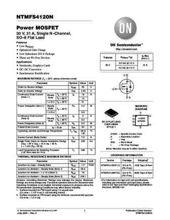
NTMFS4120N Power MOSFET 30 V, 31 A, Single N-Channel, SO-8 Flat Lead Features Low RDS(on) http //onsemi.com Optimized Gate Charge Low Inductance SO-8 Package ID Max V(BR)DSS RDS(on) Typ These are Pb-Free Devices (Note 1) Applications 3.5 mW @ 10 V 30 V 31 A Notebooks, Graphics Cards 4.2 mW @ 4.5 V DC-DC Converters Synchronous Rectification D MAXI
ntmfs6h836n.pdf
MOSFET - Power, Single N-Channel 80 V, 6.7 mW, 80 A NTMFS6H836N Features www.onsemi.com Small Footprint (5x6 mm) for Compact Design Low RDS(on) to Minimize Conduction Losses Low QG and Capacitance to Minimize Driver Losses These Devices are Pb-Free and are RoHS Compliant V(BR)DSS RDS(ON) MAX ID MAX 80 V 6.7 mW @ 10 V 80 A MAXIMUM RATINGS (TJ = 25 C unless otherwise
ntmfs4c250n.pdf
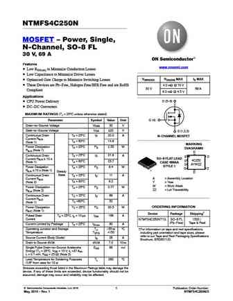
NTMFS4C250N MOSFET Power, Single, N-Channel, SO-8 FL 30 V, 69 A Features www.onsemi.com Low RDS(on) to Minimize Conduction Losses Low Capacitance to Minimize Driver Losses V(BR)DSS RDS(ON) MAX ID MAX Optimized Gate Charge to Minimize Switching Losses These Devices are Pb-Free, Halogen Free/BFR Free and are RoHS 4.0 mW @ 10 V 30 V 69 A Compliant 6.0 mW @ 4.5 V A
ntmfs6h818n.pdf
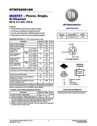
NTMFS6H818N MOSFET Power, Single, N-Channel 80 V, 3.7 mW, 123 A Features www.onsemi.com Small Footprint (5x6 mm) for Compact Design Low RDS(on) to Minimize Conduction Losses Low QG and Capacitance to Minimize Driver Losses V(BR)DSS RDS(ON) MAX ID MAX These Devices are Pb-Free and are RoHS Compliant 80 V 3.7 mW @ 10 V 123 A MAXIMUM RATINGS (TJ = 25 C unless other
ntmfs4821nt1g.pdf
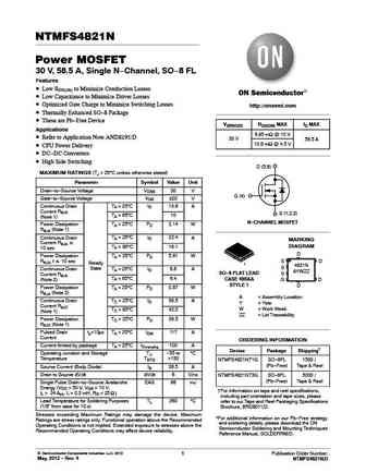
NTMFS4821N Power MOSFET 30 V, 58.5 A, Single N-Channel, SO-8 FL Features Low RDS(on) to Minimize Conduction Losses Low Capacitance to Minimize Driver Losses Optimized Gate Charge to Minimize Switching Losses http //onsemi.com Thermally Enhanced SO-8 Package These are Pb-Free Device V(BR)DSS RDS(ON) MAX ID MAX Applications 6.95 mW @ 10 V Refer to Application
ntmfs4122nt1g.pdf
NTMFS4122N Power MOSFET 30 V, 23 A, Single N-Channel, SO-8 Flat Lead Features Low RDS(on) http //onsemi.com Low Inductance SO-8 Package These are Pb-Free Devices ID MAX V(BR)DSS RDS(on) TYP (Note 1) Applications 4.6 mW @ 10 V Notebooks, Graphics Cards 30 V 23 A 6.3 mW @ 4.5 V DC-DC Converters Synchronous Rectification D MAXIMUM RATINGS (TJ = 25 C unl
ntmfs5834nl.pdf

NTMFS5834NL, NVMFS5834NL Power MOSFET 40 V, 75 A, 9.3 mW, Single N-Channel Features Low RDS(on) Low Capacitance http //onsemi.com Optimized Gate Charge NVMFS5834NLWF - Wettable Flanks Product V(BR)DSS RDS(ON) MAX ID MAX NVMFS Prefix for Automotive and Other Applications Requiring 9.3 mW @ 10 V Unique Site and Control Change Requirements; AEC-Q101 40 V 75 A 13.6
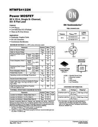
ntmfs5832nlt1g.pdf
NTMFS5832NL Power MOSFET 40 V, 111 A, 4.2 mW Features Low RDS(on) to Minimize Conduction Losses Low Capacitance to Minimize Driver Losses http //onsemi.com Optimized Gate Charge to Minimize Switching Losses These Devices are Pb-Free, Halogen Free/BFR Free and are RoHS Compliant V(BR)DSS RDS(ON) MAX ID MAX MAXIMUM RATINGS (TJ = 25 C unless otherwise stated) 4.2 mW @
ntmfs4825nfet1g.pdf
NTMFS4825NFE Power MOSFET 30 V, 171 A, Single N-Channel, SO-8 FL Features Low RDS(on) to Minimize Conduction Losses Low Capacitance to Minimize Driver Losses http //onsemi.com Includes Schottky Diode Optimized Gate Charge to Minimize Switching Losses Dual Sided Cooling Capability V(BR)DSS RDS(ON) MAX ID MAX These are Pb-Free Device 2.0 mW @ 10 V 171 A 30 V
ntmfs6h864nl.pdf
MOSFET - Power, Single N-Channel 80 V, 29 mW, 22 A NTMFS6H864NL Features www.onsemi.com Small Footprint (5x6 mm) for Compact Design Low RDS(on) to Minimize Conduction Losses Low QG and Capacitance to Minimize Driver Losses These Devices are Pb-Free and are RoHS Compliant V(BR)DSS RDS(ON) MAX ID MAX 29 mW @ 10 V MAXIMUM RATINGS (TJ = 25 C unless otherwise noted) 80
ntmfs4833nt1g.pdf
NTMFS4833N Power MOSFET 30 V, 191 A, Single N-Channel, SO-8FL Features Low RDS(on) to Minimize Conduction Losses Low Capacitance to Minimize Driver Losses http //onsemi.com Optimized Gate Charge to Minimize Switching Losses These are Pb-Free Devices V(BR)DSS RDS(ON) MAX ID MAX Applications Refer to Application Note AND8195/D 2.0 mW @ 10 V 30 V 191 A CPU Po
ntmfs4833ns.pdf

NTMFS4833NS SENSEFET) Power MOSFET 30 V, 156 A, Single N-Channel, SO-8 FL Features Accurate, Lossless Current Sensing Low RDS(on) to Minimize Conduction Losses http //onsemi.com Low Capacitance to Minimize Driver Losses Optimized Gate Charge to Minimize Switching Losses V(BR)DSS RDS(ON) MAX ID MAX These Devices are Pb-Free, Halogen Free/BFR Free and are RoHS 2.2 m
ntmfs4108nt1g.pdf
NTMFS4108N Power MOSFET 30 V, 35 A, Single N-Channel, SO-8 Flat Lead Package http //onsemi.com Features Thermally and Electrically Enhanced Packaging Compatible with http //onsemi.com Standard SO-8 Package Footprint New Package Provides Capability of Inspection and Probe After V(BR)DSS RDS(on) TYP ID MAX Board Mounting 1.8 mW @ 10 V Ultra Low RDS(on) (at 4.5 VGS), Low G
ntmfs0d55n03cg.pdf
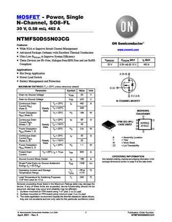
MOSFET - Power, Single N-Channel, SO8-FL 30 V, 0.58 mW, 462 A NTMFS0D55N03CG Features Wide SOA to Improve Inrush Current Management www.onsemi.com Advanced Package (5x6mm) with Excellent Thermal Conduction Ultra Low RDS(on) to Improve System Efficiency V(BR)DSS RDS(ON) MAX ID MAX These Devices are Pb-Free, Halogen Free/BFR Free and are RoHS Compliant 30 V 0.58 mW @ 1
ntmfs5c673nl.pdf
NTMFS5C673NL Power MOSFET 60 V, 9.2 mW, 50 A, Single N-Channel Features Small Footprint (5x6 mm) for Compact Design Low RDS(on) to Minimize Conduction Losses www.onsemi.com Low QG and Capacitance to Minimize Driver Losses These Devices are Pb-Free and are RoHS Compliant V(BR)DSS RDS(ON) MAX ID MAX MAXIMUM RATINGS (TJ = 25 C unless otherwise noted) 9.2 mW @ 10 V 60 V
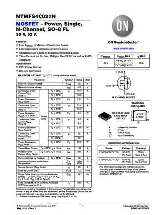
ntmfs4c032n.pdf
NTMFS4C032N MOSFET Power, Single, N-Channel, SO-8 FL 30 V, 38 A Features Low RDS(on) to Minimize Conduction Losses www.onsemi.com Low Capacitance to Minimize Driver Losses Optimized Gate Charge to Minimize Switching Losses V(BR)DSS RDS(ON) MAX ID MAX These Devices are Pb-Free, Halogen Free/BFR Free and are RoHS 7.35 mW @ 10 V Compliant 30 V 38 A Applications 1
ntmfs4c027n.pdf
NTMFS4C027N MOSFET Power, Single, N-Channel, SO-8 FL 30 V, 52 A Features Low RDS(on) to Minimize Conduction Losses www.onsemi.com Low Capacitance to Minimize Driver Losses Optimized Gate Charge to Minimize Switching Losses These Devices are Pb-Free, Halogen Free/BFR Free and are RoHS V(BR)DSS RDS(ON) MAX ID MAX Compliant 4.8 mW @ 10 V 30 V 52 A Applications 7.4
ntmfs4847n.pdf

NTMFS4847N Power MOSFET 30 V, 85 A, Single N-Channel, SO-8FL Features Low RDS(on) to Minimize Conduction Losses Low Capacitance to Minimize Driver Losses Optimized Gate Charge to Minimize Switching Losses http //onsemi.com Thermally Enhanced SO-8 Package These are Pb-Free Devices* V(BR)DSS RDS(ON) MAX ID MAX Applications 4.1 mW @ 10 V Refer to Application No
ntmfs4854ns.pdf
NTMFS4854NS SENSEFET Power MOSFET 25 V, 149 A, Single N-Channel, SO-8 FL Features Accurate, Lossless Current Sensing Low RDS(on) to Minimize Conduction Losses http //onsemi.com Low Capacitance to Minimize Driver Losses Optimized Gate Charge to Minimize Switching Losses V(BR)DSS RDS(ON) MAX ID MAX These Devices are Pb-Free, Halogen Free/BFR Free and are RoHS 2.5
ntmfs5c673n.pdf
MOSFET Power, Single, N-Channel 60 V, 10.7 mW, 50 A NTMFS5C673N Features www.onsemi.com Small Footprint (5x6 mm) for Compact Design Low RDS(on) to Minimize Conduction Losses Low QG and Capacitance to Minimize Driver Losses V(BR)DSS RDS(ON) MAX ID MAX These Devices are Pb-Free and are RoHS Compliant 60 V 10.7 mW @ 10 V 50 A MAXIMUM RATINGS (TJ = 25 C unless other
ntmfs5c460nl.pdf
NTMFS5C460NL Power MOSFET 40 V, 4.5 mW, 78 A, Single N-Channel Features Small Footprint (5x6 mm) for Compact Design Low RDS(on) to Minimize Conduction Losses www.onsemi.com Low QG and Capacitance to Minimize Driver Losses These Devices are Pb-Free and are RoHS Compliant V(BR)DSS RDS(ON) MAX ID MAX MAXIMUM RATINGS (TJ = 25 C unless otherwise noted) 4.5 mW @ 10 V 40 V
ntmfs4841nh.pdf
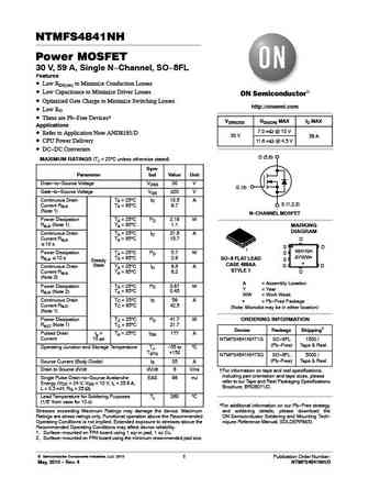
NTMFS4841NH Power MOSFET 30 V, 59 A, Single N-Channel, SO-8FL Features Low RDS(on) to Minimize Conduction Losses Low Capacitance to Minimize Driver Losses Optimized Gate Charge to Minimize Switching Losses http //onsemi.com Low RG These are Pb-Free Devices* V(BR)DSS RDS(ON) MAX ID MAX Applications 7.0 mW @ 10 V Refer to Application Note AND8195/D 30 V 59 A
ntmfs4955n.pdf
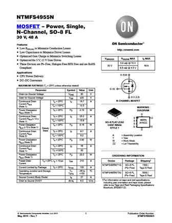
NTMFS4955N MOSFET Power, Single, N-Channel, SO-8 FL 30 V, 48 A Features Low RDS(on) to Minimize Conduction Losses http //onsemi.com Low Capacitance to Minimize Driver Losses Optimized Gate Charge to Minimize Switching Losses V(BR)DSS RDS(ON) MAX ID MAX Optimized for 5 V, 12 V Gate Drives 5.6 mW @ 10 V These Devices are Pb-Free, Halogen Free/BFR Free and are R
ntmfs4833n.pdf
NTMFS4833N Power MOSFET 30 V, 191 A, Single N-Channel, SO-8 FL Features Low RDS(on) to Minimize Conduction Losses Low Capacitance to Minimize Driver Losses Optimized Gate Charge to Minimize Switching Losses http //onsemi.com These are Pb-Free Devices* Applications V(BR)DSS RDS(ON) MAX ID MAX CPU Power Delivery DC-DC Converters 2.0 mW @ 10 V 30 V 191 A
ntmfs6h800nl.pdf
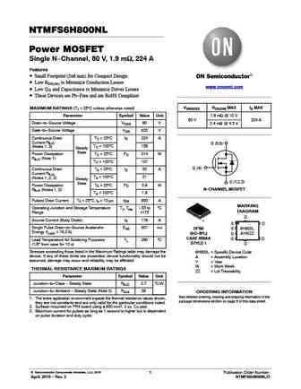
NTMFS6H800NL Power MOSFET Single N-Channel, 80 V, 1.9 mW, 224 A Features Small Footprint (5x6 mm) for Compact Design Low RDS(on) to Minimize Conduction Losses www.onsemi.com Low QG and Capacitance to Minimize Driver Losses These Devices are Pb-Free and are RoHS Compliant V(BR)DSS RDS(ON) MAX ID MAX MAXIMUM RATINGS (TJ = 25 C unless otherwise noted) Parameter Symbol V
ntmfs5844nl nvmfs5844nl.pdf
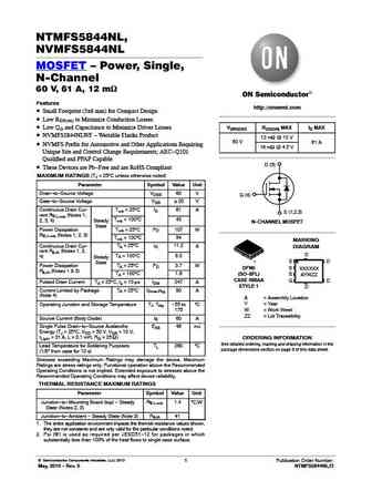
NTMFS5844NL, NVMFS5844NL MOSFET Power, Single, N-Channel 60 V, 61 A, 12 mW Features http //onsemi.com Small Footprint (5x6 mm) for Compact Design Low RDS(on) to Minimize Conduction Losses Low QG and Capacitance to Minimize Driver Losses V(BR)DSS RDS(ON) MAX ID MAX NVMFS5844NLWF - Wettable Flanks Product 12 mW @ 10 V 60 V 61 A NVMFS Prefix for Automotive and
ntmfs4923ne.pdf
NTMFS4923NE Power MOSFET 30 V, 91 A, Single N-Channel, SO-8 FL Features Low RDS(on) to Minimize Conduction Losses Low Capacitance to Minimize Driver Losses http //onsemi.com Optimized Gate Charge to Minimize Switching Losses Dual Sided Cooling Capability V(BR)DSS RDS(ON) MAX ID MAX These Devices are Pb-Free, Halogen Free and are RoHS Compliant 3.3 mW @ 10 V 91 A
ntmfs5c404nlt.pdf
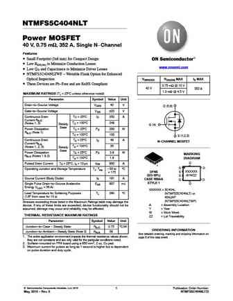
NTMFS5C404NLT Power MOSFET 40 V, 0.75 mW, 352 A, Single N-Channel Features Small Footprint (5x6 mm) for Compact Design Low RDS(on) to Minimize Conduction Losses www.onsemi.com Low QG and Capacitance to Minimize Driver Losses NTMFS5C404NLTWF - Wettable Flank Option for Enhanced Optical Inspection V(BR)DSS RDS(ON) MAX ID MAX These Devices are Pb-Free and are RoHS Co
ntmfs6h800n.pdf

NTMFS6H800N MOSFET Power, Single, N-Channel 80 V, 2.1 mW, 203 A Features www.onsemi.com Small Footprint (5x6 mm) for Compact Design Low RDS(on) to Minimize Conduction Losses Low QG and Capacitance to Minimize Driver Losses V(BR)DSS RDS(ON) MAX ID MAX These Devices are Pb-Free and are RoHS Compliant 80 V 2.1 mW @ 10 V 203 A MAXIMUM RATINGS (TJ = 25 C unless other
ntmfs5832nl.pdf

NTMFS5832NL Power MOSFET 40 V, 111 A, 4.2 mW Features Low RDS(on) to Minimize Conduction Losses Low Capacitance to Minimize Driver Losses http //onsemi.com Optimized Gate Charge to Minimize Switching Losses These Devices are Pb-Free, Halogen Free/BFR Free and are RoHS Compliant V(BR)DSS RDS(ON) MAX ID MAX MAXIMUM RATINGS (TJ = 25 C unless otherwise stated) 4.2 mW @
ntmfs5c677nl.pdf
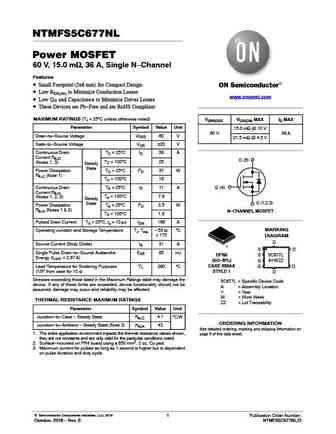
NTMFS5C677NL Power MOSFET 60 V, 15.0 mW, 36 A, Single N-Channel Features Small Footprint (5x6 mm) for Compact Design Low RDS(on) to Minimize Conduction Losses www.onsemi.com Low QG and Capacitance to Minimize Driver Losses These Devices are Pb-Free and are RoHS Compliant MAXIMUM RATINGS (TJ = 25 C unless otherwise noted) V(BR)DSS RDS(ON) MAX ID MAX Parameter Symbol V
ntmfs6h801nl.pdf

MOSFET - Power, Single N-Channel 80 V, 2.7 mW, 160 A NTMFS6H801NL Features www.onsemi.com Small Footprint (5x6 mm) for Compact Design Low RDS(on) to Minimize Conduction Losses Low QG and Capacitance to Minimize Driver Losses These Devices are Pb-Free and are RoHS Compliant V(BR)DSS RDS(ON) MAX ID MAX 2.7 mW @ 10 V MAXIMUM RATINGS (TJ = 25 C unless otherwise noted)
ntmfs4834n.pdf
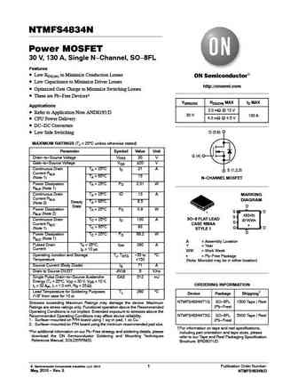
NTMFS4834N Power MOSFET 30 V, 130 A, Single N-Channel, SO-8FL Features Low RDS(on) to Minimize Conduction Losses Low Capacitance to Minimize Driver Losses http //onsemi.com Optimized Gate Charge to Minimize Switching Losses These are Pb-Free Devices* V(BR)DSS RDS(ON) MAX ID MAX Applications 3.0 mW @ 10 V Refer to Application Note AND8195/D 30 V 130 A 4.0 mW @
ntmfs4926ne.pdf
NTMFS4926NE Power MOSFET 30 V, 44 A, Single N-Channel, SO-8 FL Features Low RDS(on) to Minimize Conduction Losses Low Capacitance to Minimize Driver Losses Optimized Gate Charge to Minimize Switching Losses http //onsemi.com Dual Sided Cooling Capability Optimized for 5 V, 12 V Gate Drives V(BR)DSS RDS(ON) MAX ID MAX These Devices are Pb-Free, Halogen Free/BFR
ntmfs4898nft1g.pdf
NTMFS4898NF Power MOSFET 30 V, 117 A, Single N-Channel, SO-8FL Features Integrated Schottky Diode Low RDS(on) to Minimize Conduction Losses Low Capacitance to Minimize Driver Losses http //onsemi.com Optimized Gate Charge to Minimize Switching Losses These Devices are Pb-Free, Halogen Free/BFR Free and are RoHS V(BR)DSS RDS(ON) MAX ID MAX Compliant 3.0 mW @ 10 V
ntmfs6h848nl.pdf
MOSFET - Power, Single N-Channel 80 V, 8.8 mW, 59 A NTMFS6H848NL Features www.onsemi.com Small Footprint (5x6 mm) for Compact Design Low RDS(on) to Minimize Conduction Losses Low QG and Capacitance to Minimize Driver Losses V(BR)DSS RDS(ON) MAX ID MAX These Devices are Pb-Free and are RoHS Compliant 8.8 mW @ 10 V MAXIMUM RATINGS (TJ = 25 C unless otherwise noted) 80
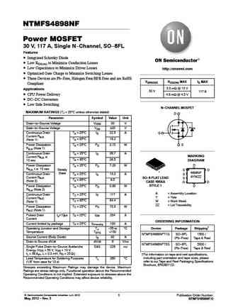
ntmfs4841n.pdf
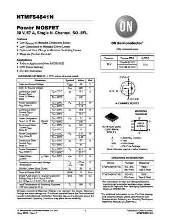
NTMFS4841N Power MOSFET 30 V, 57 A, Single N-Channel, SO-8FL Features Low RDS(on) to Minimize Conduction Losses Low Capacitance to Minimize Driver Losses http //onsemi.com Optimized Gate Charge to Minimize Switching Losses These are Pb-Free Devices* V(BR)DSS RDS(ON) MAX ID MAX Applications 7.0 mW @ 10 V Refer to Application Note AND8195/D 30 V 57 A 11.4 mW @ 4
ntmfs5h610nl.pdf

NTMFS5H610NL MOSFET Power, Single, N-Channel 60 V, 10 mW, 44 A Features Small Footprint (5x6 mm) for Compact Design www.onsemi.com Low RDS(on) to Minimize Conduction Losses Low QG and Capacitance to Minimize Driver Losses V(BR)DSS RDS(ON) MAX ID MAX These Devices are Pb-Free and are RoHS Compliant 10 mW @ 10 V 60 V 44 A MAXIMUM RATINGS (TJ = 25 C unless otherw
ntmfs4922ne.pdf
NTMFS4922NE Power MOSFET 30 V, 147 A, Single N-Channel, SO-8 FL Features Low RDS(on) to Minimize Conduction Losses Low Capacitance to Minimize Driver Losses http //onsemi.com Optimized Gate Charge to Minimize Switching Losses Dual Sided Cooling Capability V(BR)DSS RDS(ON) MAX ID MAX These Devices are Pb-Free, Halogen Free/BFR Free and are RoHS Compliant 2.0 mW @
ntmfs4119n.pdf
NTMFS4119N Power MOSFET 30 V, 30 A, Single N-Channel, SO-8 Flat Lead Features Low RDS(on) http //onsemi.com Fast Switching Times Low Inductance SO-8 Package ID Max V(BR)DSS RDS(on) Typ (Note 1) These are Pb-Free Devices 2.3 mW @ 10 V Applications 30 V 30 A 3.1 mW @ 4.5 V Notebooks, Graphics Cards Low Side Switch DC-DC D MAXIMUM RATINGS (TJ = 25 C
ntmfs5c628nl.pdf

NTMFS5C628NL Power MOSFET 60 V, 2.4 mW, 150 A, Single N-Channel Features Small Footprint (5x6 mm) for Compact Design Low RDS(on) to Minimize Conduction Losses www.onsemi.com Low QG and Capacitance to Minimize Driver Losses These Devices are Pb-Free and are RoHS Compliant V(BR)DSS RDS(ON) MAX ID MAX MAXIMUM RATINGS (TJ = 25 C unless otherwise noted) 2.4 mW @ 10 V 60
ntmfs4937nt1g.pdf
NTMFS4937N Power MOSFET 30 V, 70 A, Single N-Channel, SO-8 FL Features Low RDS(on) to Minimize Conduction Losses Low Capacitance to Minimize Driver Losses Optimized Gate Charge to Minimize Switching Losses http //onsemi.com These Devices are Pb-Free, Halogen Free/BFR Free and are RoHS Compliant V(BR)DSS RDS(ON) MAX ID MAX Applications 4.0 mW @ 10 V CPU Power Del
ntmfs4c06n.pdf
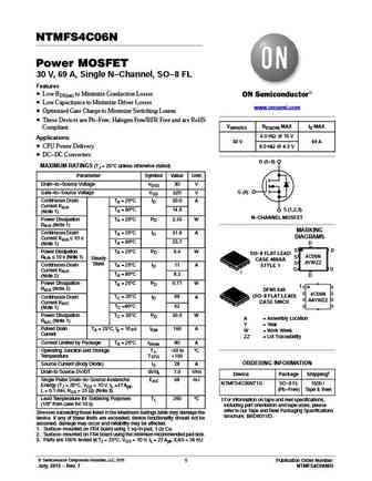
NTMFS4C06N Power MOSFET 30 V, 69 A, Single N-Channel, SO-8 FL Features Low RDS(on) to Minimize Conduction Losses Low Capacitance to Minimize Driver Losses www.onsemi.com Optimized Gate Charge to Minimize Switching Losses These Devices are Pb-Free, Halogen Free/BFR Free and are RoHS V(BR)DSS RDS(ON) MAX ID MAX Compliant 4.0 mW @ 10 V Applications 30 V 69 A CPU P
ntmfs4841nht1g.pdf
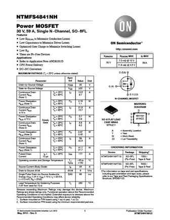
NTMFS4841NH Power MOSFET 30 V, 59 A, Single N-Channel, SO-8FL Features Low RDS(on) to Minimize Conduction Losses Low Capacitance to Minimize Driver Losses Optimized Gate Charge to Minimize Switching Losses http //onsemi.com Low RG These are Pb-Free Devices V(BR)DSS RDS(ON) MAX ID MAX Applications 7.0 mW @ 10 V Refer to Application Note AND8195/D 30 V 59 A
ntmfs6b14n.pdf

NTMFS6B14N Power MOSFET 100 V, 15 mW, 50 A, Single N-Channel Features Small Footprint (5x6 mm) for Compact Design Low RDS(on) to Minimize Conduction Losses www.onsemi.com Low QG and Capacitance to Minimize Driver Losses These Devices are Pb-Free, Halogen Free/BFR Free and are RoHS Compliant V(BR)DSS RDS(ON) MAX ID MAX MAXIMUM RATINGS (TJ = 25 C unless otherwise noted
ntmfs5c670nl.pdf
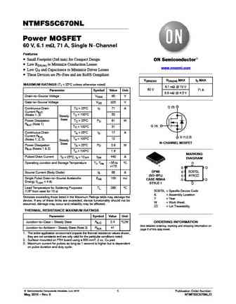
NTMFS5C670NL Power MOSFET 60 V, 6.1 mW, 71 A, Single N-Channel Features Small Footprint (5x6 mm) for Compact Design Low RDS(on) to Minimize Conduction Losses www.onsemi.com Low QG and Capacitance to Minimize Driver Losses These Devices are Pb-Free and are RoHS Compliant V(BR)DSS RDS(ON) MAX ID MAX MAXIMUM RATINGS (TJ = 25 C unless otherwise noted) 6.1 mW @ 10 V 60 V
ntmfs5c426n.pdf
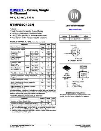
MOSFET Power, Single N-Channel 40 V, 1.3 mW, 235 A NTMFS5C426N Features www.onsemi.com Small Footprint (5x6 mm) for Compact Design Low RDS(on) to Minimize Conduction Losses Low QG and Capacitance to Minimize Driver Losses V(BR)DSS RDS(ON) MAX ID MAX These Devices are Pb-Free and are RoHS Compliant 40 V 1.3 mW @ 10 V 235 A MAXIMUM RATINGS (TJ = 25 C unless otherw
ntmfs4939nt1g.pdf

NTMFS4939N Power MOSFET 30 V, 53 A, Single N-Channel, SO-8 FL Features Low RDS(on) to Minimize Conduction Losses Low Capacitance to Minimize Driver Losses http //onsemi.com Optimized Gate Charge to Minimize Switching Losses These Devices are Pb-Free, Halogen Free/BFR Free and are RoHS Compliant V(BR)DSS RDS(ON) MAX ID MAX Applications 5.5 mW @ 10 V 30 V 53 A CP
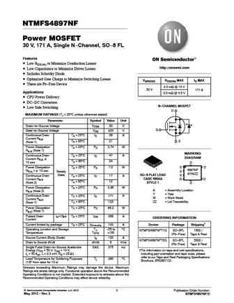
ntmfs5c456nl.pdf

MOSFET Power, Single, N-Channel 40 V, 3.7 mW, 87 A NTMFS5C456NL Features Small Footprint (5x6 mm) for Compact Design www.onsemi.com Low RDS(on) to Minimize Conduction Losses Low QG and Capacitance to Minimize Driver Losses V(BR)DSS RDS(ON) MAX ID MAX These Devices are Pb-Free and are RoHS Compliant 3.7 mW @ 10 V 40 V 87 A MAXIMUM RATINGS (TJ = 25 C unless other
ntmfs4936n-d.pdf
NTMFS4936N Power MOSFET 30 V, 79 A, Single N-Channel, SO-8 FL Features Low RDS(on), Low Capacitance and Optimized Gate Charge to Minimize Conduction, Driver and Switching Losses http //onsemi.com Next Generation Enhanced Body Diode, Engineered for Soft Recovery, Provides Schottky-Like Performance These Devices are Pb-Free, Halogen Free/BFR Free and are RoHS V(BR)DSS RDS(ON
ntmfs4823n.pdf
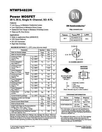
NTMFS4823N Power MOSFET 30 V, 30 A, Single N-Channel, SO-8 FL Features Low RDS(on) to Minimize Conduction Losses Low Capacitance to Minimize Driver Losses http //onsemi.com Optimized Gate Charge to Minimize Switching Losses These are Pb-Free Device V(BR)DSS RDS(ON) MAX ID MAX Applications Refer to Application Note AND8195/D 10.5 mW @ 10 V 30 V 30 A CPU Pow
ntmfs4836nt1g.pdf
NTMFS4836N Power MOSFET 30 V, 90 A, Single N-Channel, SO-8FL Features Low RDS(on) to Minimize Conduction Losses Low Capacitance to Minimize Driver Losses http //onsemi.com Optimized Gate Charge to Minimize Switching Losses These are Pb-Free Devices V(BR)DSS RDS(ON) MAX ID MAX Applications 4.0 mW @ 10 V Refer to Application Note AND8195/D 30 V 90 A 6.0 mW @ 4.5
ntmfs5c410nl.pdf
NTMFS5C410NL Power MOSFET 40 V, 0.9 mW, 302 A, Single N-Channel Features Small Footprint (5x6 mm) for Compact Design Low RDS(on) to Minimize Conduction Losses http //onsemi.com Low QG and Capacitance to Minimize Driver Losses These Devices are Pb-Free and are RoHS Compliant V(BR)DSS RDS(ON) MAX ID MAX MAXIMUM RATINGS (TJ = 25 C unless otherwise noted) 0.9 mW @ 10 V
ntmfs6b03n.pdf
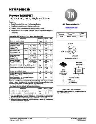
NTMFS6B03N Power MOSFET 100 V, 4.8 mW, 132 A, Single N-Channel Features Small Footprint (5x6 mm) for Compact Design Low RDS(on) to Minimize Conduction Losses www.onsemi.com Low QG and Capacitance to Minimize Driver Losses These Devices are Pb-Free, Halogen Free/BFR Free and are RoHS Compliant V(BR)DSS RDS(ON) MAX ID MAX MAXIMUM RATINGS (TJ = 25 C unless otherwise not
ntmfs5c645nl.pdf
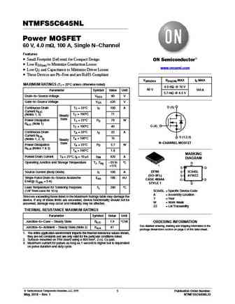
NTMFS5C645NL Power MOSFET 60 V, 4.0 mW, 100 A, Single N-Channel Features Small Footprint (5x6 mm) for Compact Design Low RDS(on) to Minimize Conduction Losses www.onsemi.com Low QG and Capacitance to Minimize Driver Losses These Devices are Pb-Free and are RoHS Compliant V(BR)DSS RDS(ON) MAX ID MAX MAXIMUM RATINGS (TJ = 25 C unless otherwise noted) 4.0 mW @ 10 V 60
ntmfs4837n-d.pdf
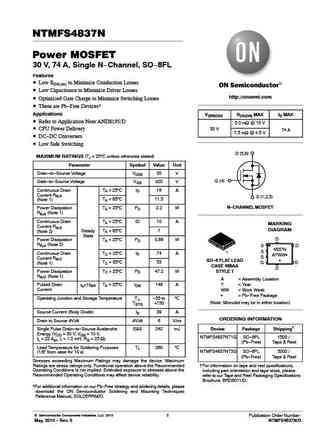
NTMFS4837N Power MOSFET 30 V, 74 A, Single N-Channel, SO-8FL Features Low RDS(on) to Minimize Conduction Losses Low Capacitance to Minimize Driver Losses http //onsemi.com Optimized Gate Charge to Minimize Switching Losses These are Pb-Free Devices* Applications V(BR)DSS RDS(ON) MAX ID MAX Refer to Application Note AND8195/D 5.0 mW @ 10 V CPU Power Delivery
ntmfs6b05n.pdf

NTMFS6B05N Power MOSFET 100 V, 8 mW, 104 A, Single N-Channel Features Small Footprint (5x6 mm) for Compact Design Low RDS(on) to Minimize Conduction Losses www.onsemi.com Low QG and Capacitance to Minimize Driver Losses These Devices are Pb-Free, Halogen Free/BFR Free and are RoHS Compliant V(BR)DSS RDS(ON) MAX ID MAX MAXIMUM RATINGS (TJ = 25 C unless otherwise noted
ntmfs4837nh.pdf
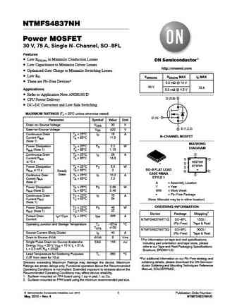
NTMFS4837NH Power MOSFET 30 V, 75 A, Single N-Channel, SO-8FL Features Low RDS(on) to Minimize Conduction Losses Low Capacitance to Minimize Driver Losses http //onsemi.com Optimized Gate Charge to Minimize Switching Losses Low RG V(BR)DSS RDS(ON) MAX ID MAX These are Pb-Free Devices* 5.0 mW @ 10 V 30 V 75 A Applications 8.0 mW @ 4.5 V Refer to Application
ntmfs4833nst1g.pdf
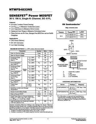
NTMFS4833NS SENSEFET) Power MOSFET 30 V, 156 A, Single N-Channel, SO-8 FL Features Accurate, Lossless Current Sensing Low RDS(on) to Minimize Conduction Losses http //onsemi.com Low Capacitance to Minimize Driver Losses Optimized Gate Charge to Minimize Switching Losses V(BR)DSS RDS(ON) MAX ID MAX These Devices are Pb-Free, Halogen Free/BFR Free and are RoHS 2.2 m
ntmfs5c423nl.pdf
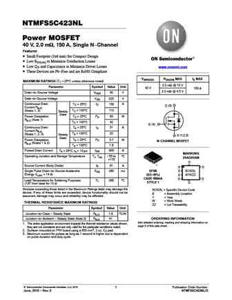
NTMFS5C423NL Power MOSFET 40 V, 2.0 mW, 150 A, Single N-Channel Features Small Footprint (5x6 mm) for Compact Design Low RDS(on) to Minimize Conduction Losses Low QG and Capacitance to Minimize Driver Losses www.onsemi.com These Devices are Pb-Free and are RoHS Compliant V(BR)DSS RDS(ON) MAX ID MAX MAXIMUM RATINGS (TJ = 25 C unless otherwise noted) 2.0 mW @ 10 V Par
ntmfs08n003c.pdf
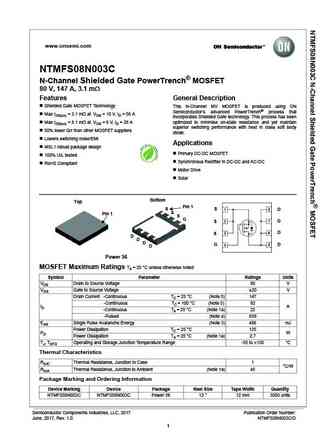
www.onsemi.com NTMFS08N003C N-Channel Shielded Gate PowerTrench MOSFET 80 V, 147 A, 3.1 m Features General Description Shielded Gate MOSFET Technology This N-Channel MV MOSFET is produced using ON Semiconductor s advanced PowerTrench process that Max rDS(on) = 3.1 m at VGS = 10 V, ID = 56 A incorporates Shielded Gate technology. This process has been Max rDS(on) = 8.1 m
ntmfs4c01n.pdf
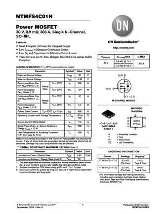
NTMFS4C01N Power MOSFET 30 V, 0.9 mW, 303 A, Single N-Channel, SO-8FL Features Small Footprint (5x6 mm) for Compact Design http //onsemi.com Low RDS(on) to Minimize Conduction Losses Low QG and Capacitance to Minimize Driver Losses V(BR)DSS RDS(ON) MAX ID MAX These Devices are Pb-Free, Halogen Free/BFR Free and are RoHS Compliant 0.9 mW @ 10 V 30 V 303 A 1.2 mW @
ntmfs4936n ntmfs4936nc.pdf
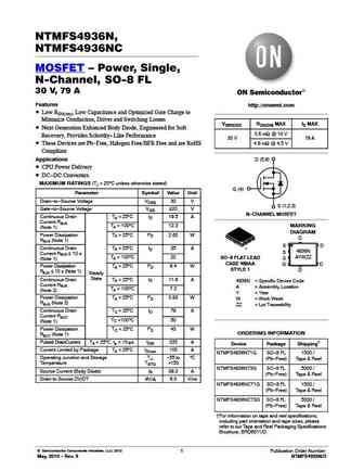
NTMFS4936N, NTMFS4936NC MOSFET Power, Single, N-Channel, SO-8 FL 30 V, 79 A Features http //onsemi.com Low RDS(on), Low Capacitance and Optimized Gate Charge to Minimize Conduction, Driver and Switching Losses V(BR)DSS RDS(ON) MAX ID MAX Next Generation Enhanced Body Diode, Engineered for Soft 3.8 mW @ 10 V Recovery, Provides Schottky-Like Performance 30 V 79 A The
ntmfs4121n.pdf
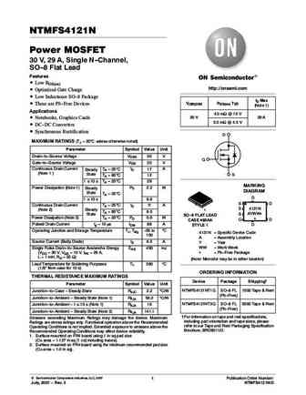
NTMFS4121N Power MOSFET 30 V, 29 A, Single N-Channel, SO-8 Flat Lead Features Low RDS(on) http //onsemi.com Optimized Gate Charge Low Inductance SO-8 Package ID Max V(BR)DSS RDS(on) Typ These are Pb-Free Devices (Note 1) Applications 4.0 mW @ 10 V 30 V 29 A Notebooks, Graphics Cards 5.5 mW @ 4.5 V DC-DC Converters Synchronous Rectification D MAXI
ntmfs4122n.pdf
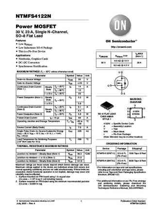
NTMFS4122N Power MOSFET 30 V, 23 A, Single N-Channel, SO-8 Flat Lead Features Low RDS(on) http //onsemi.com Low Inductance SO-8 Package This is a Pb-Free Device ID MAX Applications V(BR)DSS RDS(on) TYP (Note 1) Notebooks, Graphics Cards 4.6 mW @ 10 V DC-DC Converters 30 V 23 A 6.3 mW @ 4.5 V Synchronous Rectification MAXIMUM RATINGS (TJ = 25 C unless o
ntmfs4c028n.pdf
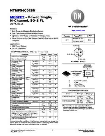
NTMFS4C028N MOSFET Power, Single, N-Channel, SO-8 FL 30 V, 52 A Features www.onsemi.com Low RDS(on) to Minimize Conduction Losses Low Capacitance to Minimize Driver Losses V(BR)DSS RDS(ON) MAX ID MAX Optimized Gate Charge to Minimize Switching Losses These Devices are Pb-Free, Halogen Free/BFR Free and are RoHS 4.73 mW @ 10 V 30 V 52 A Compliant 7.0 mW @ 4.5 V
ntmfs4897nf.pdf
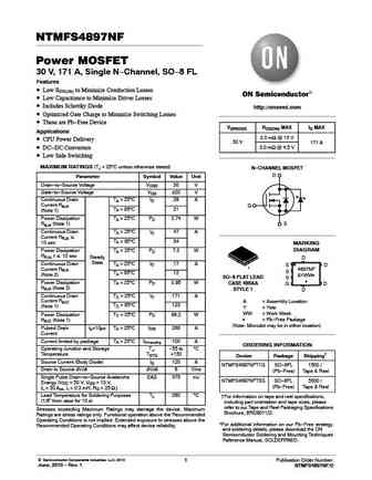
NTMFS4897NF Power MOSFET 30 V, 171 A, Single N-Channel, SO-8 FL Features Low RDS(on) to Minimize Conduction Losses Low Capacitance to Minimize Driver Losses Includes Schottky Diode http //onsemi.com Optimized Gate Charge to Minimize Switching Losses These are Pb-Free Device V(BR)DSS RDS(ON) MAX ID MAX Applications 2.0 mW @ 10 V CPU Power Delivery 30 V 171
ntmfs5c646nl.pdf
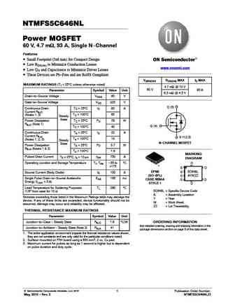
NTMFS5C646NL Power MOSFET 60 V, 4.7 mW, 93 A, Single N-Channel Features Small Footprint (5x6 mm) for Compact Design Low RDS(on) to Minimize Conduction Losses www.onsemi.com Low QG and Capacitance to Minimize Driver Losses These Devices are Pb-Free and are RoHS Compliant V(BR)DSS RDS(ON) MAX ID MAX MAXIMUM RATINGS (TJ = 25 C unless otherwise noted) 4.7 mW @ 10 V 60 V
ntmfs4935n.pdf
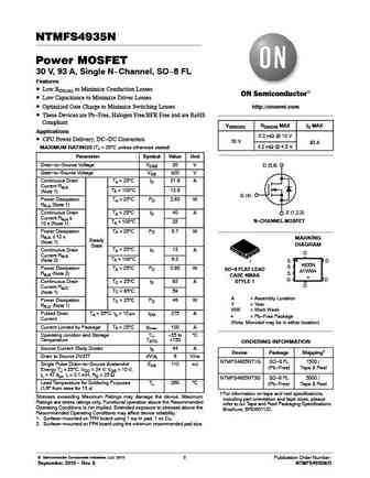
NTMFS4935N Power MOSFET 30 V, 93 A, Single N-Channel, SO-8 FL Features Low RDS(on) to Minimize Conduction Losses Low Capacitance to Minimize Driver Losses Optimized Gate Charge to Minimize Switching Losses http //onsemi.com These Devices are Pb-Free, Halogen Free/BFR Free and are RoHS Compliant V(BR)DSS RDS(ON) MAX ID MAX Applications 3.2 mW @ 10 V CPU Power Deli
ntmfs4851nt1g.pdf

NTMFS4851N Power MOSFET 30 V, 66 A, Single N-Channel, SO-8FL Features Low RDS(on) to Minimize Conduction Losses Low Capacitance to Minimize Driver Losses Optimized Gate Charge to Minimize Switching Losses http //onsemi.com Thermally Enhanced SO8 Package These are Pb-Free Devices V(BR)DSS RDS(ON) MAX ID MAX Applications 5.9 mW @ 10 V Refer to Application Note
ntmfs4119nt1g.pdf

NTMFS4119N Power MOSFET 30 V, 30 A, Single N-Channel, SO-8 Flat Lead Features Low RDS(on) http //onsemi.com Fast Switching Times Low Inductance SO-8 Package ID Max V(BR)DSS RDS(on) Typ (Note 1) These are Pb-Free Devices 2.3 mW @ 10 V Applications 30 V 30 A 3.1 mW @ 4.5 V Notebooks, Graphics Cards Low Side Switch DC-DC D MAXIMUM RATINGS (TJ = 25 C
ntmfs4121nt1g.pdf

NTMFS4121N Power MOSFET 30 V, 29 A, Single N-Channel, SO-8 Flat Lead Features Low RDS(on) http //onsemi.com Optimized Gate Charge Low Inductance SO-8 Package ID Max V(BR)DSS RDS(on) Typ (Note 1) These are Pb-Free Devices 4.0 mW @ 10 V Applications 30 V 29 A 5.5 mW @ 4.5 V Notebooks, Graphics Cards DC-DC Converters D Synchronous Rectification MAXI
ntmfs4983nf.pdf
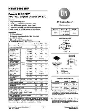
NTMFS4983NF Power MOSFET 30 V, 106 A, Single N-Channel, SO-8 FL Features Integrated Schottky Diode Low RDS(on) to Minimize Conduction Losses http //onsemi.com Low Capacitance to Minimize Driver Losses Optimized Gate Charge to Minimize Switching Losses These Devices are Pb-Free and are RoHS Compliant V(BR)DSS RDS(ON) MAX ID MAX 2.1 mW @ 10 V Applications 30 V 10
ntmfs5h630nl.pdf
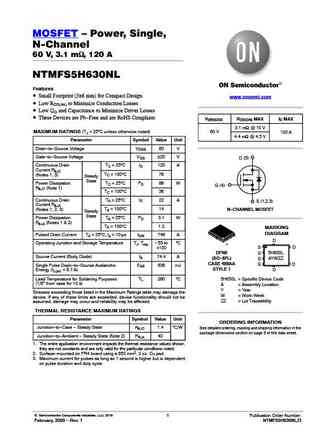
MOSFET Power, Single, N-Channel 60 V, 3.1 mW, 120 A NTMFS5H630NL Features Small Footprint (5x6 mm) for Compact Design www.onsemi.com Low RDS(on) to Minimize Conduction Losses Low QG and Capacitance to Minimize Driver Losses These Devices are Pb-Free and are RoHS Compliant V(BR)DSS RDS(ON) MAX ID MAX 3.1 mW @ 10 V MAXIMUM RATINGS (TJ = 25 C unless otherwise noted
ntmfs4921nt1g.pdf
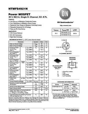
NTMFS4921N Power MOSFET 30 V, 58.5 A, Single N-Channel, SO-8 FL Features Low RDS(on) to Minimize Conduction Losses Low Capacitance to Minimize Driver Losses Optimized Gate Charge to Minimize Switching Losses http //onsemi.com Thermally Enhanced SO-8 Package These are Pb-Free Device V(BR)DSS RDS(ON) MAX ID MAX Applications 6.95 mW @ 10 V CPU Power Delivery 3
ntmfs4851n.pdf

NTMFS4851N Power MOSFET 30 V, 66 A, Single N-Channel, SO-8FL Features Low RDS(on) to Minimize Conduction Losses Low Capacitance to Minimize Driver Losses Optimized Gate Charge to Minimize Switching Losses http //onsemi.com Thermally Enhanced SO8 Package These are Pb-Free Devices* V(BR)DSS RDS(ON) MAX ID MAX Applications 5.9 mW @ 10 V Refer to Application Not
ntmfs5c609nl.pdf
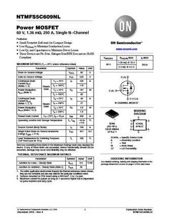
NTMFS5C609NL Power MOSFET 60 V, 1.36 mW, 250 A, Single N-Channel Features Small Footprint (5x6 mm) for Compact Design Low RDS(on) to Minimize Conduction Losses www.onsemi.com Low QG and Capacitance to Minimize Driver Losses These Devices are Pb-Free, Halogen Free/BFR Free and are RoHS Compliant V(BR)DSS RDS(ON) MAX ID MAX 1.36 mW @ 10 V MAXIMUM RATINGS (TJ = 25 C un
ntmfs4934nt1g.pdf
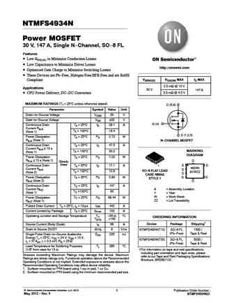
NTMFS4934N Power MOSFET 30 V, 147 A, Single N-Channel, SO-8 FL Features Low RDS(on) to Minimize Conduction Losses Low Capacitance to Minimize Driver Losses http //onsemi.com Optimized Gate Charge to Minimize Switching Losses These Devices are Pb-Free, Halogen Free/BFR Free and are RoHS V(BR)DSS RDS(ON) MAX ID MAX Compliant 2.0 mW @ 10 V Applications 30 V 147 A 3.0
ntmfs4985nf.pdf
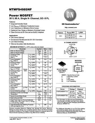
NTMFS4985NF Power MOSFET 30 V, 65 A, Single N-Channel, SO-8 FL Features Integrated Schottky Diode Low RDS(on) to Minimize Conduction Losses http //onsemi.com Low Capacitance to Minimize Driver Losses Optimized Gate Charge to Minimize Switching Losses These Devices are Pb-Free and are RoHS Compliant V(BR)DSS RDS(ON) MAX ID MAX 3.4 mW @ 10 V Applications 30 V 65
ntmfs4c024n.pdf
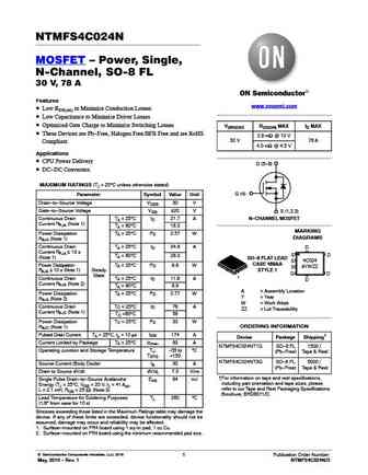
NTMFS4C024N MOSFET Power, Single, N-Channel, SO-8 FL 30 V, 78 A Features www.onsemi.com Low RDS(on) to Minimize Conduction Losses Low Capacitance to Minimize Driver Losses Optimized Gate Charge to Minimize Switching Losses V(BR)DSS RDS(ON) MAX ID MAX These Devices are Pb-Free, Halogen Free/BFR Free and are RoHS 2.8 mW @ 10 V 30 V 78 A Compliant 4.0 mW @ 4.5 V
ntmfs4931n.pdf
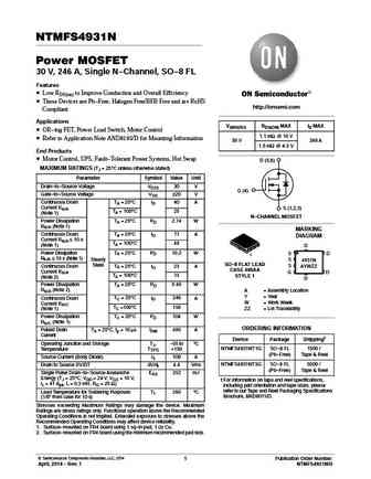
NTMFS4931N Power MOSFET 30 V, 246 A, Single N-Channel, SO-8 FL Features Low RDS(on) to Improve Conduction and Overall Efficiency These Devices are Pb-Free, Halogen Free/BFR Free and are RoHS http //onsemi.com Compliant Applications V(BR)DSS RDS(ON) MAX ID MAX OR-ing FET, Power Load Switch, Motor Control 1.1 mW @ 10 V Refer to Application Note AND8195/D for Mounting I
ntmfs6d1n08h.pdf
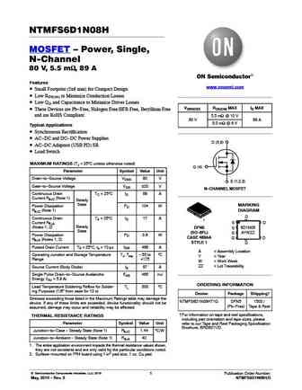
NTMFS6D1N08H MOSFET Power, Single, N-Channel 80 V, 5.5 mW, 89 A Features www.onsemi.com Small Footprint (5x6 mm) for Compact Design Low RDS(on) to Minimize Conduction Losses Low QG and Capacitance to Minimize Driver Losses V(BR)DSS RDS(ON) MAX ID MAX These Devices are Pb-Free, Halogen Free/BFR Free, Beryllium Free and are RoHS Compliant 5.5 mW @ 10 V 80 V 89 A
ntmfs5830nlt1g.pdf

NTMFS5830NL Power MOSFET 40 V, 172 A, 2.3 mW Features Low RDS(on) to Minimize Conduction Losses Low Capacitance to Minimize Driver Losses http //onsemi.com Optimized Gate Charge to Minimize Switching Losses These Devices are Pb-Free, Halogen Free/BFR Free and are RoHS Compliant V(BR)DSS RDS(ON) MAX ID MAX MAXIMUM RATINGS (TJ = 25 C unless otherwise stated) 2.3 mW @
ntmfs5h409nl.pdf
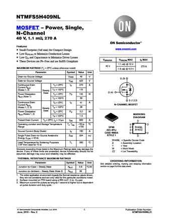
NTMFS5H409NL MOSFET Power, Single, N-Channel 40 V, 1.1 mW, 270 A Features www.onsemi.com Small Footprint (5x6 mm) for Compact Design Low RDS(on) to Minimize Conduction Losses Low QG and Capacitance to Minimize Driver Losses V(BR)DSS RDS(ON) MAX ID MAX These Devices are Pb-Free and are RoHS Compliant 1.1 mW @ 10 V 40 V 270 A MAXIMUM RATINGS (TJ = 25 C unless ot
ntmfs4941nt1g.pdf
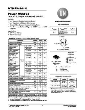
NTMFS4941N Power MOSFET 30 V, 47 A, Single N-Channel, SO-8 FL Features Low RDS(on) to Minimize Conduction Losses Low Capacitance to Minimize Driver Losses http //onsemi.com Optimized Gate Charge to Minimize Switching Losses These Devices are Pb-Free, Halogen Free/BFR Free and are RoHS Compliant V(BR)DSS RDS(ON) MAX ID MAX Applications 6.2 mW @ 10 V 30 V 47 A CP
ntmfs4h01n.pdf

NTMFS4H01N Power MOSFET 25 V, 334 A, Single N-Channel, SO-8FL Features Optimized Design to Minimize Conduction and Switching Losses Optimized Package to Minimize Parasitic Inductances Optimized material for improved thermal performance http //onsemi.com These Devices are Pb-Free, Halogen Free/BFR Free and are RoHS Compliant VGS MAX RDS(on) TYP QGTOT Applications
ntmfs6h818nl.pdf

MOSFET - Power, Single N-Channel 80 V, 3.2 mW, 135 A NTMFS6H818NL Features www.onsemi.com Small Footprint (5x6 mm) for Compact Design Low RDS(on) to Minimize Conduction Losses Low QG and Capacitance to Minimize Driver Losses These Devices are Pb-Free and are RoHS Compliant V(BR)DSS RDS(ON) MAX ID MAX 3.2 mW @ 10 V MAXIMUM RATINGS (TJ = 25 C unless otherwise noted)
ntmfs5c404nl.pdf
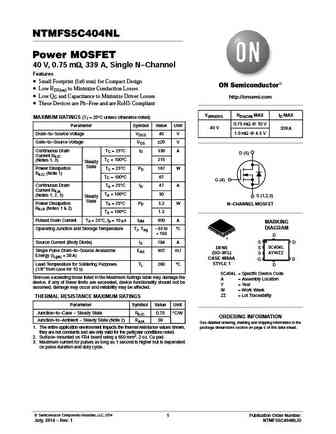
NTMFS5C404NL Power MOSFET 40 V, 0.75 mW, 339 A, Single N-Channel Features Small Footprint (5x6 mm) for Compact Design Low RDS(on) to Minimize Conduction Losses Low QG and Capacitance to Minimize Driver Losses http //onsemi.com These Devices are Pb-Free and are RoHS Compliant V(BR)DSS RDS(ON) MAX ID MAX MAXIMUM RATINGS (TJ = 25 C unless otherwise noted) 0.75 mW @ 10 V
ntmfs4823nt1g.pdf
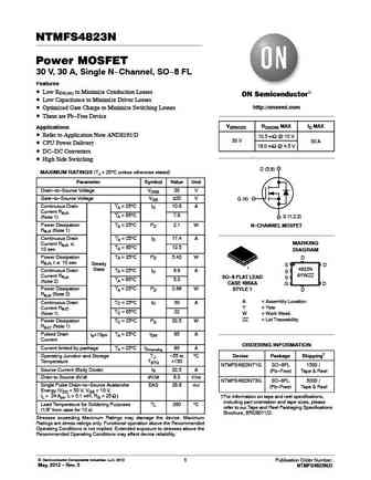
NTMFS4823N Power MOSFET 30 V, 30 A, Single N-Channel, SO-8 FL Features Low RDS(on) to Minimize Conduction Losses Low Capacitance to Minimize Driver Losses http //onsemi.com Optimized Gate Charge to Minimize Switching Losses These are Pb-Free Device V(BR)DSS RDS(ON) MAX ID MAX Applications Refer to Application Note AND8195/D 10.5 mW @ 10 V 30 V 30 A CPU Pow
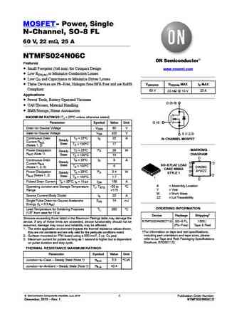
ntmfs4921n.pdf
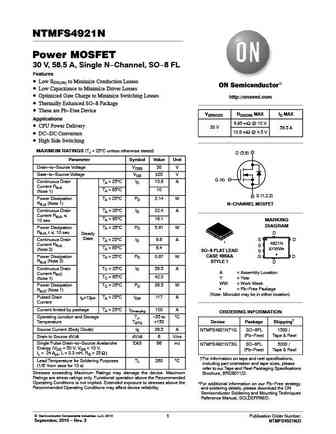
NTMFS4921N Power MOSFET 30 V, 58.5 A, Single N-Channel, SO-8 FL Features Low RDS(on) to Minimize Conduction Losses Low Capacitance to Minimize Driver Losses Optimized Gate Charge to Minimize Switching Losses http //onsemi.com Thermally Enhanced SO-8 Package These are Pb-Free Device V(BR)DSS RDS(ON) MAX ID MAX Applications 6.95 mW @ 10 V CPU Power Delivery 3
ntmfs4946n.pdf
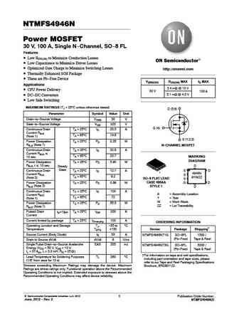
NTMFS4946N Power MOSFET 30 V, 100 A, Single N-Channel, SO-8 FL Features Low RDS(on) to Minimize Conduction Losses Low Capacitance to Minimize Driver Losses Optimized Gate Charge to Minimize Switching Losses http //onsemi.com Thermally Enhanced SO8 Package These are Pb-Free Device V(BR)DSS RDS(ON) MAX ID MAX Applications 3.4 mW @ 10 V CPU Power Delivery 30 V
ntmfs6h852nl.pdf

MOSFET - Power, Single N-Channel 80 V, 13.1 mW, 42 A NTMFS6H852NL Features www.onsemi.com Small Footprint (5x6 mm) for Compact Design Low RDS(on) to Minimize Conduction Losses Low QG and Capacitance to Minimize Driver Losses V(BR)DSS RDS(ON) MAX ID MAX These Devices are Pb-Free and are RoHS Compliant 13.1 mW @ 10 V MAXIMUM RATINGS (TJ = 25 C unless otherwise noted)
ntmfs4841nt1g.pdf
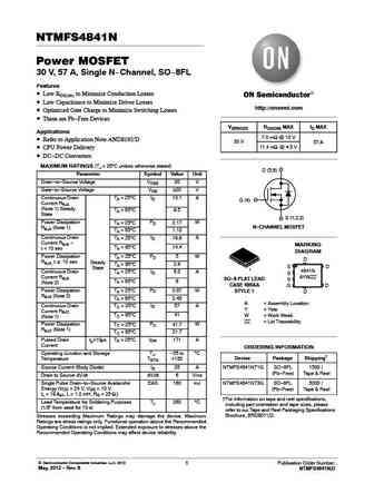
NTMFS4841N Power MOSFET 30 V, 57 A, Single N-Channel, SO-8FL Features Low RDS(on) to Minimize Conduction Losses Low Capacitance to Minimize Driver Losses http //onsemi.com Optimized Gate Charge to Minimize Switching Losses These are Pb-Free Devices V(BR)DSS RDS(ON) MAX ID MAX Applications 7.0 mW @ 10 V Refer to Application Note AND8195/D 30 V 57 A 11.4 mW @ 4.
ntmfs4935nbt1g ntmfs4935nct1g ntmfs4935nt1g.pdf
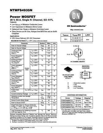
NTMFS4935N Power MOSFET 30 V, 93 A, Single N-Channel, SO-8 FL Features Low RDS(on) to Minimize Conduction Losses Low Capacitance to Minimize Driver Losses Optimized Gate Charge to Minimize Switching Losses http //onsemi.com These Devices are Pb-Free, Halogen Free/BFR Free and are RoHS Compliant V(BR)DSS RDS(ON) MAX ID MAX Applications 3.2 mW @ 10 V CPU Power Del
ntmfs5c404n.pdf
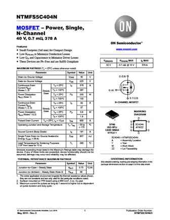
NTMFS5C404N MOSFET Power, Single, N-Channel 40 V, 0.7 mW, 378 A Features www.onsemi.com Small Footprint (5x6 mm) for Compact Design Low RDS(on) to Minimize Conduction Losses Low QG and Capacitance to Minimize Driver Losses V(BR)DSS RDS(ON) MAX ID MAX These Devices are Pb-Free and are RoHS Compliant 40 V 0.7 mW @ 10 V 378 A MAXIMUM RATINGS (TJ = 25 C unless other
ntmfs4898nf.pdf
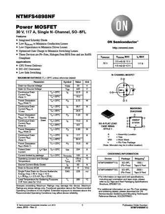
NTMFS4898NF Power MOSFET 30 V, 117 A, Single N-Channel, SO-8FL Features Integrated Schottky Diode Low RDS(on) to Minimize Conduction Losses Low Capacitance to Minimize Driver Losses http //onsemi.com Optimized Gate Charge to Minimize Switching Losses These Devices are Pb-Free, Halogen Free/BFR Free and are RoHS V(BR)DSS RDS(ON) MAX ID MAX Compliant 3.0 mW @ 10 V
ntmfs4943n.pdf

NTMFS4943N Power MOSFET 30 V, 41 A, Single N-Channel, SO-8 FL Features Low RDS(on) to Minimize Conduction Losses Low Capacitance to Minimize Driver Losses Optimized Gate Charge to Minimize Switching Losses http //onsemi.com These Devices are Pb-Free, Halogen Free/BFR Free and are RoHS Compliant V(BR)DSS RDS(ON) MAX ID MAX Applications 7.2 mW @ 10 V CPU Power Deli
ntmfs4849n.pdf
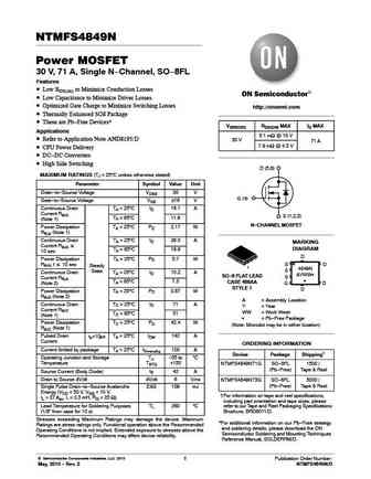
NTMFS4849N Power MOSFET 30 V, 71 A, Single N-Channel, SO-8FL Features Low RDS(on) to Minimize Conduction Losses Low Capacitance to Minimize Driver Losses Optimized Gate Charge to Minimize Switching Losses http //onsemi.com Thermally Enhanced SO8 Package These are Pb-Free Devices* V(BR)DSS RDS(ON) MAX ID MAX Applications 5.1 mW @ 10 V Refer to Application Not
ntmfs5844nlt1g nvmfs5844nl.pdf
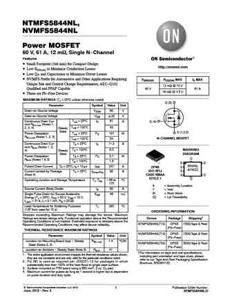
NTMFS5844NL, NVMFS5844NL Power MOSFET 60 V, 61 A, 12 mW, Single N-Channel Features Small Footprint (5x6 mm) for Compact Design http //onsemi.com Low RDS(on) to Minimize Conduction Losses Low QG and Capacitance to Minimize Driver Losses NVMFS Prefix for Automotive and Other Applications Requiring V(BR)DSS RDS(ON) MAX ID MAX Unique Site and Control Change Requirements;
ntmfs5c406nl.pdf
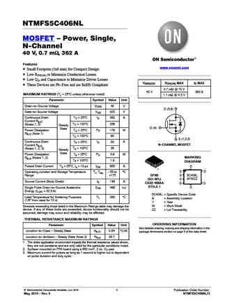
NTMFS5C406NL MOSFET Power, Single, N-Channel 40 V, 0.7 mW, 362 A Features www.onsemi.com Small Footprint (5x6 mm) for Compact Design Low RDS(on) to Minimize Conduction Losses Low QG and Capacitance to Minimize Driver Losses V(BR)DSS RDS(ON) MAX ID MAX These Devices are Pb-Free and are RoHS Compliant 0.7 mW @ 10 V 40 V 362 A MAXIMUM RATINGS (TJ = 25 C unless oth
ntmfs0d9n03cg.pdf
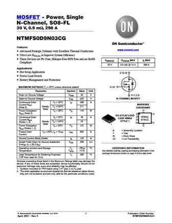
MOSFET - Power, Single N-Channel, SO8-FL 30 V, 0.9 mW, 298 A NTMFS0D9N03CG Features www.onsemi.com Advanced Package (5x6mm) with Excellent Thermal Conduction Ultra Low RDS(on) to Improve System Efficiency These Devices are Pb-Free, Halogen Free/BFR Free and are RoHS V(BR)DSS RDS(ON) MAX ID MAX Compliant 30 V 0.9 mW @ 10 V 298 A Applications Hot Swap Application D (
ntmfs4821n.pdf
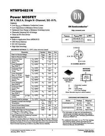
NTMFS4821N Power MOSFET 30 V, 58.5 A, Single N-Channel, SO-8 FL Features Low RDS(on) to Minimize Conduction Losses Low Capacitance to Minimize Driver Losses Optimized Gate Charge to Minimize Switching Losses http //onsemi.com Thermally Enhanced SO-8 Package These are Pb-Free Device V(BR)DSS RDS(ON) MAX ID MAX Applications 6.95 mW @ 10 V Refer to Application
ntmfs4c302n.pdf
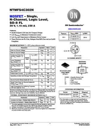
NTMFS4C302N MOSFET Single, N-Channel, Logic Level, SO-8 FL 30 V, 1.15 mW, 230 A www.onsemi.com Features Small Footprint (5x6 mm) for Compact Design V(BR)DSS RDS(on) MAX ID MAX Low RDS(on) to Minimize Conduction Losses 1.15 mW @ 10 V Low QG and Capacitance to Minimize Driver Losses 30 V 230 A 1.7 mW @ 4.5 V These Devices are Pb-Free, Halogen Free/BFR Free and a
ntmfs5c628n.pdf
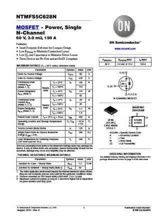
NTMFS5C628N MOSFET - Power, Single N-Channel 60 V, 3.0 mW, 150 A Features Small Footprint (5x6 mm) for Compact Design www.onsemi.com Low RDS(on) to Minimize Conduction Losses Low QG and Capacitance to Minimize Driver Losses These Devices are Pb-Free and are RoHS Compliant V(BR)DSS RDS(ON) MAX ID MAX 60 V 3.0 mW @ 10 V 150 A MAXIMUM RATINGS (TJ = 25 C unless otherwis
ntmfs23d9n06hl.pdf
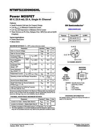
NTMFS23D9N06HL Power MOSFET 60 V, 23.9 mW, 23 A, Single N-Channel Features Small Footprint (5x6 mm) for Compact Design Low RDS(on) to Minimize Conduction Losses www.onsemi.com Low QG and Capacitance to Minimize Driver Losses These Devices are Pb-Free, Halogen-Free / BFR Free and are RoHS Compliant V(BR)DSS RDS(ON) MAX ID MAX Typical Applications 23.9 mW @ 10 V 60 V
ntmfs5h615nl.pdf
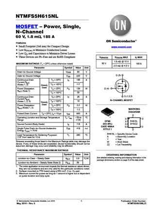
NTMFS5H615NL MOSFET Power, Single, N-Channel 60 V, 1.8 mW, 185 A Features Small Footprint (5x6 mm) for Compact Design www.onsemi.com Low RDS(on) to Minimize Conduction Losses Low QG and Capacitance to Minimize Driver Losses These Devices are Pb-Free and are RoHS Compliant V(BR)DSS RDS(ON) MAX ID MAX 1.8 mW @ 10 V 60 V MAXIMUM RATINGS (TJ = 25 C unless otherwise
ntmfs5c442nlt.pdf
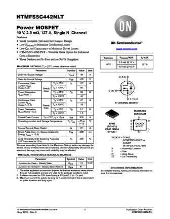
NTMFS5C442NLT Power MOSFET 40 V, 2.8 mW, 127 A, Single N-Channel Features Small Footprint (5x6 mm) for Compact Design Low RDS(on) to Minimize Conduction Losses Low QG and Capacitance to Minimize Driver Losses www.onsemi.com NTMFS5C442NLTWF - Wettable Flank Option for Enhanced Optical Inspection V(BR)DSS RDS(ON) MAX ID MAX These Devices are Pb-Free and are RoHS Com
ntmfs4926n-d.pdf

NTMFS4926N Power MOSFET 30 V, 44 A, Single N-Channel, SO-8 FL Features Low RDS(on) to Minimize Conduction Losses Low Capacitance to Minimize Driver Losses Optimized Gate Charge to Minimize Switching Losses http //onsemi.com Optimized for 5 V, 12 V Gate Drives These Devices are Pb-Free, Halogen Free/BFR Free and are RoHS V(BR)DSS RDS(ON) MAX ID MAX Compliant 7.0 m
ntmfs4937n.pdf
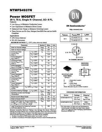
NTMFS4937N Power MOSFET 30 V, 70 A, Single N-Channel, SO-8 FL Features Low RDS(on) to Minimize Conduction Losses Low Capacitance to Minimize Driver Losses Optimized Gate Charge to Minimize Switching Losses http //onsemi.com These Devices are Pb-Free, Halogen Free/BFR Free and are RoHS Compliant V(BR)DSS RDS(ON) MAX ID MAX Applications 4.5 mW @ 10 V CPU Power Del
ntmfs5h414nl.pdf
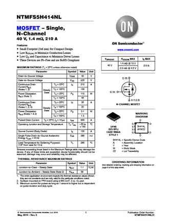
NTMFS5H414NL MOSFET Single, N-Channel 40 V, 1.4 mW, 210 A Features Small Footprint (5x6 mm) for Compact Design www.onsemi.com Low RDS(on) to Minimize Conduction Losses Low QG and Capacitance to Minimize Driver Losses V(BR)DSS RDS(ON) MAX ID MAX These Devices are Pb-Free and are RoHS Compliant 1.4 mW @ 10 V 40 V 210 A MAXIMUM RATINGS (TJ = 25 C unless otherwise
ntmfs4h02n.pdf
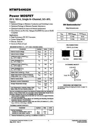
NTMFS4H02N Power MOSFET 25 V, 193 A, Single N-Channel, SO-8FL Features Optimized Design to Minimize Conduction and Switching Losses Optimized Package to Minimize Parasitic Inductances http //onsemi.com Optimized material for improved thermal performance These Devices are Pb-Free, Halogen Free/BFR Free and are RoHS Compliant VGS MAX RDS(on) TYP QGTOT Applications 4.5
ntmfs4834nt1g.pdf
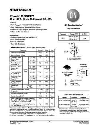
NTMFS4834N Power MOSFET 30 V, 130 A, Single N-Channel, SO-8FL Features Low RDS(on) to Minimize Conduction Losses Low Capacitance to Minimize Driver Losses http //onsemi.com Optimized Gate Charge to Minimize Switching Losses These are Pb-Free Devices V(BR)DSS RDS(ON) MAX ID MAX Applications 3.0 mW @ 10 V Refer to Application Note AND8195/D 30 V 130 A 4.0 mW @ 4
ntmfs4925n-d.pdf
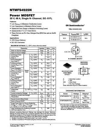
NTMFS4925N Power MOSFET 30 V, 48 A, Single N-Channel, SO-8 FL Features Low RDS(on) to Minimize Conduction Losses Low Capacitance to Minimize Driver Losses Optimized Gate Charge to Minimize Switching Losses http //onsemi.com Optimized for 5 V, 12 V Gate Drives These Devices are Pb-Free, Halogen Free/BFR Free and are RoHS V(BR)DSS RDS(ON) MAX ID MAX Compliant 6.0 m
ntmfs4846n.pdf

NTMFS4846N Power MOSFET 30 V, 100 A, Single N-Channel, SO-8FL Features Low RDS(on) to Minimize Conduction Losses Low Capacitance to Minimize Driver Losses Optimized Gate Charge to Minimize Switching Losses http //onsemi.com Thermally Enhanced SO8 Package These are Pb-Free Devices* V(BR)DSS RDS(ON) MAX ID MAX Applications 3.4 mW @ 10 V Refer to Application No
ntmfs5c410nlt.pdf
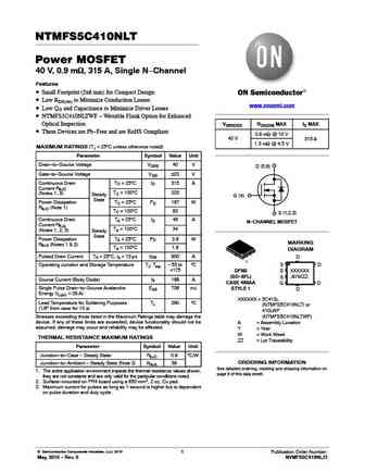
NTMFS5C410NLT Power MOSFET 40 V, 0.9 mW, 315 A, Single N-Channel Features Small Footprint (5x6 mm) for Compact Design Low RDS(on) to Minimize Conduction Losses www.onsemi.com Low QG and Capacitance to Minimize Driver Losses NTMFS5C410NLTWF - Wettable Flank Option for Enhanced Optical Inspection V(BR)DSS RDS(ON) MAX ID MAX These Devices are Pb-Free and are RoHS Com
ntmfs4701nt1g.pdf
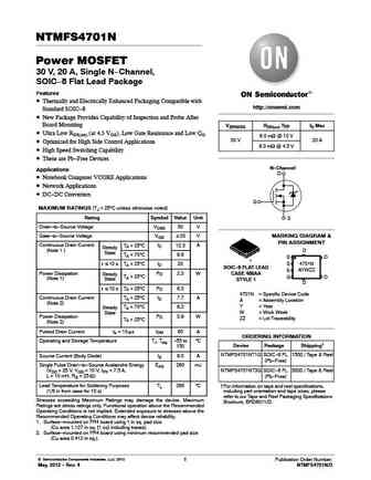
NTMFS4701N Power MOSFET 30 V, 20 A, Single N-Channel, SOIC-8 Flat Lead Package Features Thermally and Electrically Enhanced Packaging Compatible with http //onsemi.com Standard SOIC-8 New Package Provides Capability of Inspection and Probe After Board Mounting V(BR)DSS RDS(on) Typ ID Max Ultra Low RDS(on) (at 4.5 VGS), Low Gate Resistance and Low QG 6.0 mW @ 10 V 30 V
ntmfs4120nt1g.pdf
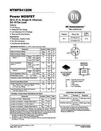
NTMFS4120N Power MOSFET 30 V, 31 A, Single N-Channel, SO-8 Flat Lead Features Low RDS(on) http //onsemi.com Optimized Gate Charge Low Inductance SO-8 Package ID Max V(BR)DSS RDS(on) Typ These are Pb-Free Devices (Note 1) Applications 3.5 mW @ 10 V 30 V 31 A Notebooks, Graphics Cards 4.2 mW @ 4.5 V DC-DC Converters Synchronous Rectification D MAXI
ntmfs4c59n.pdf
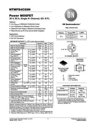
NTMFS4C59N Power MOSFET 30 V, 52 A, Single N-Channel, SO-8 FL Features Low RDS(on) to Minimize Conduction Losses Low Capacitance to Minimize Driver Losses http //onsemi.com Optimized Gate Charge to Minimize Switching Losses These Devices are Pb-Free and are RoHS Compliant V(BR)DSS RDS(ON) MAX ID MAX Applications 5.8 mW @ 10 V CPU Power Delivery 30 V 52 A 8.5 mW
ntmfs4c290n.pdf
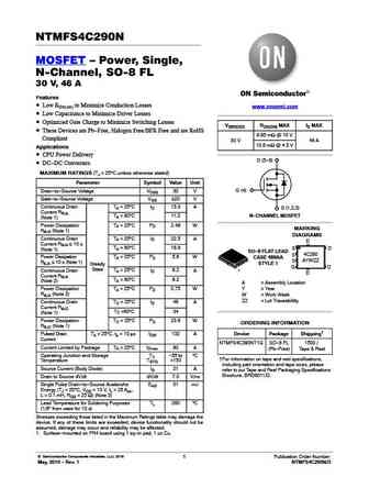
NTMFS4C290N MOSFET Power, Single, N-Channel, SO-8 FL 30 V, 46 A Features Low RDS(on) to Minimize Conduction Losses www.onsemi.com Low Capacitance to Minimize Driver Losses Optimized Gate Charge to Minimize Switching Losses V(BR)DSS RDS(ON) MAX ID MAX These Devices are Pb-Free, Halogen Free/BFR Free and are RoHS 6.95 mW @ 10 V Compliant 30 V 46 A 10.8 mW @ 4.5 V
ntmfs4707n.pdf
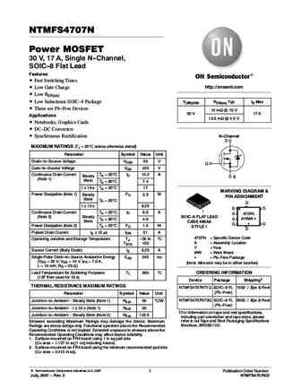
NTMFS4707N Power MOSFET 30 V, 17 A, Single N-Channel, SOIC-8 Flat Lead Features Fast Switching Times http //onsemi.com Low Gate Charge Low RDS(on) Low Inductance SOIC-8 Package V(BR)DSS RDS(on) Typ ID Max These are Pb-Free Devices 10 mW @ 10 V 30 V 17 A Applications 13.5 mW @ 4.5 V Notebooks, Graphics Cards DC-DC Converters Synchronous Rectific
ntmfs4h013nf.pdf
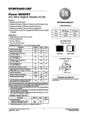
NTMFS4H013NF Power MOSFET 25 V, 269 A, Single N-Channel, SO-8FL Features Integrated Schottky Diode Optimized Design to Minimize Conduction and Switching Losses www.onsemi.com Optimized Package to Minimize Parasitic Inductances Optimized material for improved thermal performance These Devices are Pb-Free, Halogen Free/BFR Free and are RoHS VGS MAX RDS(on) TYP QGTOT
ntmfs4923net1g.pdf
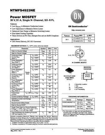
NTMFS4923NE Power MOSFET 30 V, 91 A, Single N-Channel, SO-8 FL Features Low RDS(on) to Minimize Conduction Losses Low Capacitance to Minimize Driver Losses http //onsemi.com Optimized Gate Charge to Minimize Switching Losses Dual Sided Cooling Capability V(BR)DSS RDS(ON) MAX ID MAX These Devices are Pb-Free, Halogen Free and are RoHS Compliant 3.3 mW @ 10 V 91 A
ntmfs4899nft1g.pdf
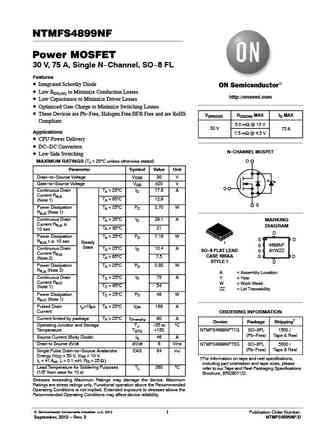
NTMFS4899NF Power MOSFET 30 V, 75 A, Single N-Channel, SO-8 FL Features Integrated Schottky Diode Low RDS(on) to Minimize Conduction Losses http //onsemi.com Low Capacitance to Minimize Driver Losses Optimized Gate Charge to Minimize Switching Losses These Devices are Pb-Free, Halogen Free/BFR Free and are RoHS V(BR)DSS RDS(ON) MAX ID MAX Compliant 5.0 mW @ 10 V
Другие MOSFET... NTMFD5C674NLT1G , NTMFD6H840NLT1G , NTMFD6H846NLT1G , NTMFS006N12MCT1G , NTMFS008N12MCT1G , NTMFS015N10MCLT1G , NTMFS0D8N02P1ET1G , NTMFS0D9N03CGT1G , AO3407 , NTMFS1D7N03CGT1G , NTMFS23D9N06HLT1G , NTMFS3D6N10MCLT1G , NTMFS4C05NT1G , NTMFS4D2N10MDT1G , NTMFS5C404NLTT1G , NTMFS5C404NT3G , NTMFS5C406NLT1G .
History: P0465CI
History: P0465CI
🌐 : EN ES РУ

Список транзисторов
Обновления
MOSFET: AUN084N10 | AUN065N10 | AUN063N10 | AUN062N08BG | AUN060N08AG | AUN053N10 | AUN050N08BGL | AUN045N085 | AUN042N055 | AUN036N10 | AUD069N10A | AUD062N08BG | AUD060N08AG | AUD060N055 | AUD056N08BGL | AUB062N08BG
Popular searches
2sa606 | 2n3644 | 2sc2240bl | 2sc1913 | c2314 transistor | c2482 transistor | 2sc1222 replacement | 2sa725