WM02DN70M3. Аналоги и основные параметры
Наименование производителя: WM02DN70M3
Тип транзистора: MOSFET
Полярность: N
Предельные значения
Pd ⓘ - Максимальная рассеиваемая мощность: 1.5 W
|Vds|ⓘ - Максимально допустимое напряжение сток-исток: 20 V
|Vgs|ⓘ - Максимально допустимое напряжение затвор-исток: 12 V
|Id| ⓘ - Максимально допустимый постоянный ток стока: 7 A
Tj ⓘ - Максимальная температура канала: 150 °C
Электрические характеристики
tr ⓘ - Время нарастания: 10.5 ns
Cossⓘ - Выходная емкость: 130 pf
RDSonⓘ - Сопротивление сток-исток открытого транзистора: 0.017 Ohm
Тип корпуса: SOT23-6L
Аналог (замена) для WM02DN70M3
- подборⓘ MOSFET транзистора по параметрам
WM02DN70M3 даташит
wm02dn70m3.pdf
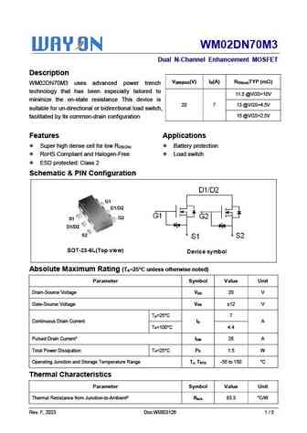
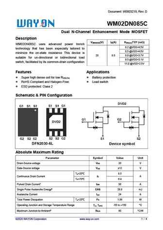
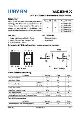
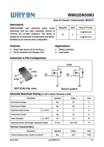
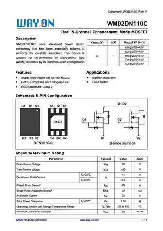
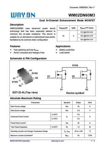
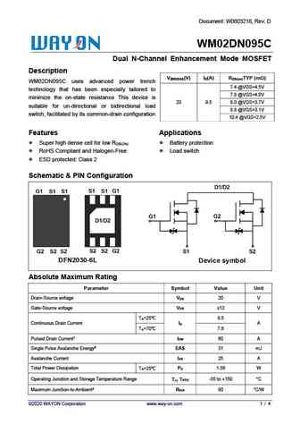
WM02DN70M3 Dual N-Channel Enhancement MOSFET Description V (V) I (A) R TYP (m ) (BR)DSS D DS(on) WM02DN70M3 uses advanced power trench technology that has been especially tailored to 11.5 @VGS=10V minimize the on-state resistance This device is 20 7 13 @VGS=4.5V suitable for un-directional or bidirectional load switch, 15 @VGS=2.5V facilitated by its common-drain config
wm02dn70a.pdf
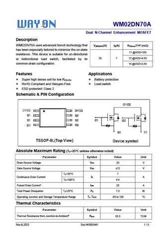
WM02DN70A Dual N-Channel Enhancement MOSFET Description WM02DN70A uses advanced trench technology that V (V) I (A) R TYP (m ) (BR)DSS D DS(on) has been especially tailored to minimize the on-state 11 @VGS=10V resistance. This device is suitable for un-directional 20 7 12 @VGS=4.5V or bidirectional load switch, facilitated by its common-drain configuration. 15 @VGS=2.5V
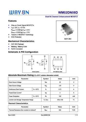
wm02dn08t.pdf
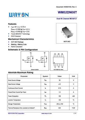
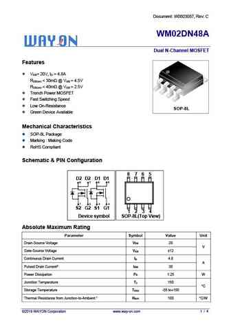
Document W0803109, Rev C WM02DN08T T Dual N-Channel MOSFET Features V = 20 V, I = 0.75 A DS D R
wm02dn560q.pdf
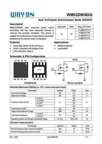
WM02DN560Q Dual N-Channel Enhancement Mode MOSFET Description V (V) I (A) R TYP (m ) (BR)DSS D DS(on) WM02DN560Q uses advanced power trench 4.2 @VGS=4.5V technology that has been especially tailored to 4.3 @VGS=3.9V minimize the on-state resistance This device is 20 56 4.7 @VGS=3.1V suitable for un-directional or bidirectional load switch, 5.0 @VGS=2.5V facilitated
Другие MOSFET... WM02DN08T , WM02DN095C , WM02DN110C , WM02DN48A , WM02DN50M3 , WM02DN560Q , WM02DN60M3 , WM02DN70A , IRF3710 , WM02DP06D , WM02N08F , WM02N08FB , WM02N08G , WM02N08H , WM02N08L , WM02N20F , WM02N20G .
History: WMK28N65F2 | WMM15N80M3 | CS55N25A8R-G | WMO05N80M3 | WML9N90D1B | WMM08N70EM
History: WMK28N65F2 | WMM15N80M3 | CS55N25A8R-G | WMO05N80M3 | WML9N90D1B | WMM08N70EM
🌐 : EN ES РУ

Список транзисторов
Обновления
MOSFET: AUB034N10 | AUB033N08BG | AUB026N085 | AUA062N08BG | AUA060N08AG | AUA056N08BGL | AUA039N10 | ASW80R290E | ASW65R120EFD | ASW65R110E | ASW65R095EFD | ASW65R046EFD | ASW65R041EFDA | ASW65R041E | ASW60R150E | ASW60R090EFDA
Popular searches
irfb438 | mj21193g | irf3710 pinout | irf9530 datasheet | mj21194 | oc71 transistor | 2n3440 | bc550c