FDS8928A datasheet, аналоги, основные параметры
Наименование производителя: FDS8928A 📄📄
Тип транзистора: MOSFET
Полярность: NP
Предельные значения
Pd ⓘ - Максимальная рассеиваемая мощность: 2 W
|Vds|ⓘ - Максимально допустимое напряжение сток-исток: 30 V
|Vgs|ⓘ - Максимально допустимое напряжение затвор-исток: 8 V
|Id| ⓘ - Максимально допустимый постоянный ток стока: 5.5 A
Tj ⓘ - Максимальная температура канала: 150 °C
Электрические характеристики
tr ⓘ - Время нарастания: 19 ns
Cossⓘ - Выходная емкость: 410 pf
RDSonⓘ - Сопротивление сток-исток открытого транзистора: 0.03 Ohm
Тип корпуса: SO-8
📄📄 Копировать
Аналог (замена) для FDS8928A
- подборⓘ MOSFET транзистора по параметрам
FDS8928A даташит
..1. Size:153K fairchild semi
fds8928a.pdf 
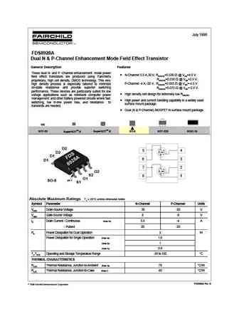
July 1998 FDS8928A Dual N & P-Channel Enhancement Mode Field Effect Transistor General Description Features These dual N- and P -Channel enhancement mode power N-Channel 5.5 A,30 V, RDS(ON)=0.030 @ VGS=4.5 V field effect transistors are produced using Fairchild's RDS(ON)=0.038 @ VGS=2.5 V. proprietary, high cell density, DMOS technology. This very P-Channel -4 A,-20 V, RDS(
..2. Size:265K onsemi
fds8928a.pdf 
Is Now Part of To learn more about ON Semiconductor, please visit our website at www.onsemi.com Please note As part of the Fairchild Semiconductor integration, some of the Fairchild orderable part numbers will need to change in order to meet ON Semiconductor s system requirements. Since the ON Semiconductor product management systems do not have the ability to manage part nomenclatur
8.1. Size:69K fairchild semi
fds8926a.pdf 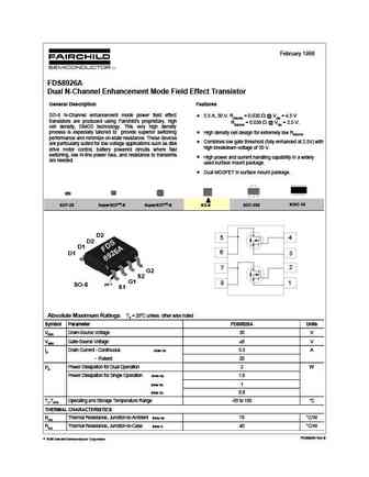
February 1998 FDS8926A Dual N-Channel Enhancement Mode Field Effect Transistor General Description Features SO-8 N-Channel enhancement mode power field effect 5.5 A, 30 V. RDS(ON) = 0.030 @ VGS = 4.5 V transistors are produced using Fairchild's proprietary, high RDS(ON) = 0.038 @ VGS = 2.5 V. cell density, DMOS technology. This very high density process is especially tailore
9.1. Size:521K fairchild semi
fds8958a.pdf 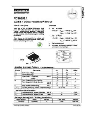
April 2008 tm FDS8958A Dual N & P-Channel PowerTrench MOSFET General Description Features These dual N- and P-Channel enhancement mode Q1 N-Channel power field effect transistors are produced using 7.0A, 30V RDS(on) = 0.028 @ VGS = 10V Fairchild Semiconductor s advanced PowerTrench process that has been especially tailored to minimize RDS(on) = 0.
9.2. Size:285K fairchild semi
fds8934a.pdf 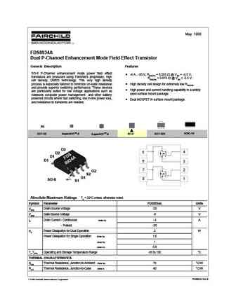
May 1998 FDS8934A Dual P-Channel Enhancement Mode Field Effect Transistor General Description Features SO-8 P-Channel enhancement mode power field effect -4 A , -20 V, RDS(ON) = 0.055 @ VGS = -4.5 V, transistors are produced using Fairchild's proprietary, high RDS(ON) = 0.072 @ VGS = -2.5 V. cell density, DMOS technology. This very high density process is especially tailor
9.3. Size:798K fairchild semi
fds8958a f085.pdf 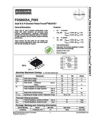
February 2010 tm FDS8958A_F085 Dual N & P-Channel PowerTrench MOSFET General Description Features These dual N- and P-Channel enhancement mode Q1 N-Channel power field effect transistors are produced using 7.0A, 30V RDS(on) = 0.028 @ VGS = 10V Fairchild Semiconductor s advanced PowerTrench process that has been especially tailored to minimize RDS(on
9.4. Size:539K fairchild semi
fds8949 f085.pdf 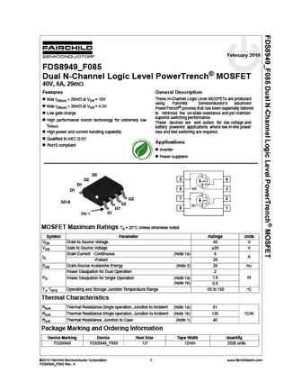
February 2010 FDS8949_F085 tm Dual N-Channel Logic Level PowerTrench MOSFET 40V, 6A, 29m Features General Description These N-Channel Logic Level MOSFETs are produced Max rDS(on) = 29m at VGS = 10V using Fairchild Semiconductor s advanced Max rDS(on) = 36m at VGS = 4.5V PowerTrench process that has been especially tailored Low gate charge to minimize the on-state
9.5. Size:384K fairchild semi
fds8984.pdf 
May 2007 FDS8984 tm N-Channel PowerTrench MOSFET 30V, 7A, 23m General Description Features Max rDS(on) = 23m , VGS = 10V, ID = 7A This N-Channel MOSFET has been designed specifically to improve the overall efficiency of DC/DC converters using Max rDS(on) = 30m , VGS = 4.5V, ID = 6A either synchronous or conventional switching PWM controllers. It has been optimized for
9.6. Size:219K fairchild semi
fds8935.pdf 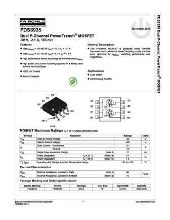
November 2010 FDS8935 Dual P-Channel PowerTrench MOSFET -80 V, -2.1 A, 183 m Features General Description Max rDS(on) = 183 m at VGS = -10 V, ID = -2.1 A This P-channel MOSFET is produced using Fairchild Semiconductor s advanced PowerTrench process that has Max rDS(on) = 247 m at VGS = -4.5 V, ID = -1.9 A been optimized for rDS(on), switching performance and ruggedn
9.7. Size:1203K fairchild semi
fds8958b.pdf 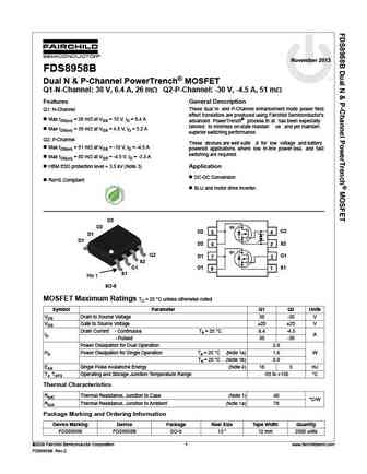
November 2013 FDS8958B Dual N & P-Channel PowerTrench MOSFET Q1-N-Channel 30 V, 6.4 A, 26 m Q2-P-Channel -30 V, -4.5 A, 51 m Features General Description These dual N- and P-Channel enhancement mode power field Q1 N-Channel effect transistors are produced using Fairchild Semiconductor's Max rDS(on) = 26 m at VGS = 10 V, ID = 6.4 A advanced PowerTrench process th at
9.8. Size:159K fairchild semi
fds8960c.pdf 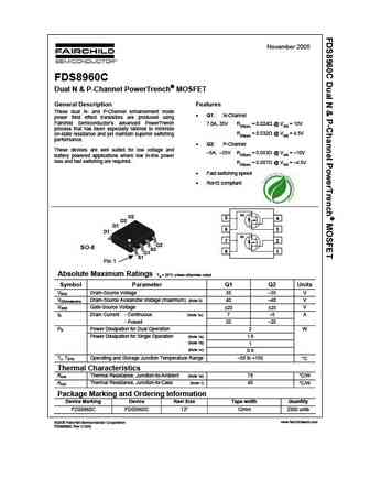
November 2005 FDS8960C Dual N & P-Channel PowerTrench MOSFET General Description Features These dual N- and P-Channel enhancement mode Q1 N-Channel power field effect transistors are produced using Fairchild Semiconductor s advanced PowerTrench 7.0A, 35V RDS(on) = 0.024 @ VGS = 10V process that has been especially tailored to minimize RDS(on) = 0.032 @ VGS = 4.
9.9. Size:277K fairchild semi
fds89161lz.pdf 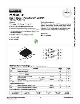
June 2011 FDS89161LZ Dual N-Channel PowerTrench MOSFET 100 V, 2.7 A, 105 m Features General Description Max rDS(on) = 105 m at VGS = 10 V, ID = 2.7 A This N-Channel logic Level MOSFETs are produced using Fairchild Semiconductor s advanced Power Trench process Max rDS(on) = 160 m at VGS = 4.5 V, ID = 2.1 A that has been special tailored to minimize the on-state High
9.10. Size:345K fairchild semi
fds8949.pdf 
October 2006 FDS8949 tm Dual N-Channel Logic Level PowerTrench MOSFET 40V, 6A, 29m Features General Description These N-Channel Logic Level MOSFETs are produced Max rDS(on) = 29m at VGS = 10V using Fairchild Semiconductor s advanced Max rDS(on) = 36m at VGS = 4.5V PowerTrench process that has been especially tailored Low gate charge to minimize the on-state resist
9.11. Size:693K fairchild semi
fds8978.pdf 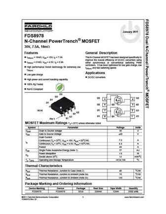
January 2011 FDS8978 N-Channel PowerTrench MOSFET 30V, 7.5A, 18m Features General Description rDS(on) = 18m , VGS = 10V, ID = 7.5A This N-Channel MOSFET has been designed specifically to improve the overall efficiency of DC/DC converters using rDS(on) = 21m , VGS = 4.5V, ID = 6.9A either synchronous or conventional switching PWM controllers. It has been optimized for low
9.12. Size:440K fairchild semi
fds8984 f085.pdf 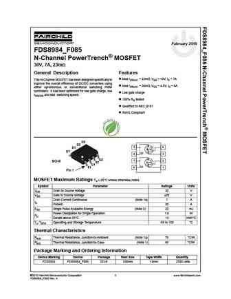
Fabruary 2010 FDS8984_F085 tm N-Channel PowerTrench MOSFET 30V, 7A, 23m General Description Features Max rDS(on) = 23m , VGS = 10V, ID = 7A This N-Channel MOSFET has been designed specifically to improve the overall efficiency of DC/DC converters using Max rDS(on) = 30m , VGS = 4.5V, ID = 6A either synchronous or conventional switching PWM controllers. It has been opti
9.13. Size:674K fairchild semi
fds8962c.pdf 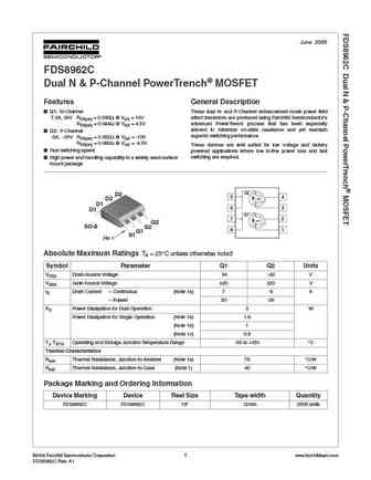
June 2006 FDS8962C Dual N & P-Channel PowerTrench MOSFET Features General Description Q1 N-Channel These dual N- and P-Channel enhancement mode power field 7.0A, 30V RDS(on) = 0.030 @ VGS = 10V effect transistors are produced using Fairchild Semiconductor s RDS(on) = 0.044 @ VGS = 4.5V advanced PowerTrench process that has been especially tailored to minimize on-state re
9.14. Size:260K fairchild semi
fds89161.pdf 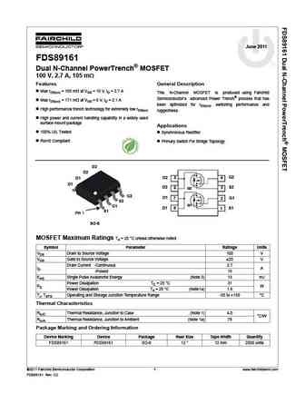
June 2011 FDS89161 Dual N-Channel PowerTrench MOSFET 100 V, 2.7 A, 105 m Features General Description Max rDS(on) = 105 m at VGS = 10 V, ID = 2.7 A This N-Channel MOSFET is produced using Fairchild Semiconductor s advanced Power Trench process that has Max rDS(on) = 171 m at VGS = 6 V, ID = 2.1 A been optimized for rDS(on), switching performance and High performance
9.15. Size:240K fairchild semi
fds89141.pdf 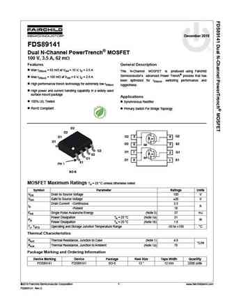
December 2010 FDS89141 Dual N-Channel PowerTrench MOSFET 100 V, 3.5 A, 62 m Features General Description Max rDS(on) = 62 m at VGS = 10 V, ID = 3.5 A This N-Channel MOSFET is produced using Fairchild Semiconductor s advanced Power Trench process that has Max rDS(on) = 100 m at VGS = 6 V, ID = 2.8 A been optimized for rDS(on), switching performance and High performan
9.16. Size:423K onsemi
fds8984-f085.pdf 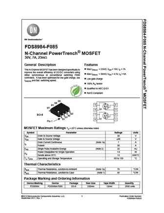
FDS8984-F085 N-Channel PowerTrench MOSFET 30V, 7A, 23m General Description Features Max rDS(on) = 23m , VGS = 10V, ID = 7A This N-Channel MOSFET has been designed specifically to improve the overall efficiency of DC/DC converters using Max rDS(on) = 30m , VGS = 4.5V, ID = 6A either synchronous or conventional switching PWM controllers. It has been optimized for low gate c
9.17. Size:454K onsemi
fds8949-f085.pdf 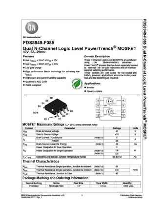
FDS8949-F085 Dual N-Channel Logic Level PowerTrench MOSFET 40V, 6A, 29m Features General Description These N-Channel Logic Level MOSFETs are produced Max rDS(on) = 29m at VGS = 10V using ON Semiconductor s advanced Max rDS(on) = 36m at VGS = 4.5V PowerTrench process that has been especially tailored Low gate charge to minimize the on-state resistance and yet mainta
9.18. Size:537K onsemi
fds8958a-f085.pdf 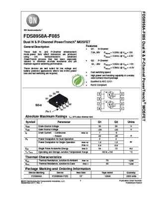
FDS8958A-F085 Dual N & P-Channel PowerTrench MOSFET Features General Description Q1 N-Channel These dual N- and P-Channel enhancement 7.0A, 30V RDS(on) = 0.028 @ VGS = 10V mode power field effect transistors are produced RDS(on) = 0.040 @ VGS = 4.5V using ON Semiconductor s advanced PowerTrench process that has been especially Q2 P-Channel tailored to m
9.19. Size:384K onsemi
fds8984.pdf 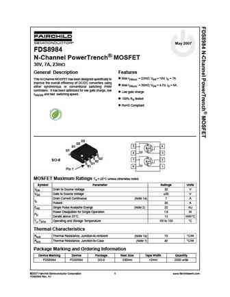
May 2007 FDS8984 tm N-Channel PowerTrench MOSFET 30V, 7A, 23m General Description Features Max rDS(on) = 23m , VGS = 10V, ID = 7A This N-Channel MOSFET has been designed specifically to improve the overall efficiency of DC/DC converters using Max rDS(on) = 30m , VGS = 4.5V, ID = 6A either synchronous or conventional switching PWM controllers. It has been optimized for
9.20. Size:253K onsemi
fds8935.pdf 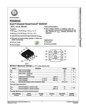
FDS8935 Dual P-Channel PowerTrench MOSFET -80 V, -2.1 A, 183 m General Description This P-channel MOSFET is produced using ON Features Semiconductor s advanced PowerTrench process that has Max rDS(on) = 183 m at VGS = -10 V, ID = -2.1 A been optimized for rDS(on), switching performance and ruggedness. Max rDS(on) = 247 m at VGS = -4.5 V, ID = -1.9 A High performanc
9.21. Size:635K onsemi
fds8958b.pdf 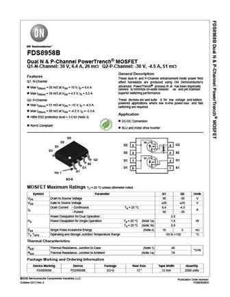
FDS8958B Dual N & P-Channel PowerTrench MOSFET Q1-N-Channel 30 V, 6.4 A, 26 m Q2-P-Channel -30 V, -4.5 A, 51 m General Description Features These dual N- and P-Channel enhancement mode power field Q1 N-Channel effect transistors are produced using ON Semiconductor's advanced PowerTrench process th at has been especially Max rDS(on) = 26 m at VGS = 10 V, ID = 6.4 A
9.22. Size:394K onsemi
fds89161lz.pdf 
Is Now Part of To learn more about ON Semiconductor, please visit our website at www.onsemi.com Please note As part of the Fairchild Semiconductor integration, some of the Fairchild orderable part numbers will need to change in order to meet ON Semiconductor s system requirements. Since the ON Semiconductor product management systems do not have the ability to manage part nomenclatur
9.23. Size:345K onsemi
fds8949.pdf 
October 2006 FDS8949 tm Dual N-Channel Logic Level PowerTrench MOSFET 40V, 6A, 29m Features General Description These N-Channel Logic Level MOSFETs are produced Max rDS(on) = 29m at VGS = 10V using Fairchild Semiconductor s advanced Max rDS(on) = 36m at VGS = 4.5V PowerTrench process that has been especially tailored Low gate charge to minimize the on-state resist
9.24. Size:393K onsemi
fds89161.pdf 
Is Now Part of To learn more about ON Semiconductor, please visit our website at www.onsemi.com Please note As part of the Fairchild Semiconductor integration, some of the Fairchild orderable part numbers will need to change in order to meet ON Semiconductor s system requirements. Since the ON Semiconductor product management systems do not have the ability to manage part nomenclatur
9.25. Size:373K onsemi
fds89141.pdf 
Is Now Part of To learn more about ON Semiconductor, please visit our website at www.onsemi.com Please note As part of the Fairchild Semiconductor integration, some of the Fairchild orderable part numbers will need to change in order to meet ON Semiconductor s system requirements. Since the ON Semiconductor product management systems do not have the ability to manage part nomenclatur
9.26. Size:2683K kexin
fds89161.pdf 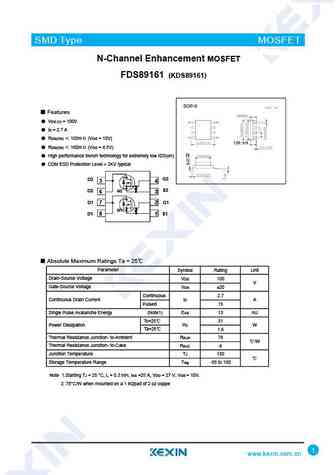
SMD Type MOSFET N-Channel Enhancement MOSFET FDS89161 (KDS89161) SOP-8 Features VDS (V) = 100V ID = 2.7 A RDS(ON) 105m (VGS = 10V) 1.50 0.15 RDS(ON) 160m (VGS = 4.5V) High performance trench technology for extremely low rDS(on) CDM ESD Protection Level > 2KV typical G2 D2 5 4 D2 S2 Q2 6 3 D1 G1 7 2 Q1 D1 8 1 S1 atings Ta = 25
9.27. Size:1492K cn vbsemi
fds8960c.pdf 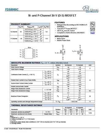
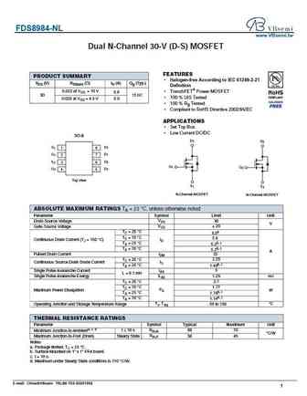
FDS8960C www.VBsemi.tw N- and P-Channel 30 V (D-S) MOSFET FEATURES PRODUCT SUMMARY Halogen-free According to IEC 61249-2-21 VDS (V) RDS(on) ( ) Definition ID (A)a Qg (Typ.) TrenchFET Power MOSFET 0.018 at VGS = 10 V 8e 100 % Rg and UIS Tested N-Channel 30 0.020 at VGS = 8 V 8e 6.2 Compliant to RoHS Directive 2002/95/EC 0.024 at VGS = 4.5 V 8e 0.032 at VGS
9.29. Size:1560K cn vbsemi
fds8949.pdf 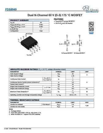
FDS8949 www.VBsemi.tw Dual N-Channel 60 V (D-S) 175 C MOSFET FEATURES PRODUCT SUMMARY TrenchFET power MOSFET VDS (V) 60 100 % Rg and UIS tested RDS(on) ( ) at VGS = 10 V 0.040 RDS(on) ( ) at VGS = 4.5 V 0.055 ID (A) per leg 7 Configuration Dual SO-8 Dual D2 D1 D2 D2 5 D1 6 D1 7 8 G1 G2 4 G2 3 3 S1 S2 S2 S2 2 2 G G1 1 1 N-Channel MOSFET N-Channel
Другие IGBT... FDS8896, SP2458, FDS89141, SP2112, FDS89161, SP2110, FDS89161LZ, SP2108, SKD502T, SP2107, SP2106, FDS8935, FDS8949, FDS8949F085, FDS8958AF085, SP2103, SP2102