MP10N50EI datasheet, аналоги, основные параметры
Наименование производителя: MP10N50EI
Тип транзистора: MOSFET
Полярность: N
Предельные значения
Pd ⓘ
- Максимальная рассеиваемая мощность: 32 W
|Vds|ⓘ - Максимально допустимое напряжение сток-исток: 500 V
|Vgs|ⓘ - Максимально допустимое напряжение затвор-исток: 30 V
|Id| ⓘ - Максимально допустимый постоянный ток стока: 10 A
Tj ⓘ - Максимальная температура канала: 150 °C
Электрические характеристики
tr ⓘ -
Время нарастания: 46.4 ns
Cossⓘ - Выходная емкость: 148 pf
RDSonⓘ - Сопротивление сток-исток открытого транзистора: 0.7 Ohm
Тип корпуса: TO220F
Аналог (замена) для MP10N50EI
- подборⓘ MOSFET транзистора по параметрам
MP10N50EI даташит
..1. Size:567K jilin sino
mp10n50ei.pdf 
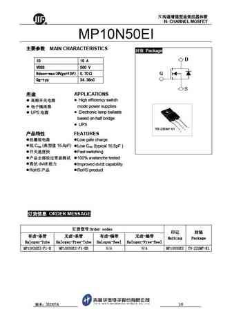
N N- CHANNEL MOSFET R MP10N50EI MAIN CHARACTERISTICS Package ID 10 A VDSS 500 V Rdson-max @Vgs=10V 0.70 Qg-typ 34.38nC APPLICATIONS High efficiency switch mode power supplies - Electronic lamp ballasts UPS based on half bridge
9.1. Size:555K fuji
fmp10n60e.pdf 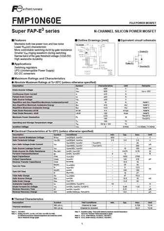
FMP10N60E FUJI POWER MOSFET Super FAP-E3 series N-CHANNEL SILICON POWER MOSFET Features Outline Drawings [mm] Equivalent circuit schematic Maintains both low power loss and low noise TO-220AB Lower R (on) characteristic DS More controllable switching dv/dt by gate resistance Drain(D) Smaller V ringing waveform during switching GS Narrow band of the gate threshold voltage (3.0 0.5V)
9.2. Size:1199K jilin sino
mp10n60eif mp10n60eib mp10n60eis mp10n60eic.pdf 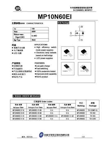
N R N-CHANNEL MOSFET MP10N60EI Package MAIN CHARACTERISTICS ID 10A VDSS 600V Rdson-max 0.66 Vgs=10V Qg-Typ 35nC APPLICATIONS High efficiency switch mode power supplies Electronic lamp ballasts LED based on half bridge LE
9.3. Size:609K trinnotech
tmp10n80 tmpf10n80.pdf 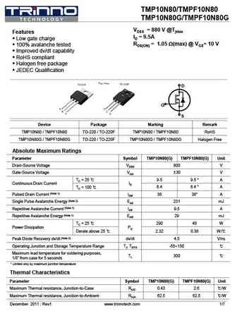
TMP10N80/TMPF10N80 TMP10N80G/TMPF10N80G VDSS = 880 V @Tjmax Features ID = 9.5A Low gate charge RDS(ON) = 1.05 W(max) @ VGS= 10 V 100% avalanche tested Improved dv/dt capability RoHS compliant Halogen free package JEDEC Qualification D G S Device Package Marking Remark TMP10N80 / TMPF10N80 TO-220 / TO-220F TMP10N80 / TMPF10N80 RoHS TMP10N
9.4. Size:609K trinnotech
tmp10n60a tmpf10n60a.pdf 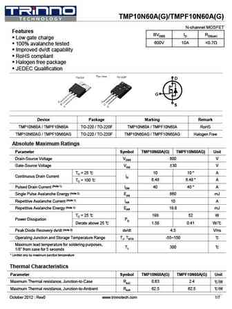
TMP10N60A(G)/TMPF10N60A(G) N-channel MOSFET Features BVDSS ID RDS(on) Low gate charge 600V 10A
9.5. Size:335K trinnotech
tmp10n60 tmpf10n60.pdf 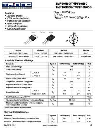
TMP10N60/TMPF10N60 TMP10N60G/TMPF10N60G VDSS = 660 V @Tjmax Features ID = 10A Low gate charge RDS(on) = 0.75 W(max) @ VGS= 10 V 100% avalanche tested Improved dv/dt capability RoHS compliant Halogen free package JEDEC Qualification D G S Device Package Marking Remark TMP10N60 / TMPF10N60 TO-220 / TO-220F TMP10N60 / TMPF10N60 RoHS TMP10N60G / TMPF10N60G
9.6. Size:577K trinnotech
tmp10n65 tmpf10n65.pdf 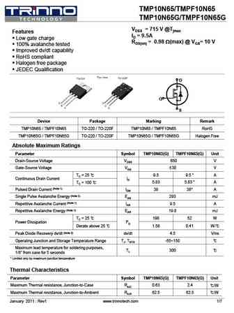
TMP10N65/TMPF10N65 TMP10N65G/TMPF10N65G VDSS = 715 V @Tjmax Features ID = 9.5A Low gate charge RDS(on) = 0.98 W(max) @ VGS= 10 V 100% avalanche tested Improved dv/dt capability RoHS compliant Halogen free package JEDEC Qualification D G S Device Package Marking Remark TMP10N65 / TMPF10N65 TO-220 / TO-220F TMP10N65 / TMPF10N65 RoHS TMP10N
9.7. Size:607K trinnotech
tmp10n65a tmpf10n65a.pdf 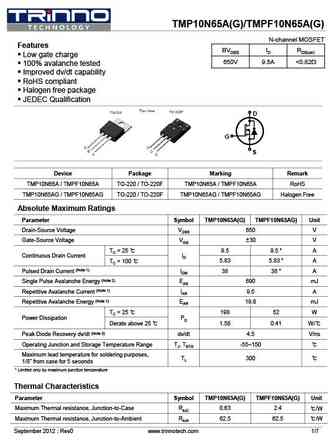
TMP10N65A(G)/TMPF10N65A(G) N-channel MOSFET Features BVDSS ID RDS(on) Low gate charge 650V 9.5A
9.8. Size:671K way-on
wmm10n65c4 wml10n65c4 wmo10n65c4 wmn10n65c4 wmp10n65c4 wmk10n65c4.pdf 
WMM10N65C4, WML10N6 WM C4 65C4, MO10N65C WMN10N65C4, WMP10N6 WM C4 65C4, MK10N65C 650V 0.52 S T V Super Junction Power MOSFET Descrip ption WMOSTM C4 is Wa 4th generation super ayon s n junction MOSFET fa that is utilizing charge M amily S balance te or extremely esistance echnology fo y low on-re D S D G G G S D G and low ga charge performanc WMOSTM
9.9. Size:677K way-on
wml10n100c2 wmn10n100c2 wmm10n100c2 wmj10n100c2 wmo10n100c2 wmp10n100c2 wmk10n100c2.pdf 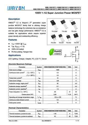
WM 2, WMN10N MM10N100C ML10N100C2 N100C2, WM C2 WMJ10N100C2, WM C2, WMP10N MK10N100C MO10N100C N100C2, WM C2 1000V 1.1 S T 0 Super Junction Power MOSFET Descrip ption WMOSTM C2 is Wa 2nd generation super ayon s n junction MOSFET fa that is utilizing charge M amily S balance te or extremely esistance D echnology fo y low on-re S S G D D G G G and low ga
9.10. Size:678K way-on
wml10n105c2 wmn10n105c2 wmm10n105c2 wmj10n105c2 wmo10n105c2 wmp10n105c2 wmk10n105c2.pdf 
WM 2, WMN10N MM10N105C ML10N105C2 N105C2, WM C2 WMJ10N105C2, WM C2, WMP10N MK10N105C MO10N105C N105C2, WM C2 1050V 1.1 S T 0 Super Junction Power MOSFET Descrip ption WMOSTM C2 is Wa 2nd generation super ayon s n junction MOSFET fa that is utilizing charge M amily S balance te or extremely esistance D echnology fo y low on-re S S G D D G G G and low ga
9.11. Size:659K way-on
wml10n65em wmk10n65em wmm10n65em wmn10n65em wmp10n65em wmo10n65em.pdf 
WML10 WMK10N6 0N65EM, W 65EM, WMM10N65EM WMN10 WMP10N6 0N65EM, W 65EM, WMO10N65EM 650V 0.52 S T V Super Junction Power MOSFET Descrip ption WMOSTM EM is Wayon s 3rd generation super W n junction MOSFET fa that is utilizing charge M amily S balance te or extremely esistance echnology fo y low on-re S D D G G G S D G T and low ga ce. WMOSTM EM is ate
9.12. Size:668K way-on
wmm10n70c4 wml10n70c4 wmo10n70c4 wmn10n70c4 wmp10n70c4 wmk10n70c4.pdf 
WMM10N70C4, WML10N7 WM C4 70C4, MO10N70C WMN10N70C4, WMP10N7 WM C4 70C4, MK10N70C 700V 0.52 S T V Super Junction Power MOSFET Descrip ption WMOSTM C4 is Wa 4th generation super ayon s n junction MOSFET fa that is utilizing charge M amily S balance te or extremely esistance echnology fo y low on-re D S D G G G S D G and low ga charge performanc WMOSTM
9.13. Size:660K way-on
wml10n70em wmk10n70em wmm10n70em wmn10n70em wmp10n70em wmo10n70em.pdf 
WML10 WMK10N7 0N70EM, W 70EM, WMM10N70EM WMN10 WMP10N7 0N70EM, W 70EM, WMO10N70EM 700V 0.52 S T V Super Junction Power MOSFET Descrip ption WMOSTM EM is Wayon s 3rd generation super W n junction MOSFET fa that is utilizing charge M amily S balance te or extremely esistance echnology fo y low on-re S D D G G G S D G T and low ga ce. WMOSTM EM is ate
9.14. Size:670K way-on
wmm10n60c4 wml10n60c4 wmo10n60c4 wmn10n60c4 wmp10n60c4 wmk10n60c4.pdf 
WMM10N60C4, WML10N6 WM C4 60C4, MO10N60C WMN10N60C4, WMP10N6 WM C4 60C4, MK10N60C 600V 0.52 S T V Super Junction Power MOSFET Descrip ption WMOSTM C4 is Wa 4th generation super ayon s n junction MOSFET fa that is utilizing charge M amily S balance te or extremely esistance echnology fo y low on-re D S D G G G S D G and low ga charge performanc WMOSTM
9.15. Size:675K way-on
wml10n80m3 wmn10n80m3 wmm10n80m3 wmo10n80m3 wmp10n80m3 wmk10n80m3.pdf 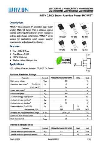
WML10N80M3, W 80M3, WM M3 WMN10N8 MM10N80M WMO1 80M3, WM M3 10N80M3, WMP10N8 MK10N80M 800V 0.86 S T V Super Junction Power MOSFET Descrip ption WMOSTM M3 is Wayo neration 800 M on s 3rd gen 0V super junction MOSFET fa that is utilizing charge M amily S balance te or extremely esistance D echnology fo y low on-re S S G D D G G G T and low ga charge perfo
9.16. Size:340K cn wuxi unigroup
tma10n65h tmp10n65h.pdf 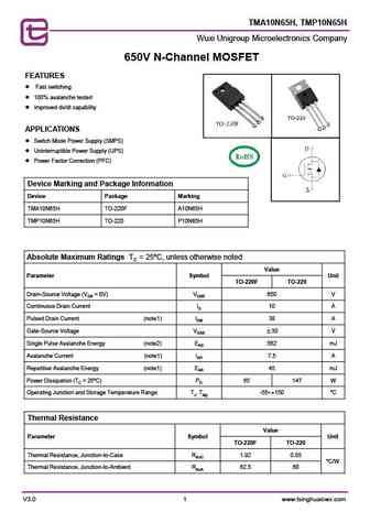
TMA10N65H, TMP10N65H Wuxi Unigroup Microelectronics Company 650V N-Channel MOSFET FEATURES Fast switching 100% avalanche tested Improved dv/dt capability APPLICATIONS Switch Mode Power Supply (SMPS) Uninterruptible Power Supply (UPS) Power Factor Correction (PFC) Device Marking and Package Information Device Package Marking TMA10N65H TO-220F A1
Другие IGBT... MC10N006, MC10N007L, MC10N020, MC10N020AL, MC11N005, MG065R060, MG120R040, MG120R080, K3569, MP10N60EIB, MP10N60EIC, MP10N60EIF, MP10N60EIS, MP15N60EIB, MP15N60EIC, MP15N60EIF, MP15N60EIS
