NCEP0230D datasheet, аналоги, основные параметры
Наименование производителя: NCEP0230D
Тип транзистора: MOSFET
Полярность: N
Предельные значения
Pd ⓘ
- Максимальная рассеиваемая мощность: 135 W
|Vds|ⓘ - Максимально допустимое напряжение сток-исток: 200 V
|Vgs|ⓘ - Максимально допустимое напряжение затвор-исток: 20 V
|Id| ⓘ - Максимально допустимый постоянный ток стока: 30 A
Tj ⓘ - Максимальная температура канала: 175 °C
Электрические характеристики
tr ⓘ -
Время нарастания: 9 ns
Cossⓘ - Выходная емкость: 128 pf
RDSonⓘ - Сопротивление сток-исток открытого транзистора: 0.045 Ohm
Тип корпуса: TO-263
Аналог (замена) для NCEP0230D
- подборⓘ MOSFET транзистора по параметрам
NCEP0230D даташит
..1. Size:691K ncepower
ncep0230d.pdf 
Pb Free Product http //www.ncepower.com NCEP0230D NCE N-Channel Super Trench II Power MOSFET Description General Features The NCEP0230D uses Super Trench II technology that is V =200V,I =30A DS D uniquely optimized to provide the most efficient high R =40m (typical) @ V =10V DS(ON) GS frequency switching performance. Both conduction and Excellent gate charge x R product(FO
7.1. Size:797K ncepower
ncep023nh85agu.pdf 
NCEP023NH85AGU http //www.ncepower.com NCE N-Channel Super Trench III Power MOSFET (Primary) Description General Features The NCEP023NH85AGU uses Super Trench III technology V =85V,I =250A DS D that is uniquely optimized to provide the most efficient high R =1.9m (typical) @ V =10V DS(ON) GS frequency switching performance. Both conduction and R =2.6m (typical) @ V =4.5V DS(ON)
7.2. Size:855K ncepower
ncep023n10d.pdf 
NCEP023N10, NCEP023N10D NCE N-Channel Super Trench II Power MOSFET Description The series of devices uses Super Trench II technology that is General Features uniquely optimized to provide the most efficient high frequency V =100V,I =240A DS D switching performance. Both conduction and switching power R =2.1m , typical (TO-220)@ V =10V DS(ON) GS losses are minimized due to an ext
7.3. Size:2030K ncepower
ncep023n10t.pdf 
NCEP023N10T NCE N-Channel Super Trench II Power MOSFET Description The series of devices uses Super Trench II technology that is General Features uniquely optimized to provide the most efficient high frequency V =100V,I =280A DS D switching performance. Both conduction and switching power R =1.85m , typical@ V =10V DS(ON) GS losses are minimized due to an extremely low combinati
7.4. Size:687K ncepower
ncep023nh85gu.pdf 
NCEP023NH85GU http //www.ncepower.com NCE N-Channel Super Trench III Power MOSFET Description General Features The NCEP023NH85GU uses Super Trench III technology that V =85V,I =245A DS D is uniquely optimized to provide the most efficient high R =2.1m (typical) @ V =10V DS(ON) GS frequency switching performance. Both conduction and Excellent gate charge x R product(FOM) D
7.5. Size:635K ncepower
ncep023n10 ncep023n10d.pdf 
NCEP023N10, NCEP023N10D NCE N-Channel Super Trench II Power MOSFET Description The series of devices uses Super Trench II technology that is General Features uniquely optimized to provide the most efficient high frequency VDS =100V,ID =240A switching performance. Both conduction and switching power RDS(ON)=2.0m , typical (TO-220)@ VGS=10V losses are minimized due to an ext
7.6. Size:939K ncepower
ncep023n85m.pdf 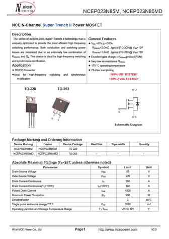
NCEP023N85M, NCEP023N85MD NCE N-Channel Super Trench II Power MOSFET Description The series of devices uses Super Trench II technology that is General Features uniquely optimized to provide the most efficient high frequency V =85V,I =260A DS D switching performance. Both conduction and switching power R =2.0m , typical (TO-220)@ V =10V DS(ON) GS losses are minimized due to an ex
7.7. Size:940K ncepower
ncep023n85.pdf 
NCEP023N85, NCEP023N85D NCE N-Channel Super Trench II Power MOSFET Description The series of devices uses Super Trench II technology that is General Features uniquely optimized to provide the most efficient high frequency V =85V,I =260A DS D switching performance. Both conduction and switching power R =2.0m , typical (TO-220)@ V =10V DS(ON) GS losses are minimized due to an extr
7.8. Size:940K ncepower
ncep023n85d.pdf 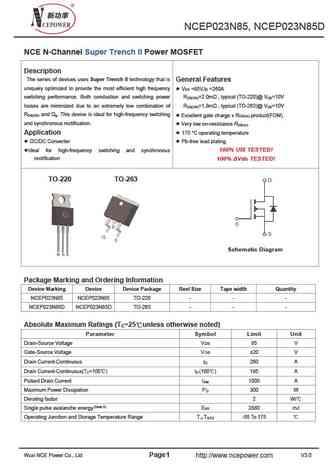
NCEP023N85, NCEP023N85D NCE N-Channel Super Trench II Power MOSFET Description The series of devices uses Super Trench II technology that is General Features uniquely optimized to provide the most efficient high frequency V =85V,I =260A DS D switching performance. Both conduction and switching power R =2.0m , typical (TO-220)@ V =10V DS(ON) GS losses are minimized due to an extr
7.9. Size:412K ncepower
ncep023n85 ncep023n85d.pdf 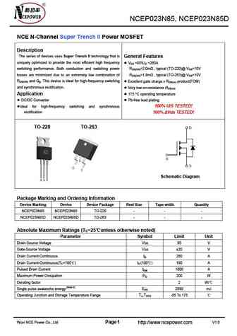
NCEP023N85, NCEP023N85D NCE N-Channel Super Trench II Power MOSFET Description The series of devices uses Super Trench II technology that is General Features uniquely optimized to provide the most efficient high frequency VDS =85V,ID =260A switching performance. Both conduction and switching power RDS(ON)=2.0m , typical (TO-220)@ VGS=10V losses are minimized due to an ext
7.10. Size:409K ncepower
ncep023n10ll.pdf 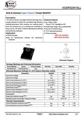
NCEP023N10LL NCE N-Channel Super Trench II Power MOSFET Description The series of devices uses Super Trench II technology that is General Features uniquely optimized to provide the most efficient high frequency VDS =100V,ID =300A switching performance. Both conduction and switching power RDS(ON)=1.7m , typical@ VGS=10V losses are minimized due to an extremely low combinat
7.11. Size:400K ncepower
ncep023n85t.pdf 
NCEP023N85T NCE N-Channel Super Trench II Power MOSFET Description General Features The series of devices uses Super Trench II technology that is VDS =85V,ID =290A uniquely optimized to provide the most efficient high frequency RDS(ON)=1.8m , typical@ VGS=10V switching performance. Both conduction and switching power Excellent gate charge x RDS(on) product(FOM) lo
7.12. Size:855K ncepower
ncep023n10.pdf 
NCEP023N10, NCEP023N10D NCE N-Channel Super Trench II Power MOSFET Description The series of devices uses Super Trench II technology that is General Features uniquely optimized to provide the most efficient high frequency V =100V,I =240A DS D switching performance. Both conduction and switching power R =2.1m , typical (TO-220)@ V =10V DS(ON) GS losses are minimized due to an ext
7.13. Size:713K ncepower
ncep023nh30gu.pdf 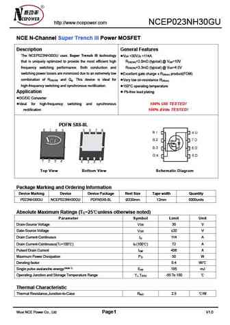
http //www.ncepower.com NCEP023NH30GU NCE N-Channel Super Trench III Power MOSFET Description General Features The NCEP023NH30GU uses Super Trench III technology V =30V,I =114A DS D that is uniquely optimized to provide the most efficient high R =2.0m (typical) @ V =10V DS(ON) GS frequency switching performance. Both conduction and R =3.3m (typical) @ V =4.5V DS(ON) GS switchi
Другие IGBT... NCEP0210Q, NCEP0212F, NCEP0218G, NCEP0218K, NCEP0220F, NCEP0225F, NCEP0225G, NCEP0225K, AO4407A, NCEP023N10T, NCEP023N85M, NCEP023N85T, NCEP023NH30GU, NCEP02503S, NCEP02505S, NCEP02515F, NCEP02525G
