NCEP072N10A datasheet, аналоги, основные параметры
Наименование производителя: NCEP072N10A
Тип транзистора: MOSFET
Полярность: N
Предельные значения
Pd ⓘ
- Максимальная рассеиваемая мощность: 125 W
|Vds|ⓘ - Максимально допустимое напряжение сток-исток: 100 V
|Vgs|ⓘ - Максимально допустимое напряжение затвор-исток: 20 V
|Id| ⓘ - Максимально допустимый постоянный ток стока: 88 A
Tj ⓘ - Максимальная температура канала: 175 °C
Электрические характеристики
tr ⓘ -
Время нарастания: 11 ns
Cossⓘ - Выходная емкость: 322 pf
RDSonⓘ - Сопротивление сток-исток открытого транзистора: 0.0096 Ohm
Тип корпуса: TO-220
Аналог (замена) для NCEP072N10A
- подборⓘ MOSFET транзистора по параметрам
NCEP072N10A даташит
..1. Size:627K ncepower
ncep072n10a.pdf 
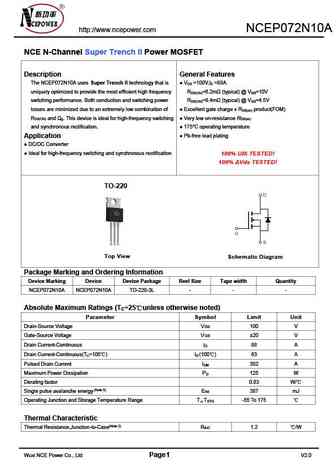
http //www.ncepower.com NCEP072N10A NCE N-Channel Super Trench II Power MOSFET Description General Features The NCEP072N10A uses Super Trench II technology that is V =100V,I =88A DS D uniquely optimized to provide the most efficient high frequency R =6.2m (typical) @ V =10V DS(ON) GS switching performance. Both conduction and switching power R =8.4m (typical) @ V =4.5V DS(ON) GS
4.1. Size:305K ncepower
ncep072n10.pdf 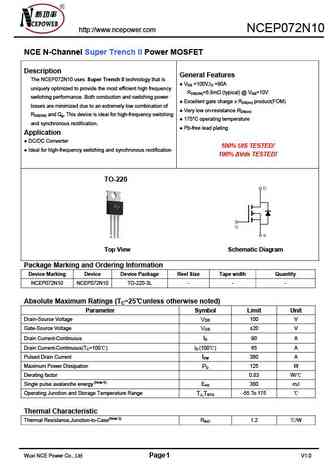
http //www.ncepower.com NCEP072N10 NCE N-Channel Super Trench II Power MOSFET Description General Features The NCEP072N10 uses Super Trench II technology that is VDS =100V,ID =90A uniquely optimized to provide the most efficient high frequency RDS(ON)=6.8m (typical) @ VGS=10V switching performance. Both conduction and switching power Excellent gate charge x RDS(on) p
8.1. Size:331K ncepower
ncep075n85agu.pdf 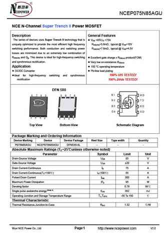
NCEP075N85AGU NCE N-Channel Super Trench II Power MOSFET Description General Features The series of devices uses Super Trench II technology that is VDS =85V,ID =75A uniquely optimized to provide the most efficient high frequency RDS(ON)=5.6m , typical @ VGS=10V switching performance. Both conduction and switching power RDS(ON)=7.6m , typical @ VGS=4.5V losses are minimiz
8.2. Size:760K ncepower
ncep075n85gu.pdf 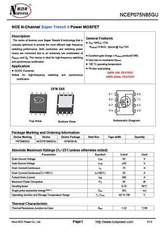
NCEP075N85GU NCE N-Channel Super Trench II Power MOSFET Description General Features The series of devices uses Super Trench II technology that is V =85V,I =75A DS D uniquely optimized to provide the most efficient high frequency R =5.6m , typical @ V =10V DS(ON) GS switching performance. Both conduction and switching power losses are minimized due to an extremely low combinati
8.3. Size:397K ncepower
ncep070n10agu.pdf 
NCEP070N10AGU NCE N-Channel Super Trench II Power MOSFET Description General Features The series of devices uses Super Trench II technology that is VDS =100V,ID =80A uniquely optimized to provide the most efficient high frequency RDS(ON)=6.1m , typical@ VGS=10V switching performance. Both conduction and switching power RDS(ON)=8.35m , typical@ VGS=4.5V losses are minimiz
8.4. Size:335K ncepower
ncep070n12.pdf 
NCEP070N12,NCEP070N12D NCE N-Channel Super Trench II Power MOSFET Description General Features The series of devices uses Super Trench II technology that is VDS =120V,ID =100A uniquely optimized to provide the most efficient high frequency RDS(ON)=6.5m , typical (TO-220)@ VGS=10V switching performance. Both conduction and switching power RDS(ON)=6.3m , typical (TO-26
8.5. Size:335K ncepower
ncep070n12 ncep070n12d.pdf 
NCEP070N12,NCEP070N12D NCE N-Channel Super Trench II Power MOSFET Description General Features The series of devices uses Super Trench II technology that is VDS =120V,ID =100A uniquely optimized to provide the most efficient high frequency RDS(ON)=6.5m , typical (TO-220)@ VGS=10V switching performance. Both conduction and switching power RDS(ON)=6.3m , typical (TO-26
8.6. Size:335K ncepower
ncep070n12d.pdf 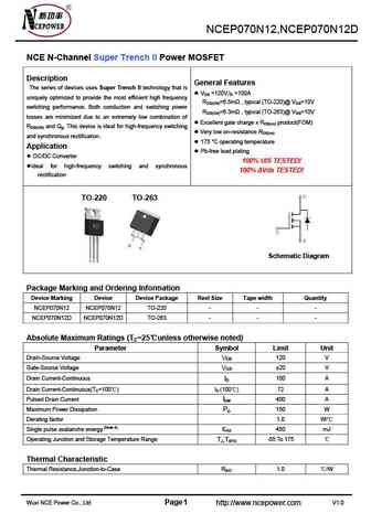
NCEP070N12,NCEP070N12D NCE N-Channel Super Trench II Power MOSFET Description General Features The series of devices uses Super Trench II technology that is VDS =120V,ID =100A uniquely optimized to provide the most efficient high frequency RDS(ON)=6.5m , typical (TO-220)@ VGS=10V switching performance. Both conduction and switching power RDS(ON)=6.3m , typical (TO-26
8.7. Size:462K ncepower
ncep078n10ak.pdf 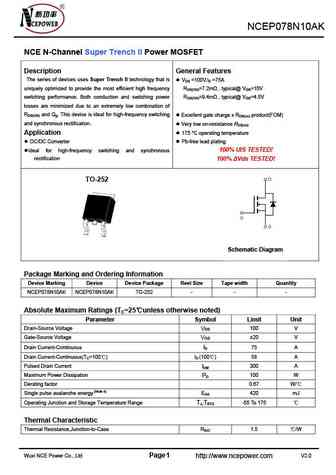
NCEP078N10AK NCE N-Channel Super Trench II Power MOSFET Description General Features The series of devices uses Super Trench II technology that is VDS =100V,ID =75A uniquely optimized to provide the most efficient high frequency RDS(ON)=7.2m , typical@ VGS=10V switching performance. Both conduction and switching power RDS(ON)=9.4m , typical@ VGS=4.5V losses are minimized
8.8. Size:377K ncepower
ncep070n10gu.pdf 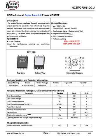
NCEP070N10GU NCE N-Channel Super Trench II Power MOSFET Description The series of devices uses Super Trench II technology that is General Features uniquely optimized to provide the most efficient high frequency VDS =100V,ID =80A switching performance. Both conduction and switching power RDS(ON)=6.6m , typical@ VGS=10V losses are minimized due to an extremely low combinati
8.9. Size:428K ncepower
ncep078n10ag.pdf 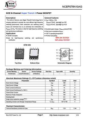
NCEP078N10AG NCE N-Channel Super Trench II Power MOSFET Description General Features The series of devices uses Super Trench II technology that is VDS =100V,ID =75A uniquely optimized to provide the most efficient high frequency RDS(ON)=7.0m , typical@ VGS=10V switching performance. Both conduction and switching power RDS(ON)=9.2m , typical@ VGS=4.5V losses are minimized
8.10. Size:1009K ncepower
ncep078n10g.pdf 
NCEP078N10G NCE N-Channel Super Trench II Power MOSFET Description The series of devices uses Super Trench II technology that is General Features uniquely optimized to provide the most efficient high frequency V =100V,I =75A DS D switching performance. Both conduction and switching power R =7.4m , typical@ V =10V DS(ON) GS losses are minimized due to an extremely low combination
Другие IGBT... NCEP065N10GU, NCEP065N12AGU, NCEP065N85D, NCEP068N10K, NCEP070N10AGU, NCEP070N10GU, NCEP070N12, NCEP070N12D, AON7408, NCEP075N85AGU, NCEP075N85GU, NCEP078N10AG, NCEP078N10AK, NCEP078N10G, NCEP080N10, NCEP080N10A, NCEP080N10F
