D5N65-XAD. Аналоги и основные параметры
Наименование производителя: D5N65-XAD
Тип транзистора: MOSFET
Полярность: N
Предельные значения
Pd ⓘ
- Максимальная рассеиваемая мощность: 75 W
|Vds|ⓘ - Максимально допустимое напряжение сток-исток: 650 V
|Vgs|ⓘ - Максимально допустимое напряжение затвор-исток: 30 V
|Id| ⓘ - Максимально допустимый постоянный ток стока: 5 A
Tj ⓘ - Максимальная температура канала: 150 °C
Электрические характеристики
tr ⓘ -
Время нарастания: 8.8 ns
Cossⓘ - Выходная емкость: 55 pf
RDSonⓘ - Сопротивление сток-исток открытого транзистора: 2.4 Ohm
Тип корпуса: TO252
Аналог (замена) для D5N65-XAD
- подборⓘ MOSFET транзистора по параметрам
D5N65-XAD даташит
..1. Size:1238K cn wxdh
d5n65-xad.pdf 
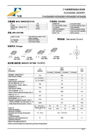
D5N65-XAD 5A 650V N-channel Enhancement Mode Power MOSFET 1 Description These N-channel enhanced vdmosfets, is obtained by the self-aligned V DSS = 650V planar technology which reduce the conduction loss, improve switching I = 5.0A D performance and enhance the avalanche energy. Which accords with the RoHS standard. TO-220F provides insulation voltage rated at 2000V R DS(on) TYP)
9.1. Size:836K 1
swd5n65k.pdf 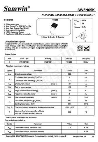
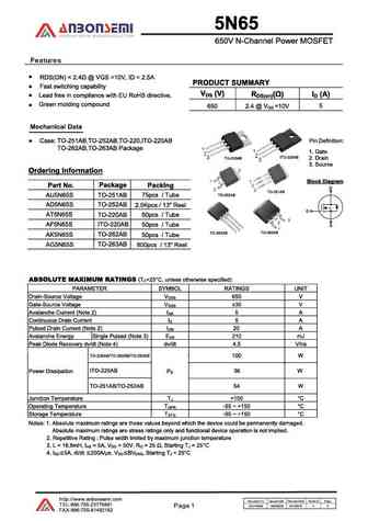
SW5N65K N-channel Enhanced mode TO-252 MOSFET Features TO-252 BVDSS 650V ID 5A High ruggedness Low RDS(ON) (Typ 0.8 )@VGS=10V RDS(ON) 0.8 Low Gate Charge (Typ 10.3nC) Improved dv/dt Capability 2 100% Avalanche Tested 1 2 Application LED, Charge, Adaptor 3 1. Gate 2. Drain 3. Source 1 3 General Description This power MOSFE
9.2. Size:688K blue-rocket-elect
brd5n65.pdf 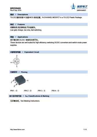
BRD5N65 Rev.A Sep.-2016 DATA SHEET / Descriptions TO-252 N MOS N-CHANNEL MOSFET in a TO-252 Plastic Package. / Features , , Low gate charge, low crss, fast switching. / Applications DC/DC These devices are well suited for high efficiency
9.3. Size:255K winsemi
wfd5n65l.pdf 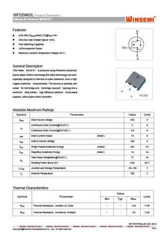
WFD5N65L Product Description Silicon N-Channel MOSFET Silicon N-Channel MOSFET Silicon N-Channel MOSFET Silicon N-Channel MOSFET Features D 5.0A,650V,R (Max2.7 )@V =10V DS(on) GS Ultra-low Gate charge(Typical 12nC) Fast Switching Capability G 100%Avalanche Tested Maximum Junction Temperature Range(150 ) S General Description This Power MOSFET is produced
9.6. Size:463K maple semi
sld5n65s slu5n65s.pdf 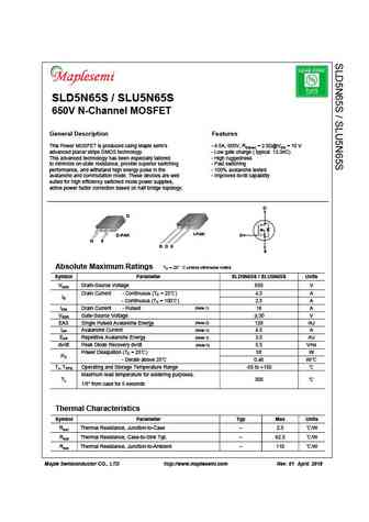
SLD5N65S / SLU5N65S SLD5N65S / SLU5N65S 650V N-Channel MOSFET General Description Features This Power MOSFET is produced using Maple semi s - 4.5A, 650V, RDS(on) = 2.5 @VGS = 10 V advanced planar stripe DMOS technology. - Low gate charge ( typical 13.3nC) This advanced technology has been especially tailored - High ruggedness to minimize on-state resistance, provide superior switching
9.7. Size:667K samwin
swd5n65k.pdf 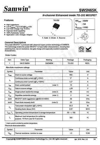
SW5N65K N-channel Enhanced mode TO-252 MOSFET Features TO-252 BVDSS 650V ID 5A High ruggedness Low RDS(ON) (Typ 0.8 )@VGS=10V RDS(ON) 0.8 Low Gate Charge (Typ 10.3nC) Improved dv/dt Capability 2 100% Avalanche Tested 1 2 Application LED, Charger, Adaptor 3 1. Gate 2. Drain 3. Source 1 3 General Description This power MOSF
9.8. Size:209K semihow
hfd5n65u.pdf 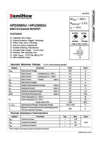
Jan 2014 BVDSS = 650 V RDS(on) typ = 2.3 HFD5N65U / HFU5N65U ID = 3.6 A 650V N-Channel MOSFET D-PAK I-PAK FEATURES 2 1 Originative New Design 1 3 2 3 Superior Avalanche Rugged Technology HFD5N65U HFU5N65U Robust Gate Oxide Technology 1.Gate 2. Drain 3. Source Very Low Intrinsic Capacitances Excellent Switching Characteristics Unrivalled Gate Charge 10.5 nC
9.9. Size:1121K semihow
hfu5n65sa hfd5n65sa.pdf 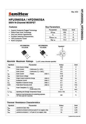
May. 2022 HFU5N65SA / HFD5N65SA 650V N-Channel MOSFET Features Key Parameters Parameter Value Unit Superior Avalanche Rugged Technology BVDSS 650 V Robust Gate Oxide Technology Very Low Intrinsic Capacitances ID 4.2 A Excellent Switching Characteristics RDS(on), Typ 2.3 100% Avalanche Tested Qg, Typ 14.2 nC RoHS Compliant HFU5N65SA HFD5N65SA Symbol TO
9.10. Size:204K semihow
hfd5n65s.pdf 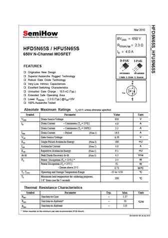
Mar 2010 BVDSS = 650 V RDS(on) typ = 2.3 HFD5N65S / HFU5N65S ID = 4.0 A 650V N-Channel MOSFET D-PAK I-PAK 2 2 FEATURES 1 1 3 2 3 Originative New Design HFD5N65S HFU5N65S Superior Avalanche Rugged Technology 1.Gate 2. Drain 3. Source Robust Gate Oxide Technology Very Low Intrinsic Capacitances Excellent Switching Characteristics Unrivalled Gate Charge 10.5 nC (Typ
9.11. Size:1206K truesemi
tsd5n65m tsu5n65m.pdf 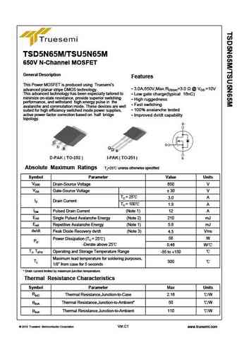
TSD5N65M/TSU5N65M 650V N-Channel MOSFET General Description Features This Power MOSFET is produced using Truesemi s 3.0A,650V,Max.RDS(on)=3.0 @ VGS =10V advanced planar stripe DMOS technology. This advanced technology has been especially tailored to Low gate charge(typical 16nC) minimize on-state resistance, provide superior switching High ruggedness performance, and
9.13. Size:1292K lonten
lnc5n65b lnd5n65b lng5n65b lnh5n65b.pdf 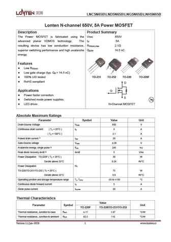
LNC5N65B LND5N65B LNG5N65B LNH5N65B Lonten N-channel 650V, 5A Power MOSFET Description Product Summary The Power MOSFET is fabricated using the V 650V DSS advanced planar VDMOS technology. The I 5A D resulting device has low conduction resistance, R 2.1 DS(on),max superior switching performance and high avalanche Q 14.5 nC g,typ energy. Features Low R DS(on) Low gate ch
9.14. Size:1380K cn vgsemi
hckd5n65bm2.pdf 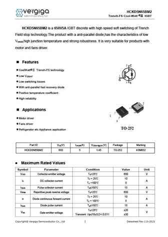
HCKD5N65BM2 @ Trench-FS Cool-Watt IGBT HCKD5N65BM2 is a 650V5A IGBT discrete with high speed soft switching of Trench Field stop technology.The product with a anti-parallel diode,has the characteristics of low V ,high junction temperature and strong robustness. It is very suitable for products with cesat motor and fans driver. Features CoolWatt@ Trench-FS technology
9.15. Size:1381K cn vgsemi
hckd5n65am2.pdf 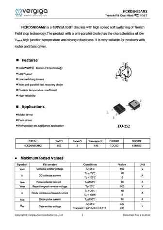
HCKD5N65AM2 @ Trench-FS Cool-Watt IGBT HCKD5N65AM2 is a 650V5A IGBT discrete with high speed soft switching of Trench Field stop technology.The product with a anti-parallel diode,has the characteristics of low V ,high junction temperature and strong robustness. It is very suitable for products with cesat motor and fans driver. Features CoolWatt@ Trench-FS technology
9.16. Size:262K inchange semiconductor
wfd5n65l.pdf 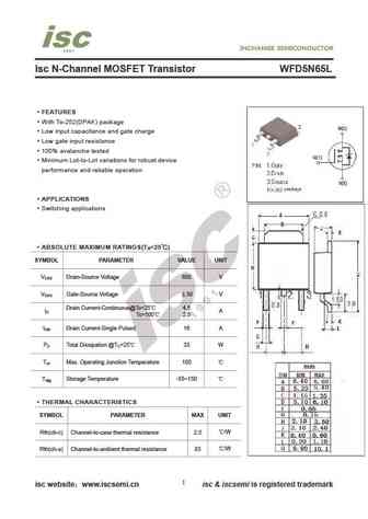
Isc N-Channel MOSFET Transistor WFD5N65L FEATURES With To-252(DPAK) package Low input capacitance and gate charge Low gate input resistance 100% avalanche tested Minimum Lot-to-Lot variations for robust device performance and reliable operation APPLICATIONS Switching applications ABSOLUTE MAXIMUM RATINGS(T =25 ) a SYMBOL PARAMETER VALUE UNIT V Drain-Source Volta
Другие MOSFET... DH009N02F
, DH009N02I
, DH009N02P
, DH012N03
, DH012N03B
, D12N06
, D18N20
, D25N10
, IRFB4115
, D630
, D640
, D740
, D7N60
, D7N70
, D80N06
, D8N50
, D9N65
.