F18N50 datasheet, аналоги, основные параметры
Наименование производителя: F18N50 📄📄
Тип транзистора: MOSFET
Полярность: N
Предельные значения
Pd ⓘ - Максимальная рассеиваемая мощность: 43 W
|Vds|ⓘ - Максимально допустимое напряжение сток-исток: 500 V
|Vgs|ⓘ - Максимально допустимое напряжение затвор-исток: 30 V
|Id| ⓘ - Максимально допустимый постоянный ток стока: 18 A
Tj ⓘ - Максимальная температура канала: 150 °C
Электрические характеристики
tr ⓘ - Время нарастания: 65 ns
Cossⓘ - Выходная емкость: 277 pf
RDSonⓘ - Сопротивление сток-исток открытого транзистора: 0.35 Ohm
Тип корпуса: TO220F
📄📄 Копировать
Аналог (замена) для F18N50
- подборⓘ MOSFET транзистора по параметрам
F18N50 даташит
..1. Size:1413K cn wxdh
f18n50.pdf 
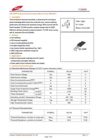
F18N50 18A 500V N-channel Enhancement Mode Power MOSFET 1 Description These N-channel enhanced vdmosfets, is obtained by the self-aligned V DSS = 500V planar technology which reduce the conduction loss, improve switching I = 18.0A D performance and enhance the avalanche energy. Which accords with the RoHS standard. TO-220F provides insulation voltage rated at 2000V R DS(on) TYP)
0.1. Size:1208K 1
fqp18n50v2 fqpf18n50v2.pdf 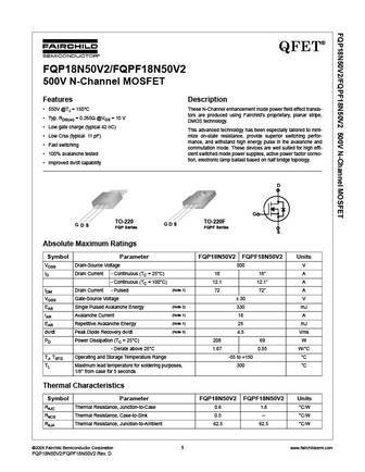
QFET FQP18N50V2/FQPF18N50V2 500V N-Channel MOSFET Features Description 550V @TJ = 150 C These N-Channel enhancement mode power field effect transis- tors are produced using Fairchild s proprietary, planar stripe, Typ. RDS(on) = 0.265 @VGS = 10 V DMOS technology. Low gate charge (typical 42 nC) This advanced technology has been especially tailored to mini- Lo
0.2. Size:870K fairchild semi
fdp18n50 fdpf18n50 fdpf18n50t.pdf 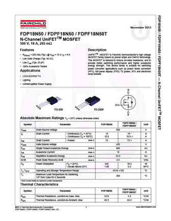
November 2013 FDP18N50 / FDPF18N50 / FDPF18N50T N-Channel UniFETTM MOSFET 500 V, 18 A, 265 m Features Description RDS(on) = 220 m (Typ.) @ VGS = 10 V, ID = 9 A UniFETTM MOSFET is Fairchild Semiconductor s high voltage MOSFET family based on planar stripe and DMOS technology. Low Gate Charge (Typ. 45 nC) This MOSFET is tailored to reduce on-state resistance, and to Low
0.3. Size:466K fairchild semi
fdp18n50 fdpf18n50.pdf 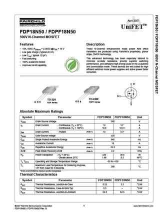
April 2007 TM UniFET FDP18N50 / FDPF18N50 500V N-Channel MOSFET Features Description 18A, 500V, RDS(on) = 0.265 @VGS = 10 V These N-Channel enhancement mode power field effect transistors are produced using Fairchild s proprietary, planar Low gate charge ( typical 45 nC) stripe, DMOS technology. Low Crss ( typical 25 pF) This advanced technology has been especially
0.4. Size:844K fairchild semi
fqpf18n50v2.pdf 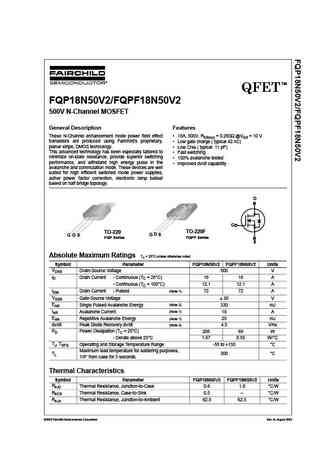
TM QFET FQP18N50V2/FQPF18N50V2 500V N-Channel MOSFET General Description Features These N-Channel enhancement mode power field effect 18A, 500V, RDS(on) = 0.265 @VGS = 10 V transistors are produced using Fairchild s proprietary, Low gate charge ( typical 42 nC) planar stripe, DMOS technology. Low Crss ( typical 11 pF) This advanced technology has been especially tailor
0.5. Size:168K vishay
sihf18n50c.pdf 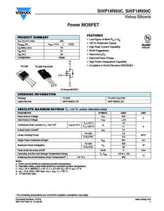
SiHP18N50C, SiHF18N50C Vishay Siliconix Power MOSFET FEATURES PRODUCT SUMMARY Low Figure-of-Merit Ron x Qg VDS (V) at TJ max. 560 100 % Avalanche Tested RDS(on) ( )VGS = 10 V 0.225 High Peak Current Capability Qg (Max.) (nC) 76 dV/dt Ruggedness Qgs (nC) 21 Qgd (nC) 29 Improved trr/Qrr Configuration Single Improved Gate Charge D High Power Dissipati
0.6. Size:169K vishay
sihf18n50d.pdf 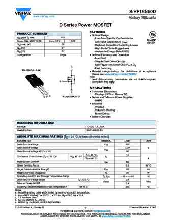
SiHF18N50D www.vishay.com Vishay Siliconix D Series Power MOSFET FEATURES PRODUCT SUMMARY Optimal Design VDS (V) at TJ max. 550 - Low Area Specific On-Resistance RDS(on) max. at 25 C ( ) VGS = 10 V 0.28 - Low Input Capacitance (Ciss) Qg (max.) (nC) 76 - Reduced Capacitive Switching Losses Qgs (nC) 11 - High Body Diode Ruggedness Qgd (nC) 17 - Avalanche Energy Rated (UIS)
0.7. Size:238K ixys
ixz4df18n50.pdf 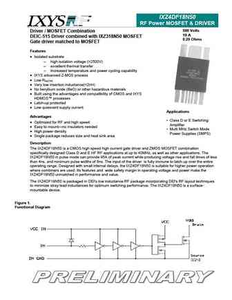
IXZ4DF18N50 RF Power MOSFET & DRIVER 500 Volts Driver / MOSFET Combination 19 A DEIC-515 Driver combined with IXZ318N50 MOSFET 0.29 Ohms Gate driver matched to MOSFET Features Isolated substrate - high isolation voltage (>2500V) - excellent thermal transfer - Increased temperature and power cycling capability IXYS advanced Z-MOS process Low Rds(ON)
0.8. Size:1572K onsemi
fdp18n50 fdpf18n50 fdpf18n50t.pdf 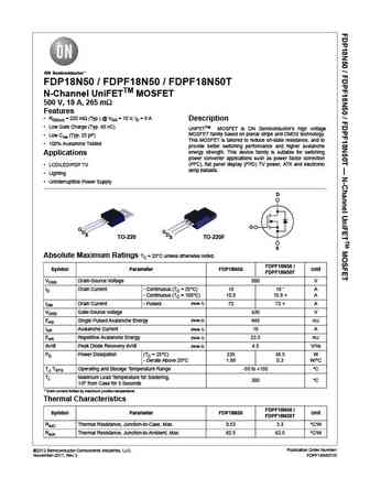
FDP18N50 / FDPF18N50 / FDPF18N50T N-Channel UniFETTM MOSFET 500 V, 18 A, 265 m Features RDS(on) = 220 m (Typ.) @ VGS = 10 V, ID = 9 A Description Low Gate Charge (Typ. 45 nC) UniFETTM MOSFET is ON Semiconductor s high voltage MOSFET family based on planar stripe and DMOS technology. Low Crss (Typ. 25 pF) This MOSFET is tailored to reduce on-state resistance, and to
0.9. Size:1033K onsemi
fdp18n50 fdpf18n50.pdf 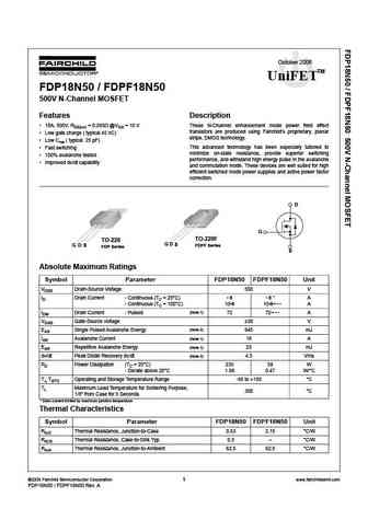
October 2006 TM UniFET FDP18N50 / FDPF18N50 500V N-Channel MOSFET Features Description 18A, 500V, RDS(on) = 0.265 @VGS = 10 V These N-Channel enhancement mode power field effect transistors are produced using Fairchild s proprietary, planar Low gate charge ( typical 45 nC) stripe, DMOS technology. Low Crss ( typical 25 pF) This advanced technology has been especially
0.10. Size:665K samhop
sdf18n50 sdp18n50.pdf 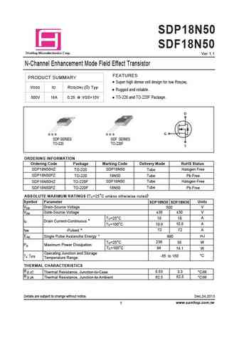
SDP18N50 SDF18N50 a S mHop Microelectronics C orp. Ver 1.1 N-Channel Enhancement Mode Field Effect Transistor FEATURES PRODUCT SUMMARY Super high dense cell design for low RDS(ON). VDSS ID RDS(ON) ( ) Typ Rugged and reliable. 500V 18A 0.25 @ VGS=10V TO-220 and TO-220F Package. D G G D S G D S SDP SERIES SDF SERIES TO-220 TO-220F S ORDERING INFORMATION Ordering Code Package M
0.11. Size:379K silikron
ssf18n50f.pdf 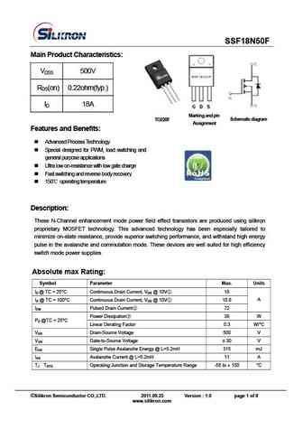
SSF18N50F Main Product Characteristics VDSS 500V RDS(on) 0.22ohm(typ.) ID 18A Marking and pin TO220F Schematic diagram Assignment Features and Benefits Advanced Process Technology Special designed for PWM, load switching and general purpose applications Ultra low on-resistance with low gate charge Fast switching and reverse body recovery 150 operating
0.14. Size:819K magnachip
mdf18n50.pdf 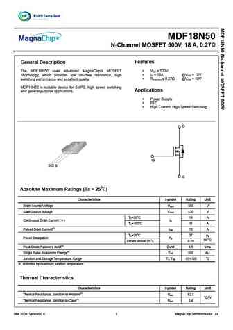
MDF18N50 N-Channel MOSFET 500V, 18 A, 0.27 General Description Features The MDF18N50 uses advanced MagnaChip s MOSFET V = 500V DS Technology, which provides low on-state resistance, high I = 18A @V = 10V D GS R 0.27 @V = 10V switching performance and excellent quality. DS(ON) GS MDF18N50 is suitable device for SMPS, high speed switching Applications and general
0.15. Size:1244K magnachip
mdf18n50bth mdp18n50bth.pdf 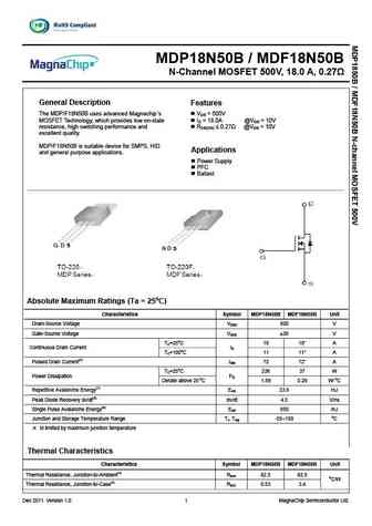
MDP18N50B / MDF18N50B N-Channel MOSFET 500V, 18.0 A, 0.27 General Description Features The MDP/F18N50B uses advanced Magnachip s VDS = 500V MOSFET Technology, which provides low on-state ID = 18.0A @VGS = 10V resistance, high switching performance and RDS(ON) 0.27 @VGS = 10V excellent quality. MDP/F18N50B is suitable device for SMPS, HID Applications and general
0.16. Size:964K bruckewell
msf18n50.pdf 
MSF18N50 500V N-Channel MOSFET Description The MSF18N50 is a N-channel enhancement-mode MOSFET, providing the designer with the best combination of fast switching, ruggedized device design, low on-resistance and cost effectiveness. he TO-220F package is universally preferred for all commercial-industrial applications Features Originative New Design Very Low Intrins
0.17. Size:608K winsemi
wff18n50.pdf 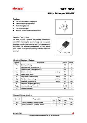
WFF18N50 WFF18N50 WFF18N50 WFF18N50 Silicon N-Channel MOSFET Silicon N-Channel MOSFET Silicon N-Channel MOSFET Silicon N-Channel MOSFET Features 18A,500V,R (Max0.27 )@V =10V DS(on) GS Ultra-low Gate charge(Typical 42nC) Fast Switching Capability 100%Avalanche Tested Maximum Junction Temperature Range(150 ) General Description This Power MOSFET is produced
0.18. Size:891K feihonltd
fhf18n50a.pdf 
N N-CHANNEL MOSFET FHF18N50A MAIN CHARACTERISTICS FEATURES ID 18A Low gate charge VDSS 500V Crss ( 23pF) Low Crss (typical 23pF ) Rdson-typ @Vgs=10V 0.31 Fast switching Qg-typ 58nC 100% 100% avalanche tested dv/dt Improved dv/d
0.19. Size:892K feihonltd
fhf18n50c.pdf 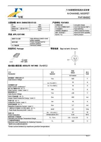
N N-CHANNEL MOSFET FHF18N50C MAIN CHARACTERISTICS FEATURES ID 18A Low gate charge VDSS 500V Crss ( 23pF) Low Crss (typical 23pF ) Rdson-typ @Vgs=10V 0.31 Fast switching Qg-typ 58nC 100% 100% avalanche tested dv/dt Improved dv/d
0.20. Size:1346K maple semi
slp18n50c slf18n50c.pdf 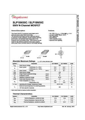
SLP18N50C / SLF18N50C 500V N-Channel MOSFET General Description Features This Power MOSFET is produced using Maple semi s - 18A, 500V, RDS(on)typ. = 236m @VGS = 10 V advanced planar stripe DMOS technology. - Low gate charge ( typical 69nC) This advanced technology has been especially tailored - High ruggedness to minimize on-state resistance, provide superior switching - Fast switching
0.21. Size:911K samwin
swf18n50d swt18n50d.pdf 
SW18N50D N-channel Enhanced mode TO-220F /TO-247 MOSFET TO-220F TO-247 BVDSS 500V Features ID 18A High ruggedness RDS(ON) 0.24 Low RDS(ON) (Typ 0.24 )@VGS=10V Low Gate Charge (Typ 88nC) 2 Improved dv/dt Capability 1 1 100% Avalanche Tested 2 2 1 3 3 Application LED , Charger, PC Power 1. Gate 2. Drain 3. Source 3 General
0.22. Size:652K samwin
sw18n50d swf18n50d swt18n50d.pdf 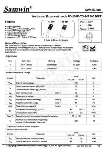
SW18N50D N-channel Enhanced mode TO-220F /TO-247 MOSFET TO-220F TO-247 BVDSS 500V Features ID 18A High ruggedness RDS(ON) 0.24 Low RDS(ON) (Typ 0.24 )@VGS=10V Low Gate Charge (Typ 88nC) 2 Improved dv/dt Capability 1 1 100% Avalanche Tested 2 2 1 3 3 Application LED , Charge, PC Power 1. Gate 2. Drain 3. Source 3 General D
0.23. Size:970K truesemi
tsf18n50mr.pdf 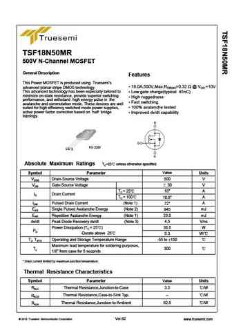
TSF18N50MR 500V N-Channel MOSFET General Description Features This Power MOSFET is produced using Truesemi s 18.0A,500V,Max.RDS(on)=0.32 @ VGS =10V advanced planar stripe DMOS technology. This advanced technology has been especially tailored to Low gate charge(typical 45nC) minimize on-state resistance, provide superior switching High ruggedness performance, and with
0.24. Size:1002K jiejie micro
jmpf18n50bj.pdf 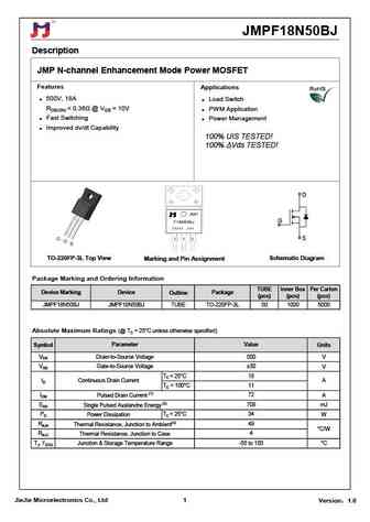
JMPF18N50BJ Description JMP N-channel Enhancement Mode Power MOSFET Features Applications 500V, 18A Load Switch RDS(ON)
0.25. Size:1558K cn sps
smirf18n50.pdf 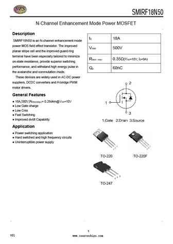
SMIRF18N50 30V /36A Single N Power MOSFET N-Channel Enhancement Mode Power MOSFET Description ID 18A SMIRF18N50 is an N-channel enhancement mode power MOS field effect transistor. The improved VDSS 500V planar stripe cell and the improved guard ring terminal have been especially tailored to minimize Rdson max 0.35 (VGS=10V, ID=9A) on-state resistance, provide superior
0.26. Size:245K inchange semiconductor
mdf18n50th.pdf 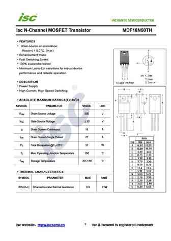
isc N-Channel MOSFET Transistor MDF18N50TH FEATURES Drain-source on-resistance RDS(on) 0.27 (max) Enhancement mode Fast Switching Speed 100% avalanche tested Minimum Lot-to-Lot variations for robust device performance and reliable operation DESCRITION Power Supply High Current, High Speed Switching ABSOLUTE MAXIMUM RATINGS(T =25 ) a SYMBOL PARAMETER
0.27. Size:245K inchange semiconductor
mdf18n50bth.pdf 
isc N-Channel MOSFET Transistor MDF18N50BTH FEATURES Drain-source on-resistance RDS(on) 0.27 (max) Enhancement mode Fast Switching Speed 100% avalanche tested Minimum Lot-to-Lot variations for robust device performance and reliable operation DESCRITION Power Supply High Current, High Speed Switching ABSOLUTE MAXIMUM RATINGS(T =25 ) a SYMBOL PARAMETER
Другие IGBT... DTG025N04NA, DTG045N04NA, DTG050P06LA, DTJ018N04N, F12N60, F13N50, F14N65, F16N65, IRLB3034, F18N65, F20N50, F20N60, F25N10, DHS042N15, DHS042N15E, DHS042N85P, DHS043N07P