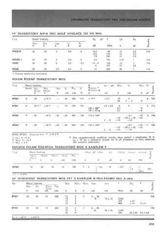
F630 datasheet, аналоги, основные параметры
Наименование производителя: F630 📄📄
Тип транзистора: MOSFET
Полярность: N
Предельные значения
Pd ⓘ - Максимальная рассеиваемая мощность: 38 W
|Vds|ⓘ - Максимально допустимое напряжение сток-исток: 200 V
|Vgs|ⓘ - Максимально допустимое напряжение затвор-исток: 30 V
|Id| ⓘ - Максимально допустимый постоянный ток стока: 9 A
Tj ⓘ - Максимальная температура канала: 150 °C
Электрические характеристики
tr ⓘ - Время нарастания: 3.5 ns
Cossⓘ - Выходная емкость: 94 pf
RDSonⓘ - Сопротивление сток-исток открытого транзистора: 0.28 Ohm
Тип корпуса: TO220F
📄📄 Копировать
Аналог (замена) для F630
- подборⓘ MOSFET транзистора по параметрам
F630 даташит
630 f630 i630 e630 b630 d630.pdf
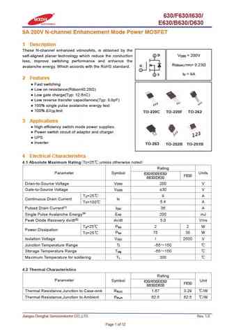
630/F630/I630/ E630/B630/D630 9A 200V N-channel Enhancement Mode Power MOSFET 1 Description These N-channel enhanced vdmosfets, is obtained by the 2 D V = 200V self-aligned planar technology which reduce the conduction DSS loss, improve switching performance and enhance the R = 0.23 DS(on) (TYP) G avalanche energy. Which accords with the RoHS standard. 1 I = 9A 3 S D 2 Feature

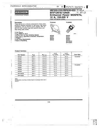
irf630b irfs630b.pdf

IRF630B/IRFS630B 200V N-Channel MOSFET General Description Features These N-Channel enhancement mode power field effect 9.0A, 200V, RDS(on) = 0.4 @VGS = 10 V transistors are produced using Fairchild s proprietary, Low gate charge ( typical 22 nC) planar, DMOS technology. Low Crss ( typical 22 pF) This advanced technology has been especially tailored to Fast switchin
irf630npbf irf630nspbf irf630nlpbf.pdf

PD - 95047A IRF630NPbF IRF630NSPbF l Advanced Process Technology IRF630NLPbF l Dynamic dv/dt Rating HEXFET Power MOSFET l 175 C Operating Temperature l Fast Switching D VDSS = 200V l Fully Avalanche Rated l Ease of Paralleling l Simple Drive Requirements RDS(on) = 0.30 G l Lead-Free Description ID = 9.3A Fifth Generation HEXFET Power MOSFETs from S International Rec
irf630nlpbf irf630npbf irf630nspbf irf630nstrrpbf.pdf
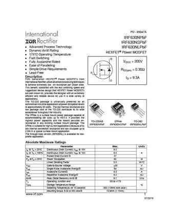
PD - 95047A IRF630NPbF IRF630NSPbF l Advanced Process Technology IRF630NLPbF l Dynamic dv/dt Rating HEXFET Power MOSFET l 175 C Operating Temperature l Fast Switching D VDSS = 200V l Fully Avalanche Rated l Ease of Paralleling l Simple Drive Requirements RDS(on) = 0.30 G l Lead-Free Description ID = 9.3A Fifth Generation HEXFET Power MOSFETs from S International Rec
irf630spbf.pdf
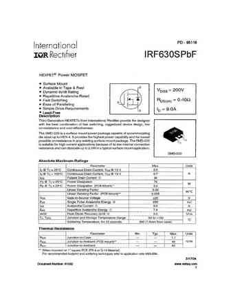
PD - 95118 IRF630SPbF Lead-Free 3/17/04 Document Number 91032 www.vishay.com 1 IRF630SPbF Document Number 91032 www.vishay.com 2 IRF630SPbF Document Number 91032 www.vishay.com 3 IRF630SPbF Document Number 91032 www.vishay.com 4 IRF630SPbF Document Number 91032 www.vishay.com 5 IRF630SPbF Document Number 91032 www.vishay.com 6 IRF630SPbF D2Pak Package Outli
irf630n.pdf
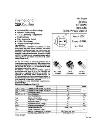
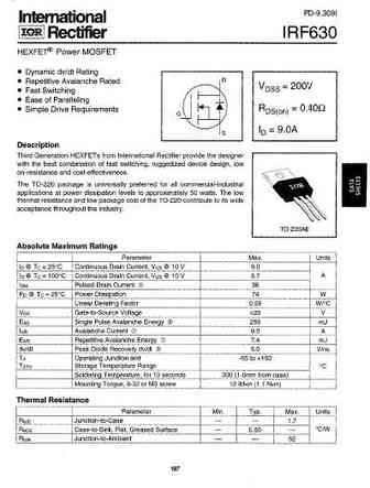
PD - 94005A IRF630N IRF630NS IRF630NL Advanced Process Technology HEXFET Power MOSFET Dynamic dv/dt Rating 175 C Operating Temperature D VDSS = 200V Fast Switching Fully Avalanche Rated RDS(on) = 0.30 Ease of Paralleling G Simple Drive Requirements Description ID = 9.3A Fifth Generation HEXFET Power MOSFETs from S International Rectifier utilize advanced proces
irf630pbf.pdf
PD- 95916 IRF630PbF Lead-Free 9/27/04 Document Number 91031 www.vishay.com 1 IRF630PbF Document Number 91031 www.vishay.com 2 IRF630PbF Document Number 91031 www.vishay.com 3 IRF630PbF Document Number 91031 www.vishay.com 4 IRF630PbF Document Number 91031 www.vishay.com 5 IRF630PbF Document Number 91031 www.vishay.com 6 IRF630PbF Peak Diode Recovery dv/dt T
irf630 s 1.pdf
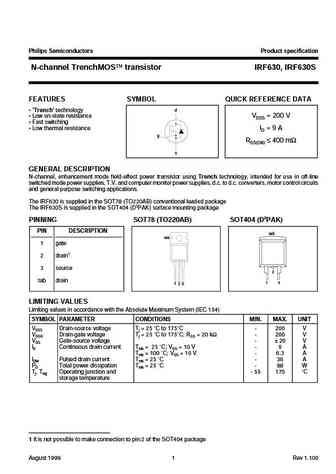
Philips Semiconductors Product specification N-channel TrenchMOS transistor IRF630, IRF630S FEATURES SYMBOL QUICK REFERENCE DATA Trench technology d Low on-state resistance VDSS = 200 V Fast switching Low thermal resistance ID = 9 A g RDS(ON) 400 m s GENERAL DESCRIPTION N-channel, enhancement mode field-effect power transistor using Trench technology
irf630.pdf
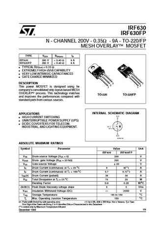
IRF630 IRF630FP N - CHANNEL 200V - 0.35 - 9A - TO-220/FP MESH OVERLAY MOSFET TYPE VDSS RDS(on) ID IRF630 200 V
irf630mfp.pdf
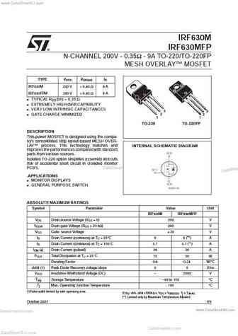
www.DataSheet4U.com IRF630M IRF630MFP N-CHANNEL 200V - 0.35 - 9A TO-220/TO-220FP MESH OVERLAY MOSFET TYPE VDSS RDS(on) ID IRF630M 200 V
irf630m.pdf
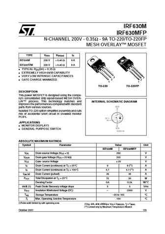
IRF630M IRF630MFP N-CHANNEL 200V - 0.35 - 9A TO-220/TO-220FP MESH OVERLAY MOSFET TYPE VDSS RDS(on) ID IRF630M 200 V
irf630s.pdf
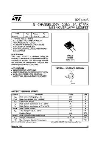
IRF630S N - CHANNEL 200V - 0.35 - 9A- D2PAK MESH OVERLAY MOSFET TYPE VDSS RDS(on) ID IRF630S 200 V
irf630 irf630fp.pdf
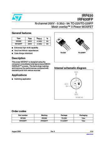
IRF630 IRF630FP N-channel 200V - 0.35 - 9A TO-220/TO-220FP Mesh overlay II Power MOSFET General features Type VDSS RDS(on) ID IRF630 200V
fqpf630.pdf
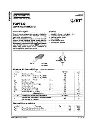
April 2000 TM QFET QFET QFET QFET 200V N-ChanneI MOSFET GeneraI Description Features These N-Channel enhancement mode power field effect 6.3A, 200V, RDS(on) = 0.4 @VGS = 10 V transistors are produced using Fairchild s proprietary, Low gate charge ( typical 19 nC) planar stripe, DMOS technology. Low Crss ( typical 35 pF) This advanced technology has been es

irf630 rf1s630sm.pdf
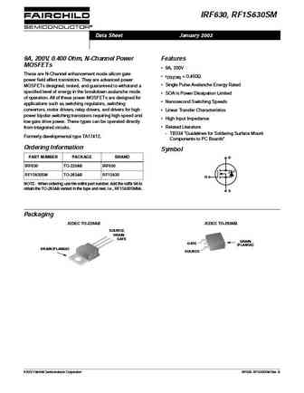
IRF630, RF1S630SM Data Sheet January 2002 9A, 200V, 0.400 Ohm, N-Channel Power Features MOSFETs 9A, 200V These are N-Channel enhancement mode silicon gate rDS(ON) = 0.400 power field effect transistors. They are advanced power Single Pulse Avalanche Energy Rated MOSFETs designed, tested, and guaranteed to withstand a specified level of energy in the breakdown avalanc
irf630b.pdf
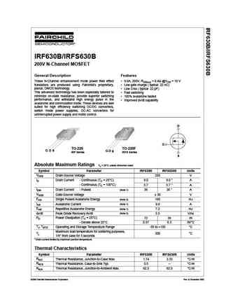
IRF630B/IRFS630B 200V N-Channel MOSFET General Description Features These N-Channel enhancement mode power field effect 9.0A, 200V, RDS(on) = 0.4 @VGS = 10 V transistors are produced using Fairchild s proprietary, Low gate charge ( typical 22 nC) planar, DMOS technology. Low Crss ( typical 22 pF) This advanced technology has been especially tailored to Fast switchin
irf630a.pdf
Advanced Power MOSFET FEATURES BVDSS = 200 V Avalanche Rugged Technology RDS(on) = 0.4 Rugged Gate Oxide Technology Lower Input Capacitance ID = 9 A Improved Gate Charge Extended Safe Operating Area Lower Leakage Current 10 A (Max.) @ VDS = 200V Low RDS(ON) 0.333 (Typ.) 1 2 3 1.Gate 2. Drain 3. Source Absolute Maximum Ratings Symbol Characteristic Value
irf630spbf sihf630s.pdf
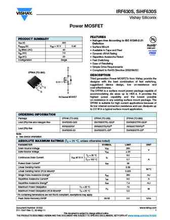
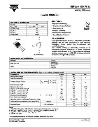
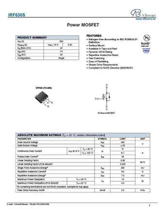
IRF630S, SiHF630S Vishay Siliconix Power MOSFET FEATURES PRODUCT SUMMARY Halogen-free According to IEC 61249-2-21 VDS (V) 200 Definition RDS(on) ( )VGS = 10 V 0.40 Surface Mount Qg (Max.) (nC) 43 Available in Tape and Reel Qgs (nC) 7.0 Dynamic dV/dt Rating Qgd (nC) 23 Repetitive Avalanche Rated Configuration Single Fast Switching Ease of Paralleli
irf630pbf sihf630.pdf
IRF630, SiHF630 Vishay Siliconix Power MOSFET FEATURES PRODUCT SUMMARY Dynamic dV/dt Rating VDS (V) 200 Available Repetitive Avalanche Rated RDS(on) ( )VGS = 10 V 0.40 RoHS* Fast Switching Qg (Max.) (nC) 43 COMPLIANT Ease of Paralleling Qgs (nC) 7.0 Qgd (nC) 23 Simple Drive Requirements Configuration Single Compliant to RoHS Directive 2002/95/EC D D
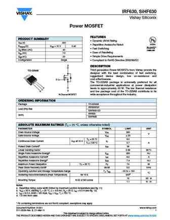
irf630 sihf630.pdf
IRF630, SiHF630 Vishay Siliconix Power MOSFET FEATURES PRODUCT SUMMARY Dynamic dV/dt Rating VDS (V) 200 Repetitive Avalanche Rated Available RDS(on) ( )VGS = 10 V 0.40 Fast Switching RoHS* Qg (Max.) (nC) 43 COMPLIANT Ease of Paralleling Qgs (nC) 7.0 Qgd (nC) 23 Simple Drive Requirements Configuration Single Lead (Pb)-free Available D DESCRIPTION TO-
irf630s sihf630s.pdf

IRF630S, SiHF630S Vishay Siliconix Power MOSFET FEATURES PRODUCT SUMMARY Halogen-free According to IEC 61249-2-21 VDS (V) 200 Definition RDS(on) ( )VGS = 10 V 0.40 Surface Mount Qg (Max.) (nC) 43 Available in Tape and Reel Qgs (nC) 7.0 Dynamic dV/dt Rating Qgd (nC) 23 Repetitive Avalanche Rated Configuration Single Fast Switching Ease of Paralleli
uf630l-tm3-t uf630g-tm3-t uf630l-tn3-r uf630g-tn3-r uf630l-t2q-t uf630g-t2q-t uf630g-s08-r.pdf

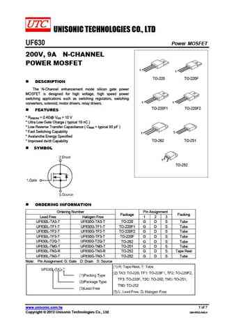
UNISONIC TECHNOLOGIES CO., LTD UF630 Power MOSFET 200V, 9A N-CHANNEL POWER MOSFET 1 1 TO-220 TO-220F DESCRIPTION The N-Channel enhancement mode silicon gate power MOSFET is designed for high voltage, high speed power 1 1 switching applications such as switching regulators, switching converters, solenoid, motor drivers, relay drivers. TO-220F1 TO-220F2 FEATURES
uf630.pdf
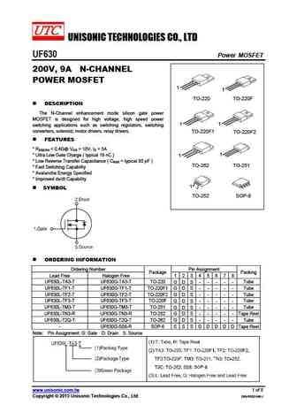
UNISONIC TECHNOLOGIES CO., LTD UF630 Power MOSFET 200V, 9A N-CHANNEL POWER MOSFET 1 1 TO-220 TO-220F DESCRIPTION The N-Channel enhancement mode silicon gate power MOSFET is designed for high voltage, high speed power switching applications such as switching regulators, switching 1 1 converters, solenoid, motor drivers, relay drivers. TO-220F1 TO-220F2 FEATURES
uf630l-ta3-t uf630g-ta3-t uf630l-tf1-t uf630g-tf1-t uf630l-tf2-t uf630g-tf2-t uf630l-tf3-t uf630g-tf3-t.pdf
UNISONIC TECHNOLOGIES CO., LTD UF630 Power MOSFET 200V, 9A N-CHANNEL POWER MOSFET 1 1 TO-220 TO-220F DESCRIPTION The N-Channel enhancement mode silicon gate power MOSFET is designed for high voltage, high speed power 1 1 switching applications such as switching regulators, switching converters, solenoid, motor drivers, relay drivers. TO-220F1 TO-220F2 FEATURES
mrf630.pdf
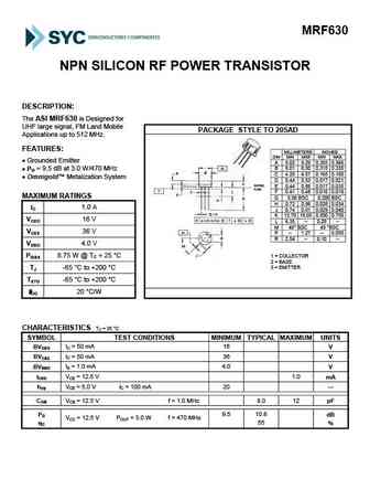
MRF630 NPN SILICON RF POWER TRANSISTOR DESCRIPTION The ASI MRF630 is Designed for UHF large signal, FM Land Mobile PACKAGE STYLE TO 205AD Applications up to 512 MHz. FEATURES MILLIMETERS INCHES DIM MIN MAX MIN MAX Grounded Emitter A 9.02 9.29 0.355 0.366 B 8.01 8.50 0.315 0.335 PG = 9.5 dB at 3.0 W/470 MHz C 4.20 4.57 0.165 0.180 Omnigold Metalization Sys
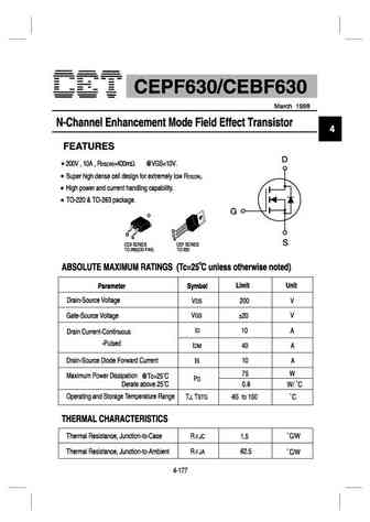
cep630n ceb630n cef630n.pdf
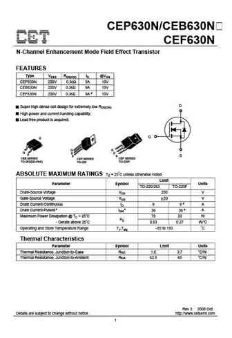
CEP630N/CEB630N CEF630N N-Channel Enhancement Mode Field Effect Transistor FEATURES Type VDSS RDS(ON) ID @VGS CEP630N 200V 0.36 9A 10V CEB630N 200V 0.36 9A 10V CEF630N 200V 0.36 9A d 10V D Super high dense cell design for extremely low RDS(ON). High power and current handing capability. Lead free product is acquired. G S CEB SERIES CEP SERIES CEF SERIES TO-263(DD-PAK)
hirf630.pdf
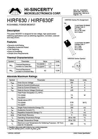
Spec. No. MOS200401 HI-SINCERITY Issued Date 2004.04.01 Revised Date 2005.04.22 MICROELECTRONICS CORP. Page No. 1/6 HIRF630 Series Pin Assignment HIRF630 / HIRF630F Tab N-CHANNEL POWER MOSFET 3-Lead Plastic TO-220AB Package Code E Pin 1 Gate Pin 2 & Tab Drain Description Pin 3 Source This power MOSFET is designed for low voltage, high speed power switching applicati
irf630.pdf
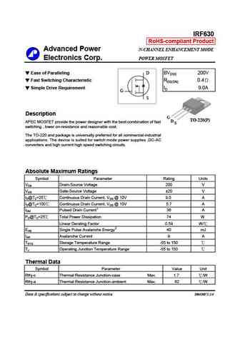
IRF630 RoHS-compliant Product Advanced Power N-CHANNEL ENHANCEMENT MODE Electronics Corp. POWER MOSFET Ease of Paralleling D BVDSS 200V Fast Switching Characteristic RDS(ON) 0.4 Simple Drive Requirement ID 9.0A G S Description G TO-220(P) D APEC MOSFET provide the power designer with the best combination of fast S switching , lower on-resistance and reasonable cost.
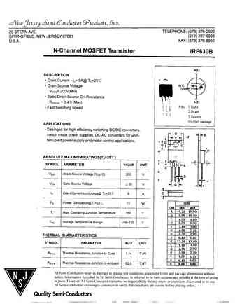
irf630h.pdf
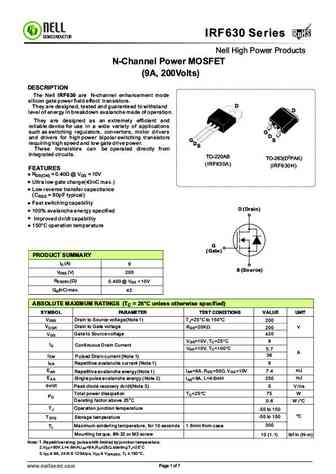
RoHS IRF630 Series RoHS SEMICONDUCTOR Nell High Power Products N-Channel Power MOSFET (9A, 200Volts) DESCRIPTION The Nell IRF630 are N-channel enhancement mode silicon gate power field effect transistors. D They are designed, tested and guaranteed to withstand D level of energy in breakdown avalanche made of operation. They are designed as an extremely efficient and reliab
hff630.pdf
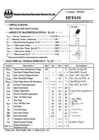
N-Channel MOSFET Shantou Huashan Electronic Devices Co.,Ltd. HFF630 APPLICATIONSL TO-220F High Voltage High-Speed Switching. ABSOLUTE MAXIMUM RATINGS Ta=25 1 Tstg Storage Temperature -55 150 1 G Tj Operating Junction Temperature 150 2 D PD Allowable Power Dissipatio
irf630s.pdf
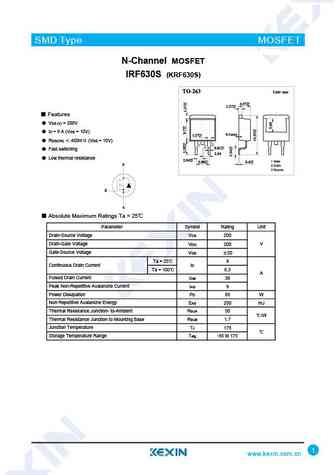
SMD Type MOSFET N-Channel MOSFET IRF630S (KRF630S) Features VDS (V) = 200V ID = 9 A (VGS = 10V) RDS(ON) 400m (VGS = 10V) Fast switching Low thermal resistance d g s Absolute Maximum Ratings Ta = 25 Parameter Symbol Rating Unit Drain-Source Voltage VDS 200 V Drain-Gate Voltage VDG 200 Gate-Source Voltage VGS 20 Ta = 25 9 Cont
wff630.pdf
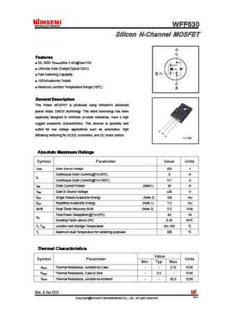
WFF630 WFF630 WFF630 WFF630 Silicon N-Channel MOSFET Silicon N-Channel MOSFET Silicon N-Channel MOSFET Silicon N-Channel MOSFET Features Features Features Features 9A, 200V, R (Max 0.4 )@V =10V DS(on) GS Ultra-low Gate Charge(Typical 22nC) Fast Switching Capability 100%Avalanche Tested Maximum Junction Temperature Range(150 ) General Description General
fhu630a fhd630a fhp630a fhf630a.pdf
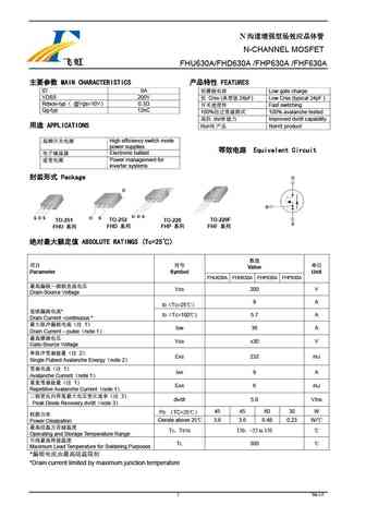
N N-CHANNEL MOSFET FHU630A/FHD630A /FHP630A /FHF630A MAIN CHARACTERISTICS FEATURES ID 9A Low gate charge VDSS 200V Crss ( 24pF) Low Crss (typical 24pF ) Rdson-typ @Vgs=10V 0.3 Fast switching Qg-typ 12nC 100% 100% avalanche tested dv/d
sw630 swp630 swf630 swd630.pdf
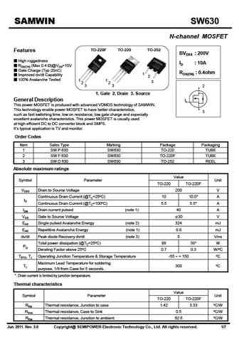
SAMWIN SW630 N-channel MOSFET TO-220F TO-220 TO-252 Features BVDSS 200V High ruggedness ID 10A RDS(ON) (Max 0.4 )@VGS=10V Gate Charge (Typ 20nC) RDS(ON) 0.4ohm 1 Improved dv/dt Capability 2 100% Avalanche Tested 1 1 3 2 2 3 3 2 1. Gate 2. Drain 3. Source General Description 1 This power MOSFET is produced with advanced VDMOS technology of SAMW
tmp630z tmpf630z.pdf
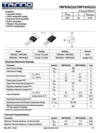
TMP630Z(G)/TMPF630Z(G) N-channel MOSFET Features Low gate charge BVDSS ID RDS(on)MAX 100% avalanche tested 200V 9A
jmpf630bj.pdf
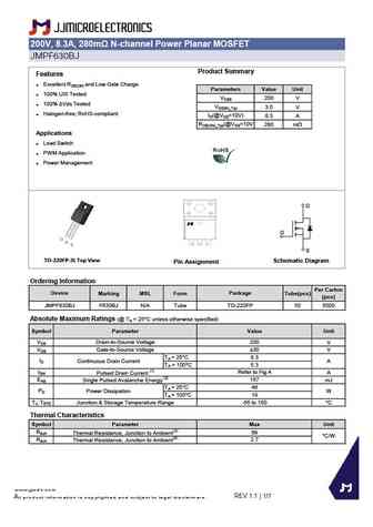
200V, 8.3A, 280m N-channel Power Planar MOSFET JMPF630BJ Product Summary Features Excellent RDS(ON) and Low Gate Charge Parameters Value Unit 100% UIS Tested VDSS 200 V 100% Vds Tested VGS(th)_Typ 3.0 V Halogen-free; RoHS-compliant ID(@VGS=10V) 8.3 A RDS(ON)_Typ(@VGS=10V 280 mW Applications Load Switch PWM Application Power Management D G S
irf630mfp.pdf
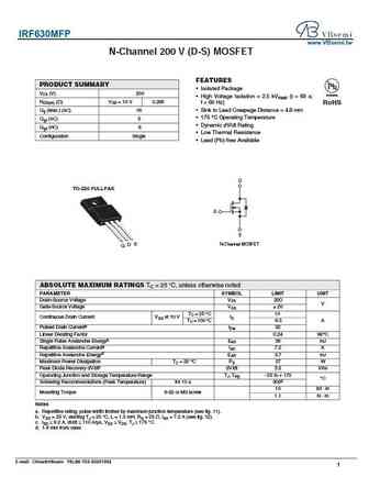
IRF630MFP www.VBsemi.tw N-Channel 200 V (D-S) MOSFET FEATURES PRODUCT SUMMARY Isolated Package VDS (V) 200 Available High Voltage Isolation = 2.5 kVRMS (t = 60 s; RDS(on) ( )VGS = 10 V 0.265 f = 60 Hz) RoHS Qg (Max.) (nC) 16 Sink to Lead Creepage Distance = 4.8 mm 175 C Operating Temperature Qgs (nC) 5 Dynamic dV/dt Rating Qgd (nC) 8 Low Thermal Resist
irf630p.pdf
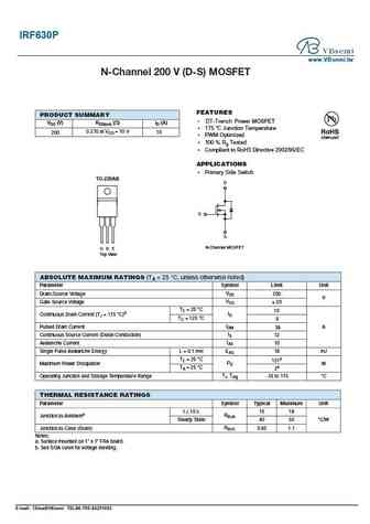
IRF630P www.VBsemi.tw N-Channel 200 V (D-S) MOSFET FEATURES PRODUCT SUMMARY DT-Trench Power MOSFET VDS (V) RDS(on) ( )ID (A) 175 C Junction Temperature 0.270 at VGS =10V 10 200 PWM Optimized 100 % Rg Tested Compliant to RoHS Directive 2002/95/EC APPLICATIONS Primary Side Switch TO-220AB D G S N-Channel MOSFET G D S Top View ABSOLUTE MAXIMUM RATI
irf630s.pdf
IRF630S www.VBsemi.tw Power MOSFET FEATURES PRODUCT SUMMARY Halogen-free According to IEC 61249-2-21 VDS (V) 200 Definition RDS(on) ( )VGS = 10 V 0.30 Surface Mount Qg (Max.) (nC) 43 Available in Tape and Reel Qgs (nC) 7.0 Dynamic dV/dt Rating Qgd (nC) 23 Repetitive Avalanche Rated Configuration Single Fast Switching Ease of Paralleling Simpl
ytf630.pdf
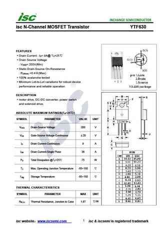
isc N-Channel MOSFET Transistor YTF630 FEATURES Drain Current I = 9A@ T =25 D C Drain Source Voltage V = 200V(Min) DSS Static Drain-Source On-Resistance R =0.4 (Max) DS(on) 100% avalanche tested Minimum Lot-to-Lot variations for robust device performance and reliable operation DESCRIPTION motor drive, DC-DC converter, power switch and solenoid drive. ABSOLU
irf630.pdf
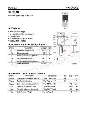
MOSFET INCHANGE IRF630 N-channel mosfet transistor Features 1 2 3 With TO-220 package Low on-state and thermal resistance Fast switching VDSS=200V; RDS(ON) 0.4 ;ID=9A 1.gate 2.drain 3.source Absolute Maximum Ratings Tc=25 SYMBOL PARAMETER RATING UNIT VDSS Drain-source voltage (VGS=0) 200 V VGS Gate-source voltage 20 V ID Drain Current-continuous@ TC
irf630b.pdf
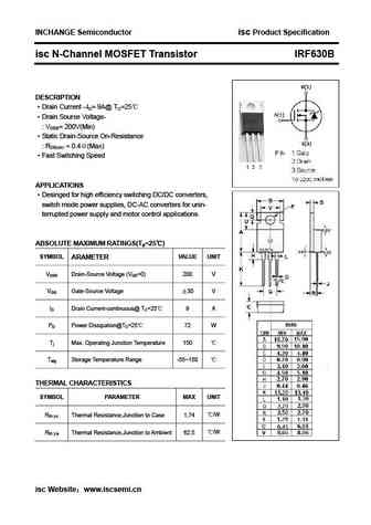
INCHANGE Semiconductor isc Product Specification isc N-Channel MOSFET Transistor IRF630B DESCRIPTION Drain Current ID= 9A@ TC=25 Drain Source Voltage- VDSS= 200V(Min) Static Drain-Source On-Resistance RDS(on) = 0.4 (Max) Fast Switching Speed APPLICATIONS Desinged for high efficiency switching DC/DC converters, switch mode power supplies, DC-AC conve
irf630a.pdf
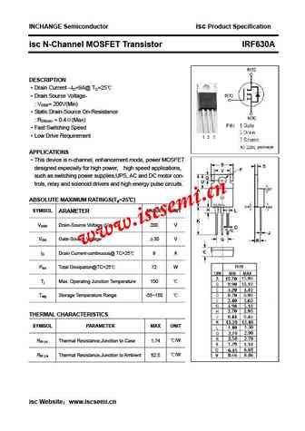
INCHANGE Semiconductor isc Product Specification isc N-Channel MOSFET Transistor IRF630A DESCRIPTION Drain Current ID=9A@ TC=25 Drain Source Voltage- VDSS= 200V(Min) Static Drain-Source On-Resistance RDS(on) = 0.4 (Max) Fast Switching Speed Low Drive Requirement APPLICATIONS This device is n-channel, enhancement mode, power MOSFET designed espec
irf630nl.pdf
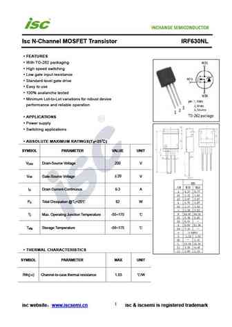
Isc N-Channel MOSFET Transistor IRF630NL FEATURES With TO-262 packaging High speed switching Low gate input resistance Standard level gate drive Easy to use 100% avalanche tested Minimum Lot-to-Lot variations for robust device performance and reliable operation APPLICATIONS Power supply Switching applications ABSOLUTE MAXIMUM RATINGS(T =25 ) a SYMBOL PAR
irf630nstrrpbf.pdf
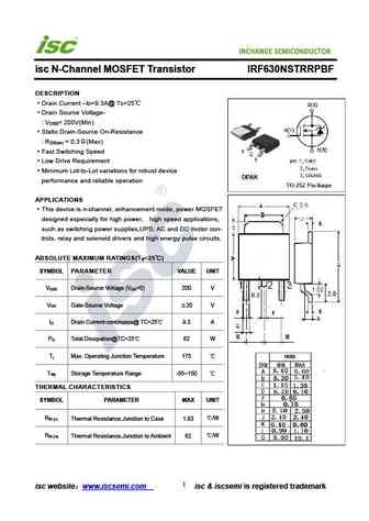
INCHANGE Semiconductor isc N-Channel MOSFET Transistor IRF630NSTRRPBF DESCRIPTION Drain Current I =9.3A@ T =25 D C Drain Source Voltage- V = 200V(Min) DSS Static Drain-Source On-Resistance R = 0.3 (Max) DS(on) Fast Switching Speed Low Drive Requirement Minimum Lot-to-Lot variations for robust device performance and reliable operation APPLICATIONS This de
irf630ns.pdf
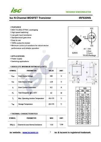
Isc N-Channel MOSFET Transistor IRF630NS FEATURES With TO-263( D PAK ) packaging High speed switching Low gate input resistance Standard level gate drive Easy to use 100% avalanche tested Minimum Lot-to-Lot variations for robust device performance and reliable operation APPLICATIONS Power supply Switching applications ABSOLUTE MAXIMUM RATINGS(T =25 ) a
irf630n.pdf
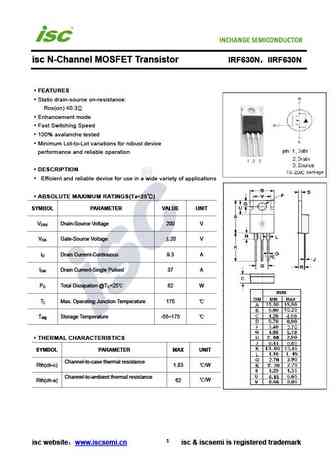
isc N-Channel MOSFET Transistor IRF630N IIRF630N FEATURES Static drain-source on-resistance RDS(on) 0.3 Enhancement mode Fast Switching Speed 100% avalanche tested Minimum Lot-to-Lot variations for robust device performance and reliable operation DESCRIPTION Efficient and reliable device for use in a wide variety of applications ABSOLUTE MAXIMUM RATINGS(T
irf630f.pdf
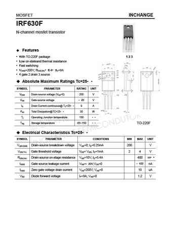
MOSFET INCHANGE IRF630F N-channel mosfet transistor Features With TO-220F package 1 2 3 Low on-stateand thermal resistance Fast switching VDSS=200V; RDS(ON) 0.4 ;ID=9A 1.gate 2.drain 3.source Absolute Maximum Ratings Tc=25 SYMBOL PARAMETER RATING UNIT VDSS Drain-source voltage (VGS=0) 200 V VGS Gate-source voltage 20 V ID Drain Current-continuous@ TC
Другие IGBT... DSE022N10N3, F4N60, F4N65, F4N70, F50N06, F50N20, F5N65C, F5N80, 8205A, F640, F6N90, F740, F7N60, F7N70, F7N80, F80N06, F8N50
Параметры MOSFET. Взаимосвязь и компромиссы
History: SUN05A50ZF | CEB3205
🌐 : EN ES РУ

Список транзисторов
Обновления
MOSFET: MSH100N045SA | MSD60P16 | MSD40P45 | MSB100N023 | MS60P03 | MS40P05AU | MS40P05 | MS40N05 | MS34P07 | MS34P01 | MS23P03 | MS23N06A | BPMS04N003M | BPM0405CG | BPM0306CG | BP0405SCG
Popular searches
a1023 | d313 transistor | 2sa1302 | 2sd315 | a1013 | 2sb554 | 2sd2560 | 2sc2078 transistor