AGM314MD. Аналоги и основные параметры
Наименование производителя: AGM314MD
Тип транзистора: MOSFET
Полярность: NP
Предельные значения
Pd ⓘ
- Максимальная рассеиваемая мощность: 29.7 W
|Vds|ⓘ - Максимально допустимое напряжение сток-исток: 30 V
|Vgs|ⓘ - Максимально допустимое напряжение затвор-исток: 20 V
|Id| ⓘ - Максимально допустимый постоянный ток стока: 30(20) A
Tj ⓘ - Максимальная температура канала: 150 °C
Электрические характеристики
tr ⓘ -
Время нарастания: 25(5) ns
Cossⓘ - Выходная емкость: 99(101) pf
RDSonⓘ - Сопротивление сток-исток открытого транзистора: 0.015(0.026) Ohm
Тип корпуса: TO252-4L
Аналог (замена) для AGM314MD
- подборⓘ MOSFET транзистора по параметрам
AGM314MD даташит
..1. Size:1636K cn agmsemi
agm314md.pdf 
AGM314MD Table 3. P-Channel Electrical Characteristics (TJ=25 unless otherwisenoted) Symbol Parameter Conditions Min Typ Max Unit On/Off States BVDSS Drain-Source Breakdown Voltage VGS=0V ID=-250 A -30 -- -- V Zero Gate Voltage Drain Current V =-30V,V =0V -1 DS GS I -- -- A DSS Gate-Body Leakage Current V = 20V,V =0V 100 GS DS I -- -- nA GSS V Gate Threshold Voltage V =V
7.1. Size:1921K cn agmsemi
agm314ma.pdf 
AGM314MA Table 3. N- Channel Electrical Characteristics (TJ=25 unless otherwisenoted) Symbol Parameter Conditions Min Typ Max Unit On/Off States BV Drain-Source Breakdown Voltage V =0V I =250 A 30 -- -- V GS D DSS Zero Gate Voltage Drain Current V =30V,V =0V -- -- 1 A DS GS I DSS Gate-Body Leakage Current V = 20V,V =0V -- -- nA GS DS 100 I GSS VGS(th) Gate Threshold Vo
7.2. Size:1622K cn agmsemi
agm314map.pdf 
AGM314MAP Table 3. P-Channel Electrical Characteristics (TJ=25 unless otherwisenoted) Symbol Parameter Conditions Min Typ Max Unit On/Off States BVDSS Drain-Source Breakdown Voltage VGS=0V ID=-250 A -30 -- -- V Zero Gate Voltage Drain Current V =-30V,V =0V -1 DS GS I -- -- A DSS Gate-Body Leakage Current V = 20V,V =0V 100 GS DS I -- -- nA GSS V Gate Threshold Voltage V =
9.1. Size:865K cn agmsemi
agm310as.pdf 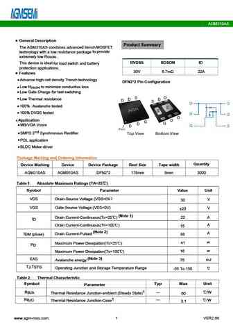
AGM310AS General Description Product Summary The AGM310AS combines advanced trench MOSFET to provide technology with a low resistance package extremely low R . DS(ON) BVDSS RDSON ID This device is ideal for load switch and battery protection applications. 30V 6.7m 22A Features Advance high cell density Trench technology DFN2*2 Pin Configuration Low R to minimi
9.2. Size:1137K cn agmsemi
agm318map.pdf 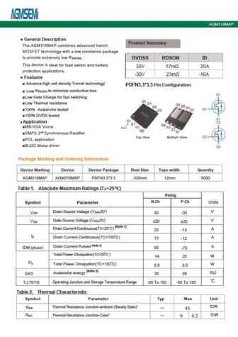
AGM318MAP Table 3. N- Channel Electrical Characteristics (TJ=25 unless otherwisenoted) Symbol Parameter Conditions Min Typ Max Unit On/Off States BV Drain-Source Breakdown Voltage V =0V I =250 A 30 -- -- V GS D DSS Zero Gate Voltage Drain Current V =30V,V =0V -- -- 1 A DS GS I DSS Gate-Body Leakage Current V = 20V,V =0V -- -- nA GS DS 100 I GSS VGS(th) Gate Threshold V
9.3. Size:1449K cn agmsemi
agm312map.pdf 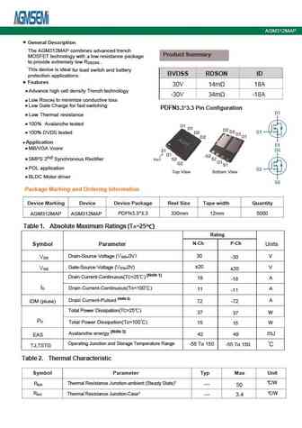
AGM312MAP Table 3. P-Channel Electrical Characteristics (TJ=25 unless otherwisenoted) Symbol Parameter Conditions Min Typ Max Unit On/Off States BVDSS Drain-Source Breakdown Voltage VGS=0V ID=-250 A -30 -- -- V Zero Gate Voltage Drain Current V =-24V,V =0V -1 DS GS I -- -- A DSS Gate-Body Leakage Current V = 20V,V =0V 100 GS DS I -- -- nA GSS V Gate Threshold Voltage V =
9.4. Size:1388K cn agmsemi
agm310map.pdf 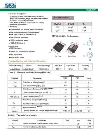
AGM310MAP Table 3. N- Channel Electrical Characteristics (TJ=25 unless otherwisenoted) Symbol Parameter Conditions Min Typ Max Unit On/Off States BV Drain-Source Breakdown Voltage V =0V I =250 A 30 -- -- V GS D DSS Zero Gate Voltage Drain Current V =30V,V =0V -- -- 1 A DS GS I DSS Gate-Body Leakage Current V = 20V,V =0V -- -- nA GS DS 100 I GSS VGS(th) Gate Threshold V
9.5. Size:1521K cn agmsemi
agm310ma.pdf 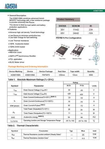
AGM310MA N Channel characteristics curve Fig.1 Power Dissipation Derating Curve Fig.2 Typical output Characteristics 1.2 50 1 V =10V GS 0.8 V =4.5V GS 25 0.6 0.4 0.2 0 0 0.5 1 1.5 2 0 Drain-Source voltage (V) 0 50 100 150 200 Temperature ( C) Fig.3 Threshold Voltage V.S Junction Temperature Fig.4 Resistance V.S Drain Current 2.5 20 2 1.5 10 1 0.5 0 0 -5
9.6. Size:615K cn agmsemi
agm310a.pdf 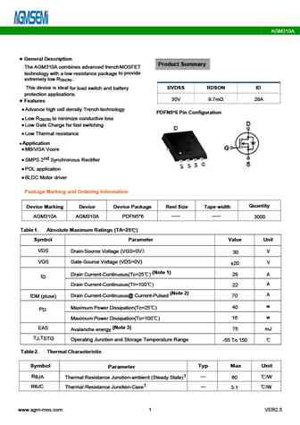
AGM310A General Description Product Summary The AGM310A combines advanced trenchMOSFET to provide technology with a low resistance package extremely low R . DS(ON) This device is ideal BVDSS RDSON ID for load switch and battery protection applications. 30V 9.7m 28A Features Advance high cell density Trench technology PDFN5*6 Pin Configuration Low R to minimize
9.7. Size:902K cn agmsemi
agm310d.pdf 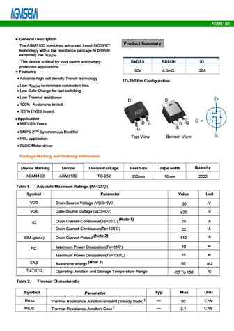
AGM310D Table 3. Electrical Characteristics (Tj=25 unless otherwise noted) Symbol Parameter Conditions Min Typ Max Unit On/Off States BV Drain-Source Breakdown Voltage V =0V I =250 A 30 -- -- V GS D DSS Zero Gate Voltage Drain Current V =30V,V =0V -- -- 1.0 A DS GS I DSS Gate-Body Leakage Current V = 20V,V =0V -- -- nA GS DS I GSS 100 V Gate Threshold Voltage V =V ,I
9.8. Size:807K cn agmsemi
agm315mbp.pdf 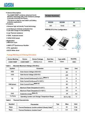
AGM315MBP Table 3. Electrical Characteristics (TJ=25 unless otherwise noted) Symbol Parameter Conditions Min Typ Max Unit On/Off States BVDSS Drain-Source Breakdown Voltage V =0V I =250 A 30 -- -- V GS D Zero Gate Voltage Drain Current V =30V,V =0V -- -- 1 A DS GS I DSS V = 20V,V =0V -- -- nA GS DS IGSS Gate-Body Leakage Current 100 VGS(th) Gate Threshold Voltage V =V
9.9. Size:1429K cn agmsemi
agm310m.pdf 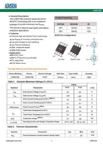
AGM310M General Description Product Summary The AGM310M combines advanced trench MOSFET technology with a low resistance to provide extremely low R . BVDSS RDSON ID package DS(ON) This device is ideal for load switch and battery 30V 12m 12A protection applications. -30V 16m -12A Features SOP8 Pin Configuration Advance high cell density Trench technology R to minimi
9.10. Size:1450K cn agmsemi
agm310mar.pdf 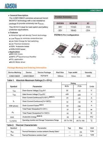
AGM310MAR Table 3. N- Channel Electrical Characteristics (TJ=25 unless otherwisenoted) Symbol Parameter Conditions Min Typ Max Unit On/Off States BV Drain-Source Breakdown Voltage V =0V I =250 A 30 -- -- V GS D DSS Zero Gate Voltage Drain Current V =30V,V =0V -- -- 1 A DS GS I DSS Gate-Body Leakage Current V = 20V,V =0V -- -- nA GS DS 100 I GSS VGS(th) Gate Threshold V
9.11. Size:802K cn agmsemi
agm318d.pdf 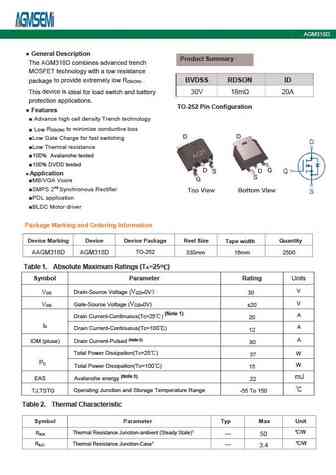
AGM318D 25 20 VGS= 5 10V 20 16 VGS 4V 15 12 10 8 5 4 VGS 3V 0 0 0 1 2 3 4 5 6 0 1 2 3 4 5 6 VDS , Drain-to-Source Voltage (V) VGS , Gate-to-Source Voltage (V) Figure 1. Output Characteristics Figure 2. Transfer Characteristics 1.1 2 VG = 10V ID= 250uA 1.075 1.75 ID= 6.9A 1.05 1.5 1.025 1.25 1 1 0.975 0.75 0.95 0.5 0.925 0.25 -50 -25 0 25 50 75 100 12
9.12. Size:1295K cn agmsemi
agm310md.pdf 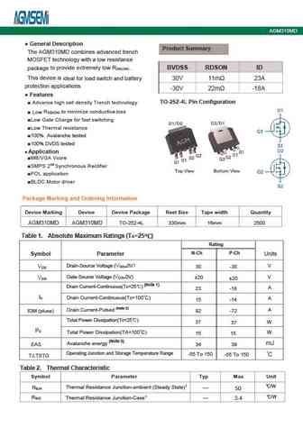
AGM310MD Table 3. N- Channel Electrical Characteristics (Tj=25 unless otherwisenoted) Symbol Parameter Conditions Min Typ Max Unit On/Off States BV Drain-Source Breakdown Voltage V =0V I =250 A 30 -- -- V GS D DSS Zero Gate Voltage Drain Current V =30V,V =0V -- -- 1 A DS GS I DSS Gate-Body Leakage Current V = 20V,V =0V -- -- nA GS DS 100 I GSS VGS(th) Gate Threshold Vo
9.13. Size:914K cn agmsemi
agm311map.pdf 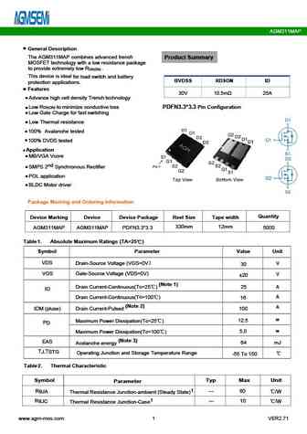
AGM311MAP General Description The AGM311MAP combines advanced trench Product Summary MOSFET technology with a low resistance package to provide extremely low R . DS(ON) This device is ideal for load switch and battery BVDSS RDSON ID protection applications. Features 30V 10.5m 25A Advance high cell density Trench technology Low R to minimize conductive loss PDFN3
9.14. Size:788K cn agmsemi
agm318mn.pdf 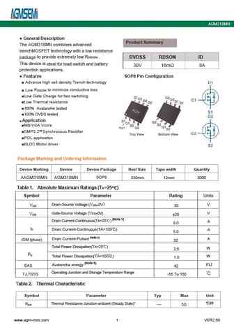
AGM318MN General Description Product Summary The AGM318MN combines advanced trenchMOSFET technology with a low resistance to provide extremely low R . package DS(ON) BVDSS RDSON ID This device is ideal for load switch and battery 30V 16m 8A protection applications. Features SOP8 Pin Configuration Advance high cell density Trench technology R to minimize conductive lo
9.15. Size:1126K cn agmsemi
agm312m2.pdf 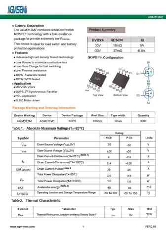
AGM312M2 General Description Product Summary The AGM312M2 combines advanced trench MOSFET technology with a low resistance to provide extremely low R . package DS(ON) BVDSS RDSON ID This device is ideal for load switch and battery 30V 18m 9A protection applications. -30V 37m -6.8A Features Advance high cell density Trench technology SOP8 Pin Configuration Low R t
9.16. Size:932K cn agmsemi
agm312d.pdf 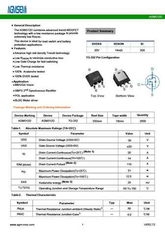
AGM312D General Description The AGM312D combines advanced trench MOSFET Product Summary to provide technology with a low resistance package extremely low R . DS(ON) This device is ideal for load switch and battery BVDSS RDSON ID protection applications. Features 30V 14m 20A Advance high cell density Trench technology TO-252 Pin Configuration Low R to minimize
9.17. Size:1006K cn agmsemi
agm312m1.pdf 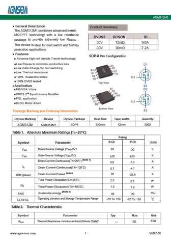
AGM312M1 General Description Product Summary The AGM312M1 combines advanced trench MOSFET technology with a low resistance BVDSS RDSON ID to provide extremely low R . package DS(ON) 30V 12m 9.0A This device is ideal for load switch and battery -30V 30m -7.2A protection applications. Features SOP-8 Pin Configuration Advance high cell density Trench technology Low
9.18. Size:905K cn agmsemi
agm310ap1.pdf 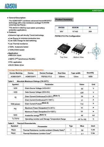
AGM310AP1 Fig.1 Power Dissipation Derating Curve Fig.2 Typical output Characteristics 1.2 50 1 V =10V GS 0.8 V =4.5V GS 25 0.6 0.4 0.2 0 0 0.5 1 1.5 2 0 Drain-Source voltage (V) 0 50 100 150 200 Temperature ( C) Fig.3 Threshold Voltage V.S Junction Temperature Fig.4 Resistance V.S Drain Current 2.5 20 2 1.5 10 1 0.5 0 0 -50 50 150 0 10 20 30 Junction Tempe
9.19. Size:2273K cn agmsemi
agm312me.pdf 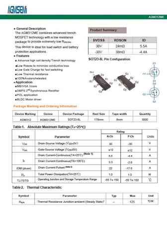
AGM312ME Table 3. N- Channel Electrical Characteristics (TJ=25 unless otherwise noted) Symbol Parameter Conditions Min Typ Max Unit On/Off States BV Drain-Source Breakdown Voltage V =0V I =250 A 30 -- -- V GS D DSS Zero Gate Voltage Drain Current V =30V,V =0V -- -- 1 A DS GS I DSS Gate-Body Leakage Current -- -- nA I V = 12V,V =0V GSS GS DS 100 V Gate Threshold Voltage
9.20. Size:887K cn agmsemi
agm312ap.pdf 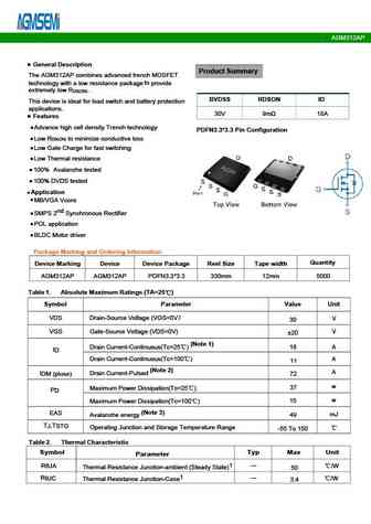
AGM312AP CHARACTERISTICS CURVES (TC = 25 C unless otherwise noted) Continuous Drain Current vs. TC Normalized RDS(ON) vs. TJ TJ, Junction Temperature ( C) TC, Case Temperature ( C) Normalized Vth vs. TJ Gate Charge Qg, Gate Charge (nC) TJ, Junction Temperature ( C) Normalized Transient Impedance Maximum Safe Operation Area VDS, Drain to Source Voltage (V) Square Wa
9.21. Size:1148K cn agmsemi
agm311mn.pdf 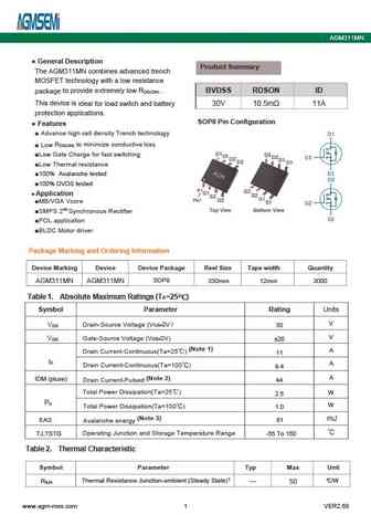
AGM311MN General Description Product Summary The AGM311MN combines advanced trench MOSFET technology with a low resistance to provide extremely low R . BVDSS RDSON ID package DS(ON) This device is ideal for load switch and battery 30V 10.5m 11A protection applications. SOP8 Pin Configuration Features Advance high cell density Trench technology R to minimize conductive
9.22. Size:754K cn agmsemi
agm315mn.pdf 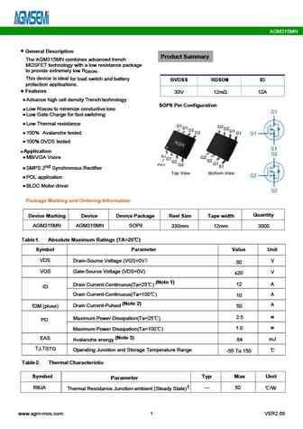
AGM315MN General Description Product Summary The AGM315MN combines advanced trench MOSFET technology with a low resistance package to provide extremely low R . DS(ON) This device is ideal for load switch and battery BVDSS RDSON ID protection applications. Features 30V 12m 12A Advance high cell density Trench technology SOP8 Pin Configuration Low R to minimize c
9.23. Size:854K cn agmsemi
agm318mbp.pdf 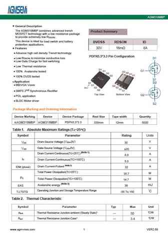
AGM318MBP General Description The AGM318MBP combines advanced trench Product Summary MOSFET technology with a low resistance package to provide extremely low R . DS(ON) This device is ideal for load switch and battery BVDSS RDSON ID protection applications. 30V 16m 8A Features Advance high cell density Trench technology PDFN3.3*3.3 Pin Configuration Low R to mi
Другие IGBT... AGM307MBP, AGM307MNQ, AGM312M1, AGM312M2, AGM312MAP, AGM312ME, AGM314MA, AGM314MAP, SPP20N60C3, AGM315MBP, AGM315MN, AGM318D, AGM318MAP, AGM318MBP, AGM318MN, AGM320M, AGM325ME
