AGM40P55A. Аналоги и основные параметры
Наименование производителя: AGM40P55A
Тип транзистора: MOSFET
Полярность: P
Предельные значения
Pd ⓘ
- Максимальная рассеиваемая мощность: 55 W
|Vds|ⓘ - Максимально допустимое напряжение сток-исток: 40 V
|Vgs|ⓘ - Максимально допустимое напряжение затвор-исток: 20 V
|Id| ⓘ - Максимально допустимый постоянный ток стока: 50 A
Tj ⓘ - Максимальная температура канала: 150 °C
Электрические характеристики
tr ⓘ -
Время нарастания: 31 ns
Cossⓘ - Выходная емкость: 282 pf
RDSonⓘ - Сопротивление сток-исток открытого транзистора: 0.013 Ohm
Тип корпуса: PDFN5X6
Аналог (замена) для AGM40P55A
- подборⓘ MOSFET транзистора по параметрам
AGM40P55A даташит
..1. Size:1567K cn agmsemi
agm40p55a.pdf 
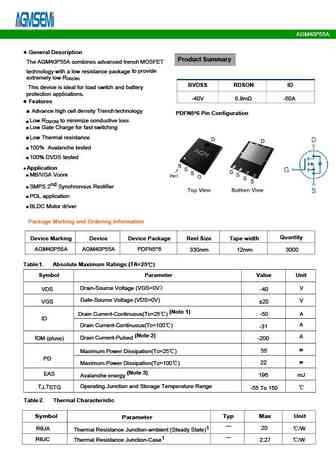
AGM40P55A Typical Characteristics 80 80 VGS = -10V VGS = -3.5V VDS= -5V VGS = -4.5V 60 60 40 40 VGS = -3V 20 20 VGS = -2.5V 0 0 0 Drain-source voltage -VDS 4 5 1 2 3 0 1 2 3 (V) Gate-source voltage -VGS (V) 4 Figure 1. Output Characteristics Figure 2. Transfer Characteristics 10 80 ID= -16A 60 40 1 20 0 0.1 0 3 6 9 12 0.2 0.4 0.6 0.8 1.0 1.2 Gate-sourc
0.1. Size:1323K cn agmsemi
agm40p55ap.pdf 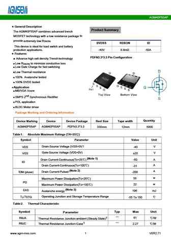
AGM40P55AP General Description Product Summary The AGM40P55AP combines advanced trench to MOSFET technology with a low resistance package provide extremely low R DS(ON) BVDSS RDSON ID This device is ideal for load switch and battery protection applications. -40V 8.9m -50A Features PDFN3.3*3.3 Pin Configuration Advance high cell density Trench technology Low R to min
6.1. Size:1406K cn agmsemi
agm40p55d.pdf 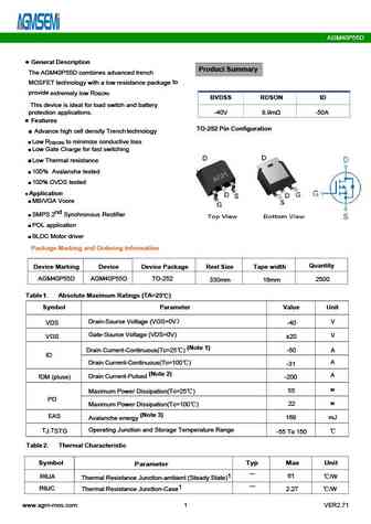
AGM40P55D General Description Product Summary The AGM40P55D combines advanced trench to MOSFET technology with a low resistance package provide extremely low R DS(ON) BVDSS RDSON ID This device is ideal for load switch and battery protection applications. -40V 8.9m -50A Features TO-252 Pin Configuration Advance high cell density Trench technology Low R to minimize c
8.1. Size:1269K cn agmsemi
agm40p25a.pdf 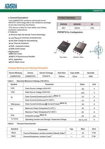
AGM40P25A Table 2. P-Channel Electrical Characteristics (TJ=25 unless otherwisenoted) Symbol Parameter Conditions Min Typ Max Unit On/Off States BVDSS Drain-Source Breakdown Voltage VGS=0V ID=-250 A -40 -- -- V Zero Gate Voltage Drain Current V =-40V,V =0V -1 DS GS I -- -- A DSS Gate-Body Leakage Current V = 20V,V =0V 100 GS DS I -- -- nA GSS V Gate Threshold Voltage V =V
8.2. Size:1056K cn agmsemi
agm40p30d.pdf 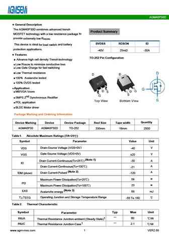
AGM40P30D General Description The AGM40P30D combines advanced trench Product Summary to MOSFET technology with a low resistance package provide extremely low R DS(ON) BVDSS RDSON ID This device is ideal and battery for load switch protection applications. -40V 25m -30A Features TO-252 Pin Configuration Advance high cell density Trench technology Low R to minimize
8.3. Size:527K cn agmsemi
agm40p35a.pdf 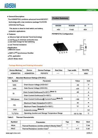
AGM40P35A General Description Product Summary The AGM40P35A combines advanced trench MOSFET to provide technology with a low resistance package extremely low R DS(ON) BVDSS RDSON ID This device is ideal and battery for load switch -40V 11m -60A protection applications. PDFN5*6 Pin Configuration Features Advance high cell density Trench technology Low R to minimize
8.4. Size:1016K cn agmsemi
agm40p100h.pdf 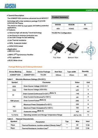
AGM40P100H Table 3. Electrical Characteristics (TJ=25 unless otherwise noted) Symbol Parameter Conditions Min Typ Max Unit On/Off States BVDSS Drain-Source Breakdown Voltage V =0V I =-250 A -40 -- -- V GS D Zero Gate Voltage Drain Current V =-40V,V =0V -- -- -1 A DS GS I DSS Gate-Body Leakage Current V = 20V,V =0V -- -- 100 nA GS DS I GSS VGS(th) Gate Threshold Voltage
8.5. Size:1520K cn agmsemi
agm40p26e.pdf 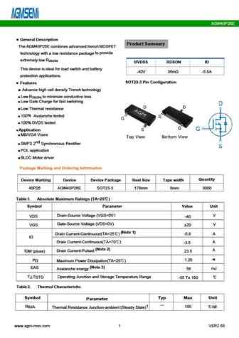
AGM40P26E General Description Product Summary The AGM40P26E combines advanced trench MOSFET to provide technology with a low resistance package extremely low R DS(ON) BVDSS RDSON ID This device is ideal and battery for load switch -40V 36m -5.8A protection applications. SOT23-3 Pin Configuration Features Advance high cell density Trench technology Low R to minimize
8.6. Size:879K cn agmsemi
agm40p13s.pdf 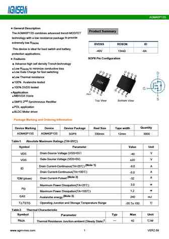
AGM40P13S General Description Product Summary The AGM40P13S combines advanced trench MOSFET to provide technology with a low resistance package extremely low R DS(ON) BVDSS RDSON ID This device is ideal and battery for load switch -40V 13m -8A protection applications. SOP8 Pin Configuration Features Advance high cell density Trench technology Low R to minimize cond
8.7. Size:1157K cn agmsemi
agm40p65ap.pdf 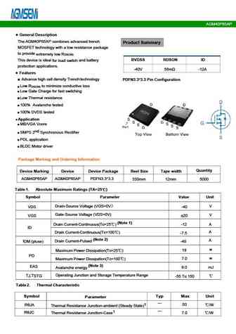
AGM40P65AP Typical Characteristics -VDS, - Drain -Source Voltage (V) Tj - Junction Temperature ( C) Fig1. Typical Output Characteristics Fig2. -V Gate -Source Voltage Vs. Tj GS(TH) -VGS, -Gate -Source Voltage (V) Tj - Junction Temperature ( C) Fig3. Typical Transfer Characteristics Fig4. Normalized On-Resistance Vs. Tj -VSD, -Source-Drain Voltage (V) -VDS, -Drain -Source Voltage (V)
8.8. Size:984K cn agmsemi
agm40p30ap.pdf 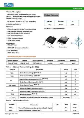
AGM40P30AP General Description The AGM40P30AP combines advanced trench Product Summary to MOSFET technology with a low resistance package provide extremely low R DS(ON) BVDSS RDSON ID This device is ideal and battery for load switch protection applications. -40V 26m -33A Features PDFN3.3*3.3 Pin Configuration Advance high cell density Trench technology Low R to mi
8.9. Size:1612K cn agmsemi
agm40p26ap.pdf 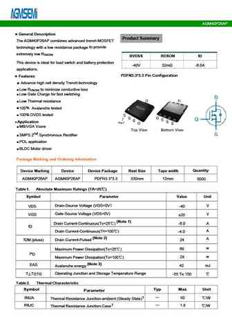
AGM40P26AP Table 3. Electrical Characteristics (TJ=25 unless otherwise noted) Symbol Parameter Conditions Min Typ Max Unit On/Off States BVDSS Drain-Source Breakdown Voltage V =0V I =-250 A -40 -- -- V GS D Zero Gate Voltage Drain Current V =-40V,V =0V -- -- -1 A DS GS I DSS Gate-Body Leakage Current V = 20V,V =0V -- -- 100 nA GS DS I GSS VGS(th) Gate Threshold Voltage
8.10. Size:646K cn agmsemi
agm40p65e.pdf 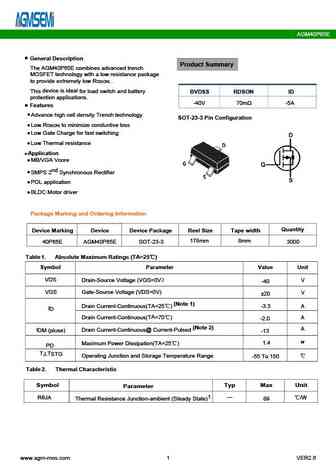
AGM40P65E General Description Product Summary The AGM40P65E combines advanced trench MOSFET technology with a low resistance package to provide extremely low R . DS(ON) device is ideal This for load switch and battery BVDSS RDSON ID protection applications. -40V 70m -5A Features Advance high cell density Trench technology SOT-23-3 Pin Configuration Low R to mi
8.11. Size:1616K cn agmsemi
agm40p75d.pdf 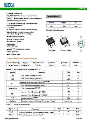
AGM40P75D General Description The AGM40P75D combines advanced trench Product Summary to MOSFET technology with a low resistance package provide extremely low R DS(ON) BVDSS RDSON ID This device is ideal for load switch and battery protection applications. -40V 7.0m -70A Features Advance high cell density Trench technology TO-252 Pin Configuration Low R to minimize
8.12. Size:963K cn agmsemi
agm40p35ap.pdf 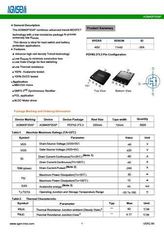
AGM40P35AP General Description Product Summary The AGM40P35AP combines advanced trench MOSFET to provide technology with a low resistance package extremely low R DS(ON) BVDSS RDSON ID This device is ideal for load switch and battery protection applications. -40V 11m -35A Features Advance high cell density Trench technology PDFN3.3*3.3 Pin Configuration Low R to mini
8.13. Size:1768K cn agmsemi
agm40p75a.pdf 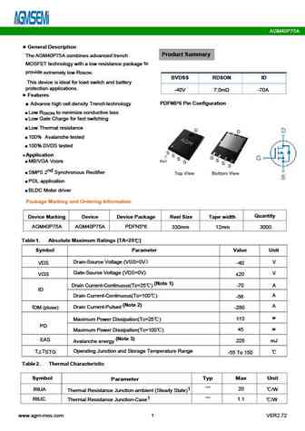
AGM40P75A General Description Product Summary The AGM40P75A combines advanced trench to MOSFET technology with a low resistance package provide extremely low R DS(ON) BVDSS RDSON ID This device is ideal for load switch and battery protection applications. -40V 7.0m -70A Features PDFN5*6 Pin Configuration Advance high cell density Trench technology Low R to minimize
8.14. Size:1189K cn agmsemi
agm40p150c.pdf 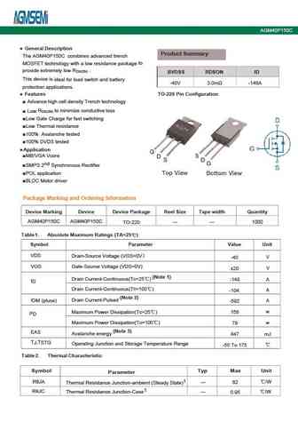
AGM40P150C Table 2. P-Channel Electrical Characteristics (TJ=25 unless otherwisenoted) Symbol Parameter Conditions Min Typ Max Unit On/Off States BVDSS Drain-Source Breakdown Voltage VGS=0V ID=-250 A -40 -- -- V Zero Gate Voltage Drain Current V =-40V,V =0V -1 DS GS I -- -- A DSS Gate-Body Leakage Current V = 40V,V =0V 100 GS DS I -- -- nA GSS V Gate Threshold Voltage V =
8.15. Size:1002K cn agmsemi
agm40p35d.pdf 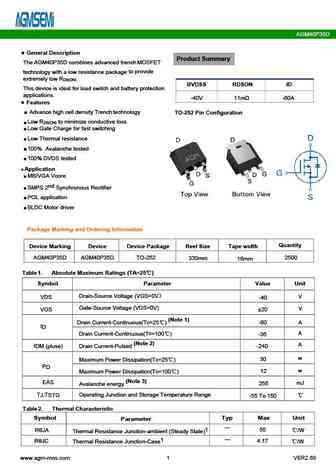
AGM40P35D General Description Product Summary The AGM40P35D combines advanced trench MOSFET to provide technology with a low resistance package extremely low R DS(ON) BVDSS RDSON ID This device is ideal for load switch and battery protection applications. -40V 11m -60A Features Advance high cell density Trench technology TO-252 Pin Configuration Low R to minimize co
8.16. Size:858K cn agmsemi
agm40p30a.pdf 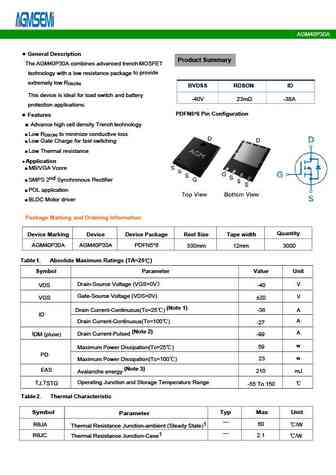
AGM40P30A Typical Characteristics -VDS,- Drain -Source Voltage (V) Tj - Junction Temperature ( C) Fig1. Typical Output Characteristics Fig2. -VGS(TH) Gate -Source Voltage Vs.Tj -VGS, -Gate -Source Voltage (V) Tj - Junction Temperature ( C) Fig3. Typical Transfer Characteristics Fig4. Normalized On-Resistance Vs. Tj -VSD, -Source-Drain Voltage (V) -VDS, -Drain -Source Voltage (V
8.17. Size:1241K cn agmsemi
agm40p100a.pdf 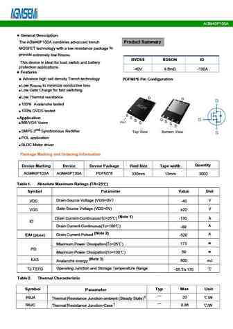
AGM40P100A Typical Electrical And Thermal Characteristics (Curves) Figure 1. Output Characteristics Figure 2. Transfer Characteristics Figure 3. Power Dissipation Figure 4. Drain Current Figure 5. BV vs Junction Temperature Figure 6. R vs Junction Temperature DSS DS(ON) www.agm-mos.com 3 VER2.69 AGM40P100A Figure 7. Gate Charge Waveforms Figure 8. Capacitance Figure 9. Body-
8.18. Size:1234K cn agmsemi
agm40p100c.pdf 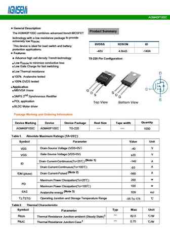
AGM40P100C Table 3. Electrical Characteristics (Tj=25 unless otherwise noted) Symbol Parameter Conditions Min Typ Max Unit On/Off States BVDSS Drain-Source Breakdown Voltage V =0V I =-250 A -40 -- -- V GS D Zero Gate Voltage Drain Current V =-40V,V =0V -- -- -1 A DS GS I DSS Gate-Body Leakage Current V = 20V,V =0V -- -- 100 nA GS DS I GSS VGS(th) Gate Threshold Voltage
8.19. Size:799K cn agmsemi
agm40p35a-ku.pdf 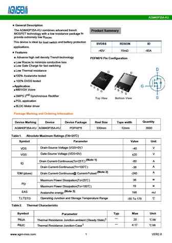
AGM40P35A-KU General Description The AGM40P35A-KU combines advanced trench Product Summary to MOSFET technology with a low resistance package provide extremely low R DS(ON) This device is ideal for load switch and battery protection BVDSS RDSON ID applications. -40V 15m -60A Features Advance high cell density Trench technology PDFN5*6 Pin Configuration Low R to min
8.20. Size:963K cn agmsemi
agm40p25ap.pdf 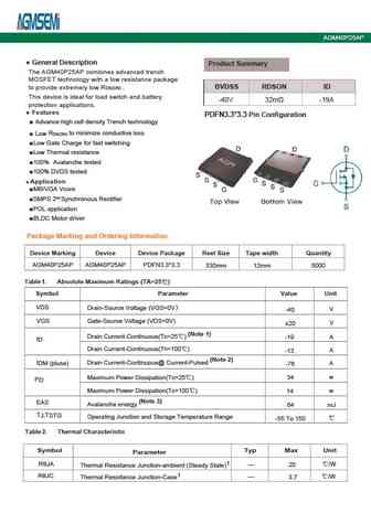
AGM40P25AP Typical Electrical And Thermal Characteristics (Curves) Figure 1. Output Characteristics Figure 2. Transfer Characteristics Figure 3. Power Dissipation Figure 4. Drain Current Figure 5. BV vs Junction Temperature Figure 6. R vs Junction Temperature DSS DS(ON) www.agm-mos.com 3 VER2.7 AGM40P25AP Typical Electrical And Thermal Characteristics (Curves) Figure 7. Gat
8.21. Size:1646K cn agmsemi
agm40p26s.pdf 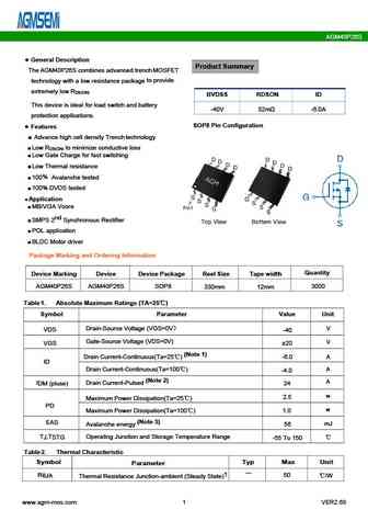
AGM40P26S General Description Product Summary The AGM40P26S combines advanced trench MOSFET to provide technology with a low resistance package extremely low R DS(ON) BVDSS RDSON ID This device is ideal and battery for load switch -40V 32m -6.0A protection applications. SOP8 Pin Configuration Features Advance high cell density Trench technology Low R to minimize co
Другие IGBT... AGM60P20R, AGM40P30A, AGM40P30AP, AGM40P30D, AGM40P35A, AGM40P35A-KU, AGM40P35AP, AGM40P35D, IRF540N, AGM40P55AP, AGM40P55D, AGM40P65AP, AGM40P65E, AGM40P75A, AGM40P75D, AGM602C, AGM6035A
