Скачать даташит для ced3423_ceu3423:
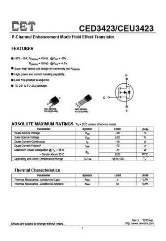
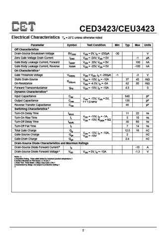
CED3423/CEU3423 P-Channel Enhancement Mode Field Effect Transistor FEATURES -30V, -18A, RDS(ON) = 45m @VGS = -10V. RDS(ON) = 80m @VGS = -4.5V. Super high dense cell design for extremely low RDS(ON). High power and current handing capability. D Lead free product is acquired. TO-251 & TO-252 package. D G G S CEU SERIES CED SERIES S TO-252(D-PAK) TO-251(I-PAK) ABSOLUTE MAXIMUM RATINGS Tc = 25 C unless otherwise noted Parameter Symbol Limit Units Drain-Source Voltage VDS -30 V Gate-Source Voltage VGS 20 V Drain Current-Continuous ID -18 A Drain Current-Pulsed a IDM -72 A Maximum Power Dissipation @ TC = 25 C 31 W PD - Derate above 25 C 0.25 W/ C Operating and Store Temperature Range TJ,Tstg -55 to 150 C Thermal Characteristics Parameter Symbol Limit Units Thermal Resistance, Junction-to-Case R JC 4 C/W Thermal Resistance, Junction-to-Ambient R JA
Ключевые слова - ALL TRANSISTORS DATASHEET
ced3423 ceu3423.pdf Проектирование, MOSFET, Мощность
ced3423 ceu3423.pdf Соответствует RoHS, Сервис, Симисторы, Полупроводник
ced3423 ceu3423.pdf База данных, Инновации, ИМС, Транзисторы
Параметры биполярного транзистора и их взаимосвязь

Список транзисторов
Обновления
BJT: ZDT6705 | GA1L4Z | GA1A4M | SBT42 | 2SA200-Y | 2SA200-O | 2SD882-Q | 2SD882-P | 2SD882-E | 2SC945-L | 2SC945-H | 2SC4226-R23 | 2SC3357-F | 2SC3357-E | 2SC3356-R26 | 2SC3356-R24 | 2SC3356-R23 | 2SB772-Q | 2SB772-P | 2SB772-E | 2SA1015-L
Popular searches
irfz44n | irf3205 | irfz44n datasheet | 2n4401 | bc547 transistor | bd139 | 2n4401 datasheet