Скачать даташит для ceh2331:
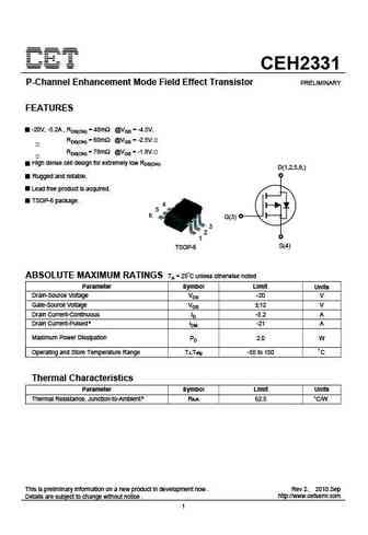
CEH2331 P-Channel Enhancement Mode Field Effect Transistor PRELIMINARY FEATURES -20V, -5.2A , RDS(ON) = 48m @VGS = -4.5V. RDS(ON) = 60m @VGS = -2.5V. RDS(ON) = 78m @VGS = -1.8V. High dense cell design for extremely low RDS(ON). D(1,2,5,6,) Rugged and reliable. Lead free product is acquired. TSOP-6 package. 4 5 6 G(3) 3 2 1 S(4) TSOP-6 ABSOLUTE MAXIMUM RATINGS TA = 25 C unless otherwise noted Parameter Symbol Limit Units Drain-Source Voltage VDS -20 V Gate-Source Voltage VGS 12 V Drain Current-Continuous ID -5.2 A Drain Current-Pulsed a IDM -21 A Maximum Power Dissipation PD 2.0 W Operating and Store Temperature Range TJ,Tstg -55 to 150 C Thermal Characteristics Parameter Symbol Limit Units Thermal Resistance, Junction-to-Ambient b R JA 62.5 C/W This is preliminary information on a new product in development now . Rev 2. 2010.Sep http /
Ключевые слова - ALL TRANSISTORS DATASHEET
ceh2331.pdf Проектирование, MOSFET, Мощность
ceh2331.pdf Соответствует RoHS, Сервис, Симисторы, Полупроводник
ceh2331.pdf База данных, Инновации, ИМС, Транзисторы
Параметры биполярного транзистора и их взаимосвязь

Список транзисторов
Обновления
BJT: ZDT6705 | GA1L4Z | GA1A4M | SBT42 | 2SA200-Y | 2SA200-O | 2SD882-Q | 2SD882-P | 2SD882-E | 2SC945-L | 2SC945-H | 2SC4226-R23 | 2SC3357-F | 2SC3357-E | 2SC3356-R26 | 2SC3356-R24 | 2SC3356-R23 | 2SB772-Q | 2SB772-P | 2SB772-E | 2SA1015-L
Popular searches
irfz44n | irf3205 | irfz44n datasheet | 2n4401 | bc547 transistor | bd139 | 2n4401 datasheet