2SD2066
- Даташиты. Аналоги. Основные параметры
Наименование производителя: 2SD2066
Тип материала: Si
Полярность: NPN
Максимальная рассеиваемая мощность (Pc): 120
W
Макcимально допустимое напряжение коллектор-база (Ucb): 160
V
Макcимальный постоянный ток коллектора (Ic): 12
A
Предельная температура PN-перехода (Tj): 150
°C
Статический коэффициент передачи тока (hfe): 30
Корпус транзистора:
TO218
Аналоги (замена) для 2SD2066
2SD2066
Datasheet (PDF)
..1. Size:199K inchange semiconductor
2sd2066.pdf 
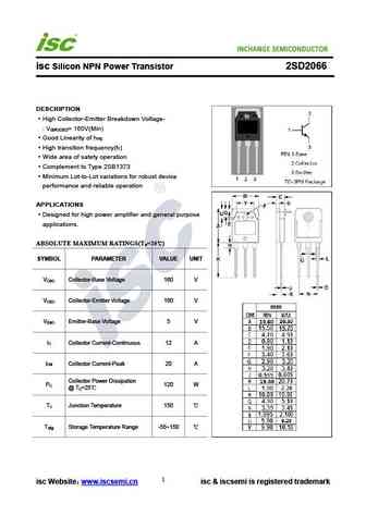
INCHANGE Semiconductor isc Silicon NPN Power Transistor 2SD2066 DESCRIPTION High Collector-Emitter Breakdown Voltage- V = 160V(Min) (BR)CEO Good Linearity of h FE High transition frequency(f ) T Wide area of satety operation Complement to Type 2SB1373 Minimum Lot-to-Lot variations for robust device performance and reliable operation APPLICATIONS Designed for high
8.1. Size:39K rohm
2sd2061.pdf 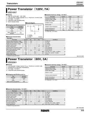
2SD1957 Transistors Transistors 2SD2061 (94L-919 D301) (94L-1016-D304) 315
8.2. Size:54K panasonic
2sd2067.pdf 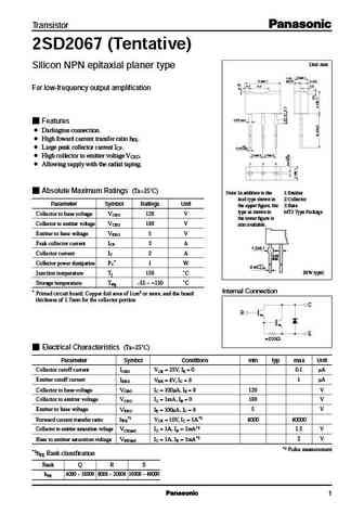
Transistor 2SD2067 (Tentative) Unit mm Silicon NPN epitaxial planer type 2.5 0.1 1.05 6.9 0.1 0.05 (1.45) 0.7 4.0 0.8 For low-frequency output amplification 0.65 max. Features Darlington connection. High foward current transfer ratio hFE. +0.1 Large peak collector current ICP. 0.45 0.05 2.5 0.5 2.5 0.5 High collector to emitter voltage VCEO. 1 2 3 Allowing supp
8.3. Size:51K panasonic
2sd2064.pdf 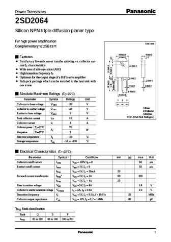
Power Transistors 2SD2064 Silicon NPN triple diffusion planar type For high power amplification Unit mm Complementary to 2SB1371 15.0 0.3 5.0 0.2 Features 11.0 0.2 3.2 Satisfactory foward current transfer ratio hFE vs. collector cur- rent IC characteristics 3.2 0.1 Wide area of safe operation (ASO) High transition frequency fT Optimum for the output stage of a HiFi aud
8.4. Size:59K panasonic
2sd2067 e.pdf 
Transistor 2SD2067 (Tentative) Unit mm Silicon NPN epitaxial planer type 2.5 0.1 1.05 6.9 0.1 0.05 (1.45) 0.7 4.0 0.8 For low-frequency output amplification 0.65 max. Features Darlington connection. High foward current transfer ratio hFE. +0.1 Large peak collector current ICP. 0.45 0.05 2.5 0.5 2.5 0.5 High collector to emitter voltage VCEO. 1 2 3 Allowing supp
8.5. Size:616K jiangsu
2sd2061.pdf 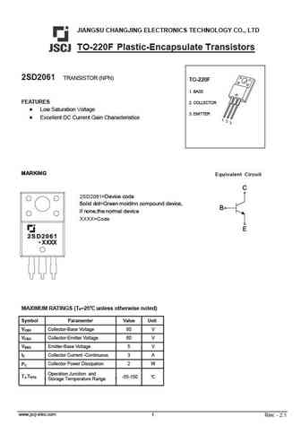
JIANGSU CHANGJING ELECTRONICS TECHNOLOGY CO., LTD TO-220F Plastic-Encapsulate Transistors 2SD2061 TRANSISTOR (NPN) TO-220F 1. BASE FEATURES 2. COLLECTOR Low Saturation Voltage 3. EMITTER Excellent DC Current Gain Characteristice 1 2 3 Equivalent Circuit 2SD2061=Device code Solid dot=Green moldinn compound device, if none,the normal device XXXX=Code 2SD206
8.6. Size:46K jmnic
2sd2060.pdf 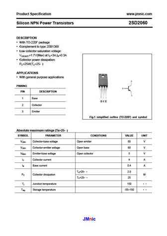
Product Specification www.jmnic.com Silicon NPN Power Transistors 2SD2060 DESCRIPTION With TO-220F package Complement to type 2SB1368 Low collector saturation voltage VCE(SAT)=1.7V(Max) at IC=3A,IB=0.3A Collector power dissipation PC=25W(TC=25 ) APPLICATIONS With general purpose applications PINNING PIN DESCRIPTION 1 Base 2 Collector 3 Emitter Fig.1 si
8.7. Size:108K jmnic
2sd2061.pdf 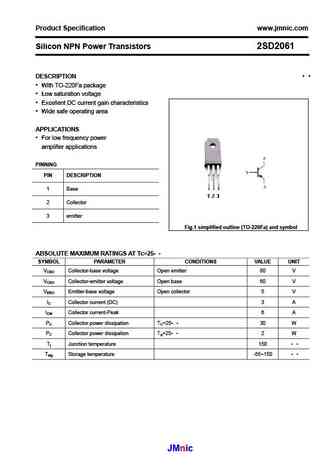
Product Specification www.jmnic.com Silicon NPN Power Transistors 2SD2061 DESCRIPTION With TO-220Fa package Low saturation voltage Excellent DC current gain characteristics Wide safe operating area APPLICATIONS For low frequency power amplifier applications PINNING PIN DESCRIPTION 1 Base 2 Collector 3 emitter Fig.1 simplified outline (TO-220Fa) and symbol
8.8. Size:217K lge
2sd2061 2sd2061 to-220.pdf 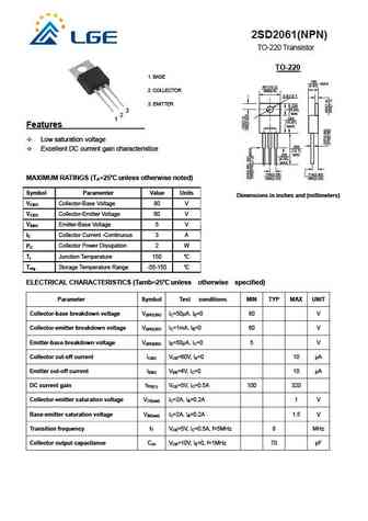
2SD2061(NPN) TO-220 Transistor TO-220 1. BASE 2. COLLECTOR 3. EMITTER 3 2 1 Features Low saturation voltage Excellent DC current gain characteristice MAXIMUM RATINGS (TA=25 unless otherwise noted) Symbol Paramenter Value Units Dimensions in inches and (millimeters) VCBO Collector-Base Voltage 80 V VCEO Collector-Emitter Voltage 60 V VEBO Emitter-Base Voltage
8.9. Size:199K inchange semiconductor
2sd2060.pdf 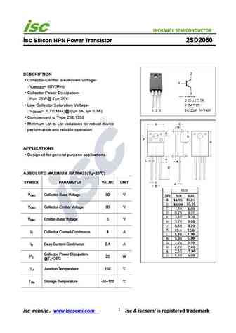
isc Silicon NPN Power Transistor 2SD2060 DESCRIPTION Collector-Emitter Breakdown Voltage- V = 80V(Min) (BR)CEO Collector Power Dissipation- P = 25W@ T = 25 C C Low Collector Saturation Voltage- V = 1.7V(Max)@ (I = 3A, I = 0.3A) CE(sat) C B Complement to Type 2SB1368 Minimum Lot-to-Lot variations for robust device performance and reliable operation APPLICATIONS
8.10. Size:195K inchange semiconductor
2sd2061.pdf 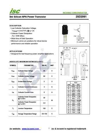
isc Silicon NPN Power Transistor 2SD2061 DESCRIPTION Low Collector Saturation Voltage V = 0.3V(TYP.) @ I = 2A CE(sat) C Collector Power Dissipation P = 30W (Max) C Wide Area of Safe Operation Minimum Lot-to-Lot variations for robust device performance and reliable operation APPLICATIONS Designed for low frequency power amplifier applications ABSOLUTE MAXIMUM RATINGS(T
8.11. Size:181K inchange semiconductor
2sd2062.pdf 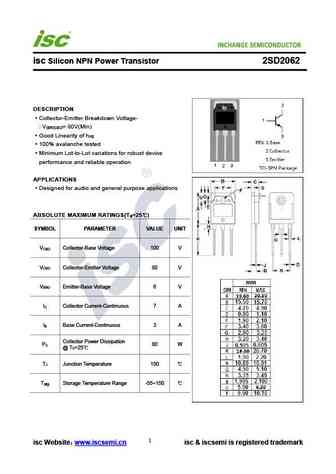
INCHANGE Semiconductor isc Silicon NPN Power Transistor 2SD2062 DESCRIPTION Collector-Emitter Breakdown Voltage- V = 80V(Min) (BR)CEO Good Linearity of h FE 100% avalanche tested Minimum Lot-to-Lot variations for robust device performance and reliable operation APPLICATIONS Designed for audio and general purpose applications ABSOLUTE MAXIMUM RATINGS(T =25 ) a SYMBOL
8.12. Size:199K inchange semiconductor
2sd2065.pdf 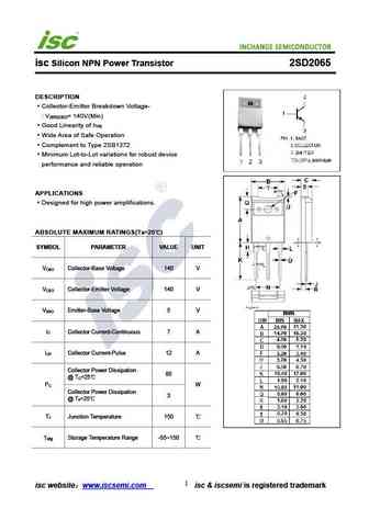
isc Silicon NPN Power Transistor 2SD2065 DESCRIPTION Collector-Emitter Breakdown Voltage- V = 140V(Min) (BR)CEO Good Linearity of h FE Wide Area of Safe Operation Complement to Type 2SB1372 Minimum Lot-to-Lot variations for robust device performance and reliable operation APPLICATIONS Designed for high power amplifications. ABSOLUTE MAXIMUM RATINGS(T =25 ) a SYMBO
Другие транзисторы... 2SD2059
, 2SD206
, 2SD2060
, 2SD2061
, 2SD2062
, 2SD2063
, 2SD2064
, 2SD2065
, BD140
, 2SD2067
, 2SD2068
, 2SD206A
, 2SD207
, 2SD2070
, 2SD2071
, 2SD2072
, 2SD2073
.
History: MJE13004D
| 40294

