413 datasheet, аналоги, основные параметры
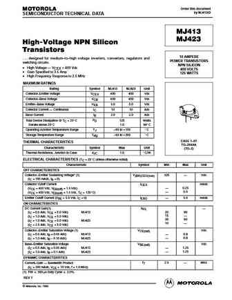
Наименование производителя: 413
Тип материала: Si
Полярность: NPN
Предельные значения
Максимальная рассеиваемая мощность (Pc): 125 W
Макcимально допустимое напряжение коллектор-база (Ucb): 400 V
Макcимально допустимое напряжение коллектор-эмиттер (Uce): 325 V
Макcимально допустимое напряжение эмиттер-база (Ueb): 5 V
Макcимальный постоянный ток коллектора (Ic): 7 A
Предельная температура PN-перехода (Tj): 150 °C
Электрические характеристики
Граничная частота коэффициента передачи тока (ft): 4 MHz
Статический коэффициент передачи тока (hFE): 10
Корпус транзистора: TO3
Аналоги (замена) для 413
- подборⓘ биполярного транзистора по параметрам
413 даташит
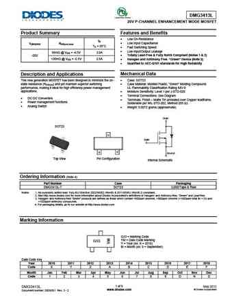
ao3413l.pdf
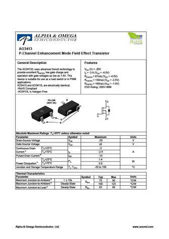
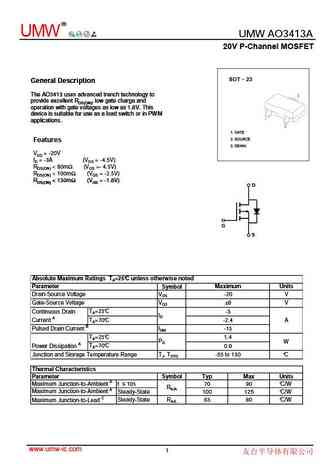
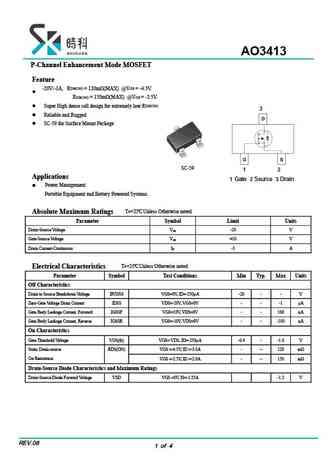
AO3413 P-Channel Enhancement Mode Field Effect Transistor General Description Features The AO3413/L uses advanced trench technology to VDS (V) = -20V provide excellent RDS(ON), low gate charge and ID = -3 A (VGS = -4.5V) operation with gate voltages as low as 1.8V. This RDS(ON)
2sk2413.pdf
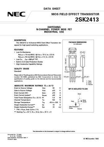
DATA SHEET MOS FIELD EFFECT TRANSISTOR 2SK2413 SWITCHING N-CHANNEL POWER MOS FET INDUSTRIAL USE DESCRIPTION PACKAGE DIMENSIONS The 2SK2413 is N-Channel MOS Field Effect Transistor de- (in millimeter) signed for high speed switching applications. FEATURES 4.5 0.2 Low On-Resistance 8.0 0.2 RDS(on)1 = 70 m MAX. (@ VGS = 10 V, ID = 5.0 A) RDS(on)2 = 95 m MAX. (@ VGS =
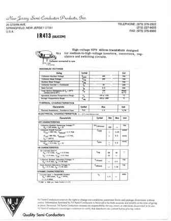
mj413rev.pdf
Order this document MOTOROLA by MJ413/D SEMICONDUCTOR TECHNICAL DATA MJ413 MJ423 High-Voltage NPN Silicon Transistors 10 AMPERE . . . designed for medium to high voltage inverters, converters, regulators and POWER TRANSISTORS switching circuits. NPN SILICON High Voltage VCEX = 400 Vdc 400 VOLTS Gain Specified to 3.
irf7413.pdf
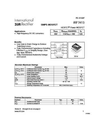
PD- 91330F IRF7413 SMPS MOSFET HEXFET Power MOSFET VDSS RDS(on) max(mW) ID Applications l High frequency DC-DC converters 30V 11@VGS = 10V 12A Benefits A A l Low Gate to Drain Charge to Reduce 1 8 S D Switching Losses 2 7 S D l Fully Characterized Capacitance Including 3 6 S Effective COSS to Simplify Design, (See D App. Note AN1001) 4 5 G D l Fully Characterized Avalan
irf7413pbf.pdf
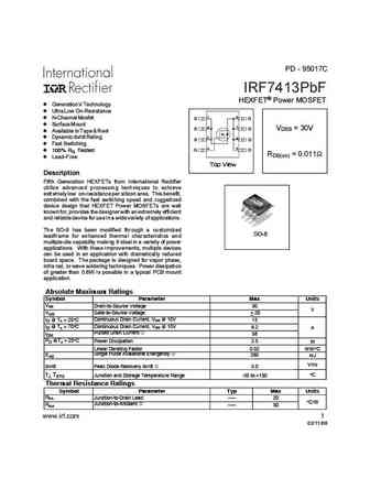
PD - 95017C IRF7413PbF HEXFET Power MOSFET l Generation V Technology l Ultra Low On-Resistance A A 1 8 l N-Channel Mosfet S D l Surface Mount 2 7 S D VDSS = 30V l Available in Tape & Reel l Dynamic dv/dt Rating 3 6 S D l Fast Switching 4 5 G D l 100% RG Tested RDS(on) = 0.011 l Lead-Free Top View Description Fifth Generation HEXFETs from International Rectifier util
irf7413qpbf.pdf
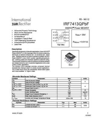
PD - 96112 IRF7413QPbF HEXFET Power MOSFET A l Advanced Process Technology A 1 8 S D l Ultra Low On-Resistance 2 7 l N Channel MOSFET S D VDSS = 30V l Surface Mount 3 6 S D l Available in Tape & Reel 4 5 l 150 C Operating Temperature G D RDS(on) = 0.011 l Automotive [Q101] Qualified l Lead-Free Top View Description Specifically designed for Automotive applications,
irf7413zpbf.pdf
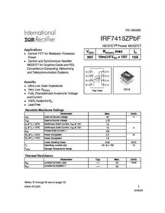
PD - 95335D IRF7413ZPbF HEXFET Power MOSFET Applications VDSS RDS(on) max ID l Control FET for Notebook Processor 10m @VGS = 10V Power 30V 13A l Control and Synchronous Rectifier MOSFET for Graphics Cards and POL A Converters in Computing, Networking A 1 8 S D and Telecommunication Systems 2 7 S D 3 6 S D Benefits 4 5 G D l Ultra-Low Gate Impedance SO-8 l Very Low RDS
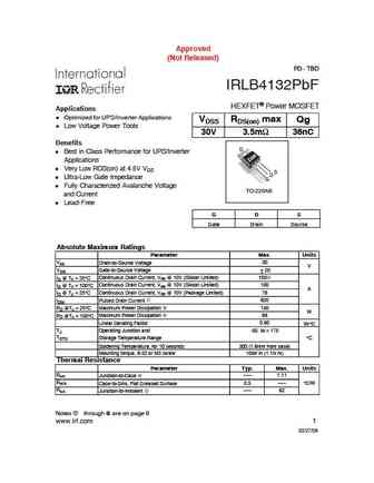
irlb4132pbf.pdf
Approved (Not Released) PD - TBD IRLB4132PbF HEXFET Power MOSFET Applications l Optimized for UPS/Inverter Applications VDSS RDS(on) max Qg l Low Voltage Power Tools 30V 3.5m 36nC Benefits D l Best in Class Performance for UPS/Inverter Applications l Very Low RDS(on) at 4.5V VGS S D l Ultra-Low Gate Impedance G l Fully Characterized Avalanche Voltage TO-220AB and Curr
irl5y7413cm.pdf
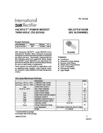
PD - 94164A HEXFET POWER MOSFET IRL5Y7413CM THRU-HOLE (TO-257AA) 30V, N-CHANNEL Product Summary Part Number BVDSS RDS(on) ID IRL5Y7413CM 30V 0.025 18A* Fifth Generation HEXFET power MOSFETs from TO-257AA International Rectifier utilize advanced processing techniques to achieve the lowest possible on-resistance per silicon unit area. This benefit, combined with the Features
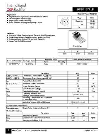
irfb4137pbf.pdf
IRFB4137PbF HEXFET Power MOSFET Application High Efficiency Synchronous Rectification in SMPS D VDSS 300V Uninterruptible Power Supply High Speed Power Switching RDS(on) typ. 56m Hard Switched and High Frequency Circuits G 69m max S ID 38A Benefits Improved Gate, Avalanche and Dynamic dV/dt Ruggedness Fully Chara
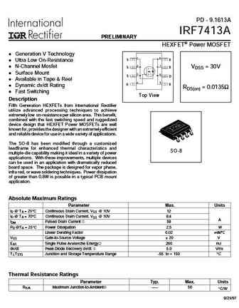
irf7413a.pdf
PD - 9.1613A IRF7413A PRELIMINARY HEXFET Power MOSFET A Generation V Technology A 1 8 S D Ultra Low On-Resistance 2 7 N-Channel Mosfet VDSS = 30V S D Surface Mount 3 6 S D Available in Tape & Reel 4 5 G D Dynamic dv/dt Rating RDS(on) = 0.0135 Fast Switching Top View Description Fifth Generation HEXFETs from International Rectifier utilize advanced processing
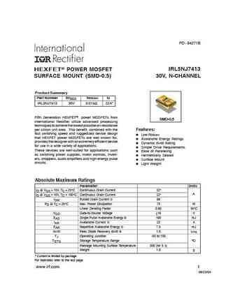
irl5nj7413.pdf
PD - 94271B IRL5NJ7413 HEXFET POWER MOSFET SURFACE MOUNT (SMD-0.5) 30V, N-CHANNEL Product Summary Part Number BVDSS RDS(on) ID IRL5NJ7413 30V 0.014 22A* Fifth Generation HEXFET power MOSFETs from SMD-0.5 International Rectifier utilize advanced processing techniques to achieve the lowest possible on-resistance per silicon unit area. This benefit, combined with the Features
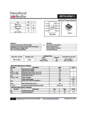
irf7413pbf-1.pdf
IRF7413PbF-1 HEXFET Power MOSFET A VDS 30 V A 1 8 S D RDS(on) max 0.011 2 7 S D (@V = 10V) GS 3 6 Qg (typical) 52 nC S D ID 4 5 G D 13 A (@T = 25 C) A SO-8 Top View Features Benefits Industry-standard pinout SO-8 Package Multi-Vendor Compatibility Compatible with Existing Surface Mount Techniques Easier Manufacturing RoHS Compliant, Halogen-Free Environme
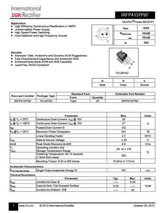
irfp4137pbf.pdf
IRFP4137PbF HEXFET Power MOSFET Application High Efficiency Synchronous Rectification in SMPS D VDSS 300V Uninterruptible Power Supply High Speed Power Switching RDS(on) typ. 56m Hard Switched and High Frequency Circuits G 69m max S ID 38A Benefits Improved Gate, Avalanche and Dynamic dV/dt Ruggedness Fully Chara
irlb4132.pdf
Approved (Not Released) PD - TBD IRLB4132PbF HEXFET Power MOSFET Applications l Optimized for UPS/Inverter Applications VDSS RDS(on) max Qg l Low Voltage Power Tools 30V 3.5m 36nC Benefits D l Best in Class Performance for UPS/Inverter Applications l Very Low RDS(on) at 4.5V VGS S D l Ultra-Low Gate Impedance G l Fully Characterized Avalanche Voltage TO-220AB and Curr
irf7413gpbf.pdf
PD - 96250 IRF7413GPbF HEXFET Power MOSFET l Generation V Technology l Ultra Low On-Resistance A A 1 8 l N-Channel Mosfet S D l Surface Mount 2 7 S D VDSS = 30V l Available in Tape & Reel l Dynamic dv/dt Rating 3 6 S D l Fast Switching 4 5 G D l 100% RG Tested RDS(on) = 0.011 l Lead-Free l Halogen-Free Top View Description Fifth Generation HEXFETs from International
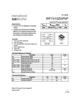
irf7413zgpbf.pdf
PD - 96249 IRF7413ZGPbF HEXFET Power MOSFET Applications VDSS RDS(on) max ID l Control FET for Notebook Processor 10m @VGS = 10V Power 30V 13A l Control and Synchronous Rectifier MOSFET for Graphics Cards and POL A Converters in Computing, Networking A 1 8 S D and Telecommunication Systems 2 7 S D 3 6 S D Benefits 4 5 l Ultra-Low Gate Impedance G D l Very Low RDS(on)
pbss4130t.pdf
DISCRETE SEMICONDUCTORS DATA SHEET M3D088 PBSS4130T 30 V, 1 A NPN low VCEsat (BISS) transistor Product specification 2003 Nov 27 Philips Semiconductors Product specification 30 V, 1 A PBSS4130T NPN low VCEsat (BISS) transistor FEATURES QUICK REFERENCE DATA Low collector-emitter saturation voltage VCEsat SYMBOL PARAMETER MAX. UNIT High collector current capability IC and I
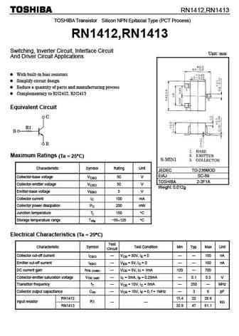
rn1412 rn1413.pdf
RN1412,RN1413 TOSHIBA Transistor Silicon NPN Epitaxial Type (PCT Process) RN1412,RN1413 Switching, Inverter Circuit, Interface Circuit Unit mm And Driver Circuit Applications With built-in bias resistors Simplify circuit design Reduce a quantity of parts and manufacturing process Complementary to RN2412, RN2413 Equivalent Circuit Maximum Ratings (Ta = 25 C)
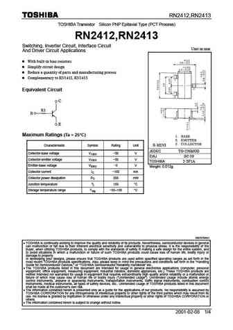
rn2412-rn2413.pdf
RN2412,RN2413 TOSHIBA Transistor Silicon PNP Epitaxial Type (PCT Process) RN2412,RN2413 Switching, Inverter Circuit, Interface Circuit Unit in mm And Driver Circuit Applications With built-in bias resistors Simplify circuit design Reduce a quantity of parts and manufacturing process Complementary to RN1412, RN1413 Equivalent Circuit Maximum Ratings (Ta = 25 C) Ch
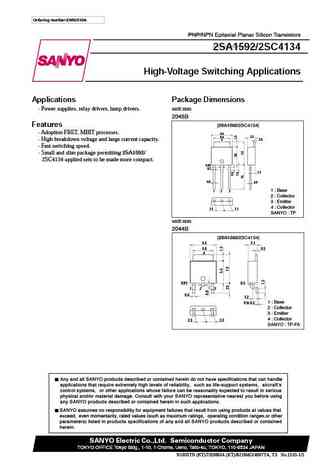
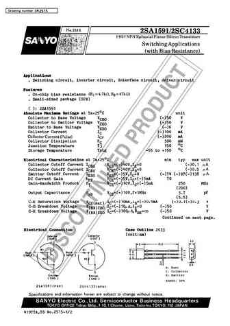
2sc4134.pdf
Ordering number ENN2510A PNP/NPN Epitaxial Planar Silicon Transistors 2SA1592/2SC4134 High-Voltage Switching Applications Applications Package Dimensions Power supplies, relay drivers, lamp drivers. unit mm 2045B Features [2SA1592/2SC4134] Adoption FBET, MBIT processes. 6.5 2.3 5.0 High breakdown voltage and large current capacity. 0.5 4 Fast switching speed.
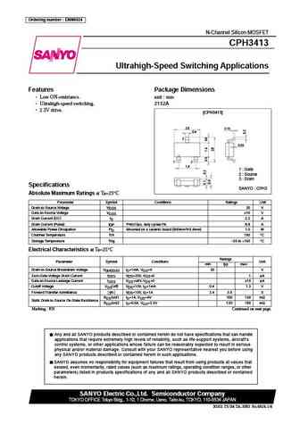
cph3413.pdf
Ordering number ENN6924 CPH3413 N-Channel Silicon MOSFET CPH3413 Ultrahigh-Speed Switching Applications Features Package Dimensions Low ON-resistance. unit mm Ultrahigh-speed switching. 2152A 2.5V drive. [CPH3413] 2.9 0.15 0.4 3 0.05 1 2 1.9 1 Gate 2 Source 3 Drain Specifications SANYO CPH3 Absolute Maximum Ratings at Ta=25 C Parameter Symbol Cond
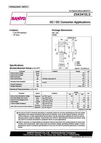
2sk3413ls.pdf
Ordering number ENN7151 2SK3413LS N-Channel Silicon MOSFET 2SK3413LS DC / DC Converter Applications Features Package Dimensions Low ON-resistance. unit mm 4V drive. 2078C [2SK3413LS] 10.0 4.5 3.2 2.8 0.9 1.2 1.2 0.75 0.7 1 2 3 1 Gate 2 Drain 3 Source Specifications 2.55 2.55 Absolute Maximum Ratings at Ta=25 C SANYO TO-220FI(LS) Parameter Symbol Condi
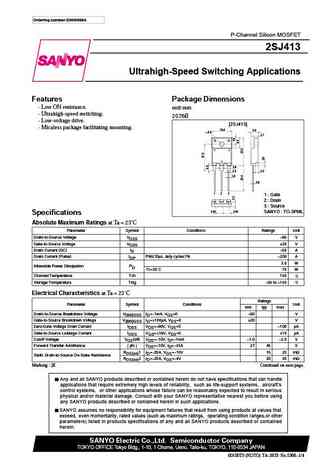
2sj413.pdf
Ordering number ENN5366A P-Channel Silicon MOSFET 2SJ413 Ultrahigh-Speed Switching Applications Features Package Dimensions Low ON resistance. unit mm Ultrahigh-speed switching. 2076B Low-voltage drive. [2SJ413] Micaless package facilitating mounting. 16.0 5.6 3.4 3.1 2.8 2.0 2.0 1.0 0.6 1 2 3 1 Gate 2 Drain 3 Source 5.45 5.45 SANYO TO-3PML Speci
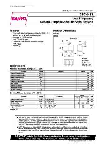
2sc4413.pdf
Ordering number EN2923 NPN Epitaxial Planar Silicon Transistor 2SC4413 Low-Frequency General-Purpose Amplifier Applications Features Package Dimensions Very small-sized package permitting the 2SC4413- unit mm applied sets to be made small and slim. 2059B Adoption of FBET process. [2SC4413] High DC current gain. 0.3 0.15 Low collector-to-emitter saturation voltage.
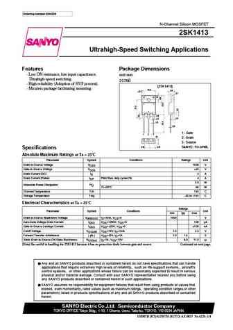
2sk1413.pdf
Ordering number EN4229 N-Channel Silicon MOSFET 2SK1413 Ultrahigh-Speed Switching Applications Features Package Dimensions Low ON resistance, low input capacitance, unit mm Ultrahigh-speed switching. 2076B High reliability (Adoption of HVP process). [2SK1413] Micaless package facilitating mounting. 16.0 5.6 3.4 3.1 2.8 2.0 2.0 1.0 0.6 1 Gate 1 2 3 2 Drain
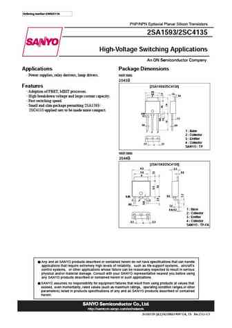
2sa1593 2sc4135.pdf
Ordering number ENN2511A PNP/NPN Epitaxial Planar Silicon Transistors 2SA1593/2SC4135 High-Voltage Switching Applications Applications Package Dimensions Power supplies, relay derivers, lamp drivers. unit mm 2045B Features [2SA1593/2SC4135] Adoption of FBET, MBIT processes. 6.5 2.3 5.0 0.5 High breakdown voltage and large current capacity. 4 Fast switching speed.
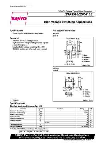
2sc4135.pdf
Ordering number EN2511A PNP/NPN Epitaxial Planar Silicon Transistors 2SA1593/2SC4135 High-Voltage Switching Applications Applications Package Dimensions Power supplies, relay derivers, lamp drivers. unit mm 2045B Features [2SA1593/2SC4135] Adoption of FBET, MBIT processes. High breakdown voltage and large current capacity. Fast switching speed. Small and slim pack
rej03g0413 h5n2515p.pdf
To our customers, Old Company Name in Catalogs and Other Documents On April 1st, 2010, NEC Electronics Corporation merged with Renesas Technology Corporation, and Renesas Electronics Corporation took over all the business of both companies. Therefore, although the old company name remains in this document, it is a valid Renesas Electronics document. We appreciate your understanding.
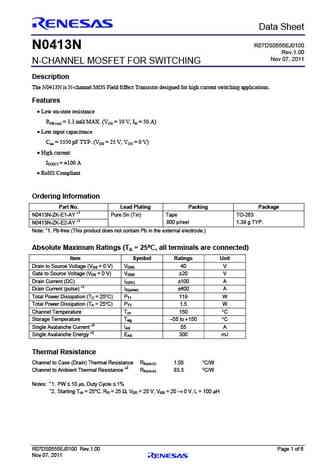
n0413n.pdf
Preliminary Data Sheet R07DS0555EJ0100 N0413N Rev.1.00 Nov 07, 2011 N-CHANNEL MOSFET FOR SWITCHING Description The N0413N is N-channel MOS Field Effect Transistor designed for high current switching applications. Features Low on-state resistance RDS (on) = 3.3 m MAX. (VGS = 10 V, ID = 50 A) Low input capacitance Ciss = 5550 pF TYP. (VDS = 25 V, VGS = 0 V) H
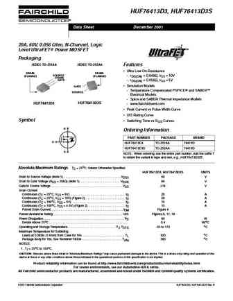
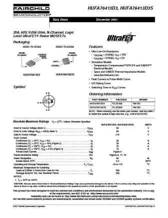
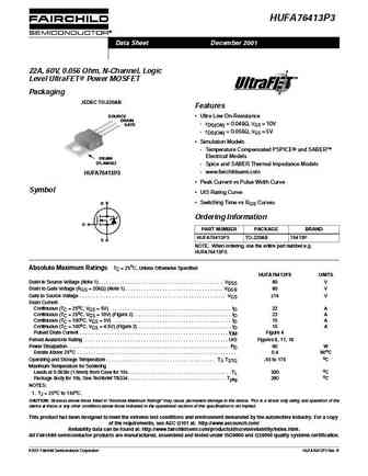
hufa76413d3 hufa76413d3s.pdf
HUFA76413D3, HUFA76413D3S Data Sheet December 2001 20A, 60V, 0.056 Ohm, N-Channel, Logic Level UltraFET Power MOSFETs Packaging JEDEC TO-251AA JEDEC TO-252AA Features Ultra Low On-Resistance DRAIN DRAIN SOURCE - rDS(ON) = 0.049 , VGS = 10V (FLANGE) (FLANGE) DRAIN GATE - rDS(ON) = 0.056 , VGS = 5V GATE Simulation Models SOURCE - Temperature Compensated PSPICE a
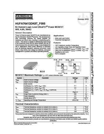
hufa76413dk8t f085.pdf
October 2010 HUFA76413DK8T_F085 N-Channel Logic Level UltraFET Power MOSFET 60V, 4.8A, 56m General Description These N-Channel power MOSFETs are manufactured us- Applications ing the innovative UltraFET process. This advanced pro- Motor and Load Control cess technology achieves the lowest possible on- resistance per silicon area, resulting in outstanding perfor- Powertr
huf76413dk f085.pdf
October 2010 HUFA76413DK8T_F085 N-Channel Logic Level UltraFET Power MOSFET 60V, 4.8A, 56m General Description These N-Channel power MOSFETs are manufactured us- Applications ing the innovative UltraFET process. This advanced pro- Motor and Load Control cess technology achieves the lowest possible on- resistance per silicon area, resulting in outstanding perfor- Powertr
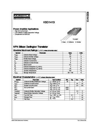
ksd1413.pdf
Power Amplifier Applications Power Amplifier Applications Power Amplifier Applications Power Amplifier Applications High DC Current Gain Low Collector- Emitter Saturation Voltage Complement to KSB1023 TO-220F 1. Base 2. Collector 3. Emitter NPN Silicon Darlington Transistor NPN Silicon Darlington Transistor NPN Silicon Darlingt
hufa76413p3.pdf
HUFA76413P3 Data Sheet December 2001 22A, 60V, 0.056 Ohm, N-Channel, Logic Level UltraFET Power MOSFET Packaging JEDEC TO-220AB Features SOURCE Ultra Low On-Resistance DRAIN - rDS(ON) = 0.049 , VGS = 10V GATE - rDS(ON) = 0.056 , VGS = 5V Simulation Models - Temperature Compensated PSPICE and SABER Electrical Models DRAIN (FLANGE) - Spice and SABER Thermal
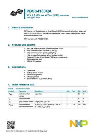
pbss4130qa.pdf
PBSS4130QA 30 V, 1 A NPN low VCEsat (BISS) transistor 28 August 2013 Product data sheet 1. General description NPN low VCEsat Breakthrough In Small Signal (BISS) transistor in a leadless ultra small DFN1010D-3 (SOT1215) Surface-Mounted Device (SMD) plastic package with visible and solderable side pads. PNP complement PBSS5130QA. 2. Features and benefits Very low collector-emitter
pbss4130t.pdf
Important notice Dear Customer, On 7 February 2017 the former NXP Standard Product business became a new company with the tradename Nexperia. Nexperia is an industry leading supplier of Discrete, Logic and PowerMOS semiconductors with its focus on the automotive, industrial, computing, consumer and wearable application markets In data sheets and application notes which still contain
pbss4130panp.pdf
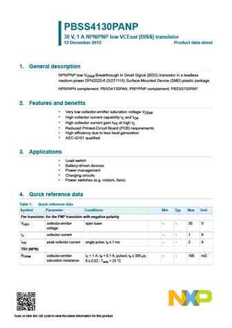
PBSS4130PANP 30 V, 1 A NPN/PNP low VCEsat (BISS) transistor 12 December 2012 Product data sheet 1. General description NPN/PNP low VCEsat Breakthrough In Small Signal (BISS) transistor in a leadless medium power DFN2020-6 (SOT1118) Surface-Mounted Device (SMD) plastic package. NPN/NPN complement PBSS4130PAN. PNP/PNP complement PBSS5130PAP. 2. Features and benefits Very low collect
pbss4130pan.pdf
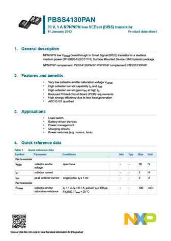
PBSS4130PAN 30 V, 1 A NPN/NPN low VCEsat (BISS) transistor 11 January 2013 Product data sheet 1. General description NPN/NPN low VCEsat Breakthrough In Small Signal (BISS) transistor in a leadless medium power DFN2020-6 (SOT1118) Surface-Mounted Device (SMD) plastic package. NPN/PNP complement PBSS4130PANP. PNP/PNP complement PBSS5130PAP. 2. Features and benefits Very low collecto
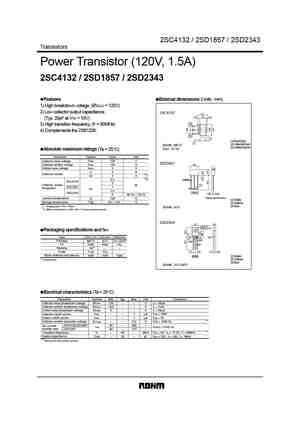
2sc4132 2sd1857.pdf
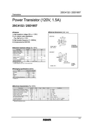
2SC4132 / 2SD1857 Transistors Power Transistor (120V, 1.5A) 2SC4132 / 2SD1857 External dimensions (Unit mm) Features 1) High breakdown voltage. (BVCEO = 120V) 2) Low collector output capacitance. 2SC4132 4.0 1.0 2.5 0.5 (Typ. 20pF at VCB = 10V) (1) 3) High transition frequency. (fT = 80MHz) (2) 4) Complements the 2SB1236. (3) (1) Base(Gate) (2) Collector(Drain) RO
2sc5659 2sc5659 2sc4618 2sc4098 2sc2413k.pdf
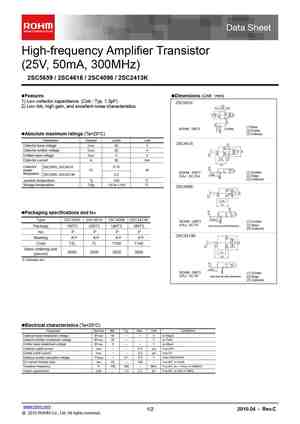
High-frequency Amplifier Transistor (25V, 50mA, 300MHz) 2SC5659 / 2SC4618 / 2SC4098 / 2SC2413K Features Dimensions (Unit mm) 1) Low collector capacitance. (Cob Typ. 1.3pF) 2SC5659 1.2 2) Low rbb, high gain, and excellent noise characteristics. 0.2 0.8 0.2 (2) (3) (1) (1) Base 0.15Max. ROHM VMT3 (2) Emitter Absolute maximum ratings (Ta=25 C) (3) Collector
2sc4132.pdf
2SC4132 / 2SD1857 / 2SD2343 Transistors Power Transistor (120V, 1.5A) 2SC4132 / 2SD1857 / 2SD2343 Features External dimensions (Units mm) 1) High breakdown voltage. (BVCEO = 120V) 2) Low collector output capacitance. 2SC4132 4.0 1.0 2.5 0.5 (Typ. 20pF at VCB = 10V) (1) 3) High transition frequency. (fT = 80MHz) (2) 4) Complements the 2SB1236. (3) (1) Base(Gate) (2) Collecto
2sc4137.pdf
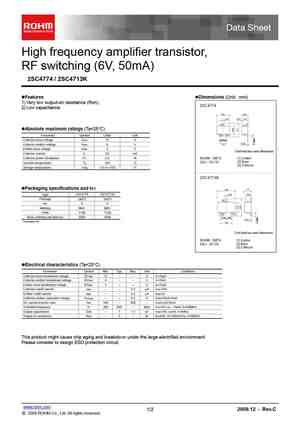
High frequency amplifier transistor, RF switching (6V, 50mA) 2SC4774 / 2SC4713K Features Dimensions (Unit mm) 1) Very low output-on resistance (Ron). 2SC4774 2) Low capacitance. 2.0 0.9 0.3 0.2 0.7 (3) Absolute maximum ratings (Ta=25 C) Parameter Symbol Limits Unit (2) (1) Collector-base voltage VCBO 12 V 0.65 0.65 0.15 Collector-emitter voltage VCEO 6 V 1.3
si4413ady.pdf
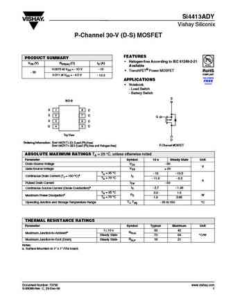
Si4413ADY Vishay Siliconix P-Channel 30-V (D-S) MOSFET FEATURES PRODUCT SUMMARY Halogen-free According to IEC 61249-2-21 VDS (V) RDS(on) ( )ID (A) Available 0.0075 at VGS = - 10 V - 15 TrenchFET Power MOSFET - 30 0.011 at VGS = - 4.5 V - 12.3 APPLICATIONS Notebook - Load Switch - Battery Switch S SO-8 S 1 8 D S 2 7 D G S 3 6 D G 4 5 D Top View
sia413dj.pdf
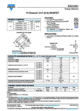
SiA413DJ Vishay Siliconix P-Channel 12-V (D-S) MOSFET FEATURES PRODUCT SUMMARY TrenchFET Power MOSFET VDS (V) RDS(on) ( )ID (A) Qg (Typ.) New Thermally Enhanced PowerPAK SC-70 Package 0.029 at VGS = - 4.5 V - 12a - Small Footprint Area 0.034 at VGS = - 2.5 V - 12a - Low On-Resistance - 12 23 nC 0.044 at VGS = - 1.8 V - 12a Material categorization 0.1
sis413dn.pdf
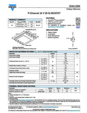
SiS413DN Vishay Siliconix P-Channel 30 V (D-S) MOSFET FEATURES PRODUCT SUMMARY TrenchFET Power MOSFET VDS (V) RDS(on) ( ) Max. ID (A) Qg (Typ.) 100% Rg and UIS Tested Material categorization 0.0094 at VGS = - 10 V - 18d - 30 35.4 nC For definitions of compliance please see 0.0132 at VGS = - 4.5 V - 18d www.vishay.com/doc?99912 PowerPAK 1212-8 APPLICATIONS
si1413dh.pdf
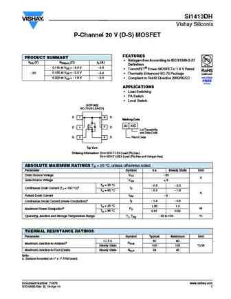
Si1413DH Vishay Siliconix P-Channel 20 V (D-S) MOSFET FEATURES PRODUCT SUMMARY Halogen-free According to IEC 61249-2-21 VDS (V) RDS(on) ( )ID (A) Definition 0.115 at VGS = - 4.5 V - 2.9 TrenchFET Power MOSFETs 1.8 V Rated 0.155 at VGS = - 2.5 V - 20 - 2.4 Thermally Enhanced SC-70 Package 0.220 at VGS = - 1.8 V - 2.0 Compliant to RoHS Directive 2002/9
si4413ad.pdf
Si4413ADY Vishay Siliconix P-Channel 30-V (D-S) MOSFET FEATURES PRODUCT SUMMARY Halogen-free According to IEC 61249-2-21 VDS (V) RDS(on) ( )ID (A) Available 0.0075 at VGS = - 10 V - 15 TrenchFET Power MOSFET - 30 0.011 at VGS = - 4.5 V - 12.3 APPLICATIONS Notebook - Load Switch - Battery Switch S SO-8 S 1 8 D S 2 7 D G S 3 6 D G 4 5 D Top View
si1413edh.pdf
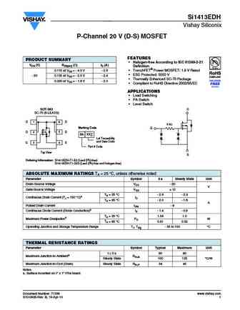
Si1413EDH Vishay Siliconix P-Channel 20 V (D-S) MOSFET FEATURES PRODUCT SUMMARY Halogen-free According to IEC 61249-2-21 VDS (V) RDS(on) ( )ID (A) Definition 0.115 at VGS = - 4.5 V - 2.9 TrenchFET Power MOSFET 1.8 V Rated ESD Protected 3000 V - 20 0.155 at VGS = - 2.5 V - 2.4 Thermally Enhanced SC-70 Package 0.220 at VGS = - 1.8 V - 2.0 Compliant to
si4413dy.pdf
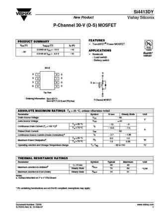
Si4413DY New Product Vishay Siliconix P-Channel 30-V (D-S) MOSFET FEATURES PRODUCT SUMMARY TrenchFET Power MOSFET VDS (V) rDS(on) ( )ID (A) Pb-free 0.0095 at VGS = - 10 V - 13 Available APPLICATIONS - 30 RoHS* 0.0145 at VGS = - 4.5 V - 10 Notebook COMPLIANT - Load switch - Battery switch SO-8 S S 1 8 D S D 2 7 S 3 6 D G G D 4 5 Top View D Ordering
sib413dk.pdf
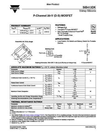
New Product SiB413DK Vishay Siliconix P-Channel 20-V (D-S) MOSFET FEATURES PRODUCT SUMMARY Halogen-free VDS (V) RDS(on) ( ) ID (A)a, f Qg (Typ.) TrenchFET Power MOSFET 0.075 at VGS = - 4.5 V - 9 New Thermally Enhanced PowerPAK RoHS - 20 4.56 nC 0.143 at VGS = - 2.5 V - 7.8 COMPLIANT SC-75 Package - Small Footprint Area APPLICATIONS Load Switch, PA Switc
sia413adj.pdf
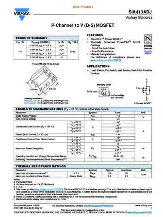
New Product SiA413ADJ Vishay Siliconix P-Channel 12 V (D-S) MOSFET FEATURES PRODUCT SUMMARY TrenchFET Power MOSFET VDS (V) RDS(on) ( ) (Max.) ID (A) Qg (Typ.) Thermally Enhanced PowerPAK SC-70 Package 0.029 at VGS = - 4.5 V - 12a - Small Footprint Area 0.034 at VGS = - 2.5 V - 12a - Low On-Resistance - 12 23 nC 0.044 at VGS = - 1.8 V - 12a Material cat
si4136dy.pdf
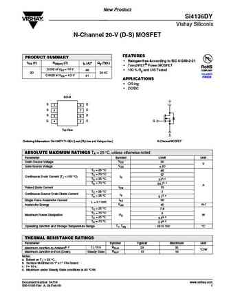
New Product Si4136DY Vishay Siliconix N-Channel 20-V (D-S) MOSFET FEATURES PRODUCT SUMMARY Halogen-free According to IEC 61249-2-21 VDS (V) RDS(on) ( ) ID (A)a Qg (Typ.) TrenchFET Power MOSFET 0.002 at VGS = 10 V 46 100 % Rg and UIS Tested 20 34 nC 0.0025 at VGS = 4.5 V 41 APPLICATIONS OR-ing DC/DC SO-8 D SD 1 8 SD 2 7 SD 3 6 GD G 4 5
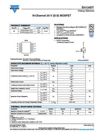
si4134dy.pdf
Si4134DY Vishay Siliconix N-Channel 30 V (D-S) MOSFET FEATURES PRODUCT SUMMARY Halogen-free According to IEC 61249-2-21 VDS (V) RDS(on) ( )ID (A)a Qg (Typ.) Definition 0.014 at VGS = 10 V 14 TrenchFET Power MOSFET 30 7.3 nC 0.0175 at VGS = 4.5 V 12.5 100 % Rg and UIS Tested Compliant to RoHS Directive 2002/95/EC APPLICATIONS SO-8 DC/DC Conversion -
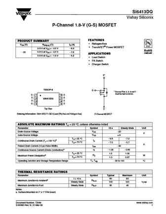
si6413dq.pdf
Si6413DQ Vishay Siliconix P-Channel 1.8-V (G-S) MOSFET FEATURES PRODUCT SUMMARY Halogen-free VDS (V) RDS(on) ( )ID (A) TrenchFET Power MOSFET 0.010 at VGS = - 4.5 V - 8.8 RoHS 0.013 at VGS = - 2.5 V - 20 - 7.6 COMPLIANT APPLICATIONS 0.016 at VGS = - 1.8 V - 6.8 Load Switch PA Switch Charger Switch S* TSSOP-8 G * Source Pins 2, 3, 6 and 7
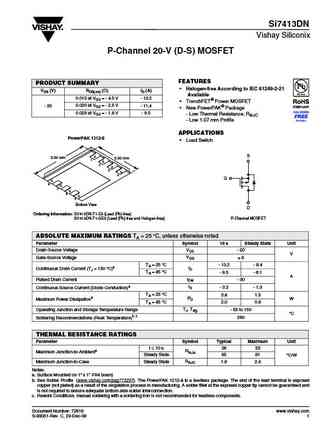
si7413dn.pdf
Si7413DN Vishay Siliconix P-Channel 20-V (D-S) MOSFET FEATURES PRODUCT SUMMARY Halogen-free According to IEC 61249-2-21 VDS (V) RDS(on) ( )ID (A) Available 0.015 at VGS = - 4.5 V - 13.2 TrenchFET Power MOSFET 0.020 at VGS = - 2.5 V - 20 - 11.4 New PowerPAK Package 0.029 at VGS = - 1.8 V - 9.5 - Low Thermal Resistance, RthJC - Low 1.07 mm Profile APPLI
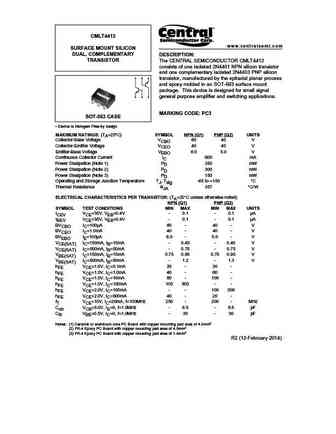
cmlt4413.pdf
CMLT4413 www.centralsemi.com SURFACE MOUNT SILICON DUAL, COMPLEMENTARY DESCRIPTION TRANSISTOR The CENTRAL SEMICONDUCTOR CMLT4413 consists of one isolated 2N4401 NPN silicon transistor and one complementary isolated 2N4403 PNP silicon transistor, manufactured by the epitaxial planar process and epoxy molded in an SOT-563 surface mount package. This device is designed for small s
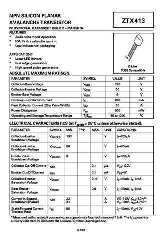
ztx413.pdf
NPN SILICON PLANAR ZTX413 AVALANCHE TRANSISTOR PROVISIONAL DATASHEET ISSUE 2 MARCH 94 T I i I i i I TI D i V i E-Line i I TO92 Compatible ABSOLUTE MAXIMUM RATINGS. T V IT II V I V V II i V I V V i V I V V i II I II I i I Di i i i T T T ELECTRICAL CHARACTERISTICS (at Tamb = 25 C unless otherwise stated). 80 T I T IT DITI II i V V I
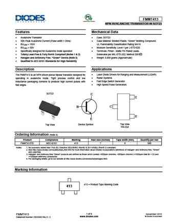
fmmt413.pdf
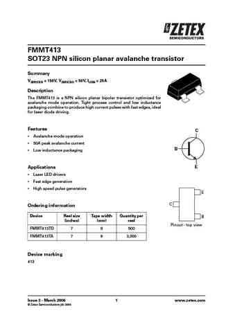
FMMT413 NPN AVALANCHE TRANSISTOR IN SOT23 Features Mechanical Data Avalanche Transistor Case SOT23 50A Peak Avalanche Current (Pulse width = 20ns) Case Material Molded Plastic. Green Molding Compound. BVCES > 150V UL Flammability Classification Rating 94V-0 BVCEO > 50V Moisture Sensitivity Level 1 per J-STD-020 Specifically designed for Av
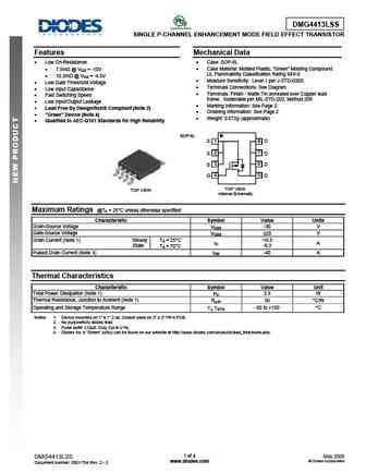
dmg4413lss.pdf
DMG4413LSS SINGLE P-CHANNEL ENHANCEMENT MODE FIELD EFFECT TRANSISTOR Features Mechanical Data Low On-Resistance Case SOP-8L 7.5m @ VGS = -10V Case Material Molded Plastic, Green Molding Compound. UL Flammability Classification Rating 94V-0 10.2m @ VGS = -4.5V Moisture Sensitivity Level 1 per J-STD-020D Low Gate Threshold Voltage Ter
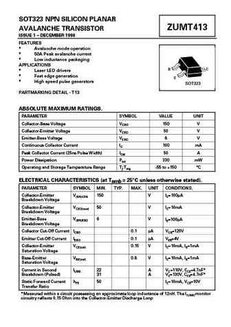
zumt413.pdf
SOT323 NPN SILICON PLANAR ZUMT413 AVALANCHE TRANSISTOR ISSUE 1 DECEMBER 1998 FEATURES * Avalanche mode operation * 50A Peak avalanche current * Low inductance packaging APPLICATIONS * Laser LED drivers * Fast edge generation * High speed pulse generators PARTMARKING DETAIL - T13 ABSOLUTE MAXIMUM RATINGS. PARAMETER SYMBOL VALUE UNIT Collector-Base Voltage VCBO 150 V Collector
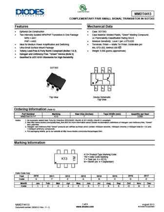
mmdt4413.pdf
MMDT4413 COMPLEMENTARY PAIR SMALL SIGNAL TRANSISTOR IN SOT363 Features Mechanical Data Epitaxial Die Construction Case SOT363 Two Internally Isolated NPN/PNP Transistors in One Package Case Material Molded Plastic, Green Molding Compound. NPN = 4401 UL Flammability Classification Rating 94V-0 PNP = 4403 Moisture Sensitivity Level 1 per J-STD-020 Id
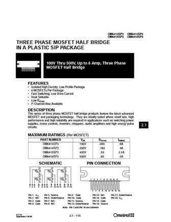
om6413sp3.pdf
OM6413SP3 OM6415SP3 OM6414SP3 OM6416SP3 THREE PHASE MOSFET HALF BRIDGE IN A PLASTIC SIP PACKAGE 100V Thru 500V, Up to 6 Amp, Three Phase MOSFET Half Bridge FEATURES Isolated High Density, Low Profile Package 6 MOSFETs Per Package Fast Switching, Low Drive Current Heat Sinkable Low RDS(on) P-Channel Also Available DESCRIPTION This series of three phase MOSF
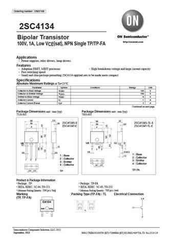
2sc4134.pdf
Ordering number EN2510B 2SC4134 Bipolar Transistor http //onsemi.com ( ) 100V, 1A, Low VCE sat , NPN Single TP/TP-FA Applications Power supplies, relay drivers, lamp drivers Features Adoption FBET, MBIT processes High breakdown voltage and large current capacity Fast switching speed Small and slim package permitting 2SC4134-applied sets to be made more compact
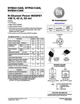
ntb6413ang ntp6413ang.pdf
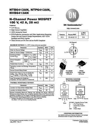
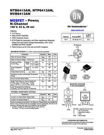
NTB6413AN, NTP6413AN, NVB6413AN N-Channel Power MOSFET 100 V, 42 A, 28 mW Features Low RDS(on) http //onsemi.com High Current Capability 100% Avalanche Tested ID MAX NVB Prefix for Automotive and Other Applications Requiring V(BR)DSS RDS(ON) MAX (Note 1) Unique Site and Control Change Requirements; AEC-Q101 100 V 28 mW @ 10 V 42 A Qualified and PPAP Capable The
ntd5413n ntd5413nt4g.pdf
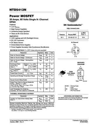
NTD5413N Power MOSFET 30 Amps, 60 Volts Single N-Channel DPAK Features Low RDS(on) http //onsemi.com High Current Capability Avalanche Energy Specified ID MAX These are Pb-Free Devices V(BR)DSS RDS(ON) MAX (Note 1) Applications 60 V 26 mW @ 10 V 30 A LED Lighting and LED Backlight Drivers DC-DC Converters N-Channel DC Motor Drivers D Switch Mod
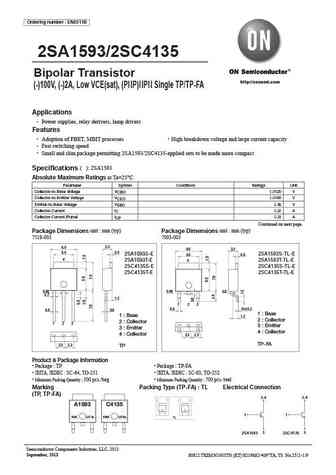
2sa1593s-e 2sa1593s 2sa1593t-e 2sa1593t 2sc4135s-e 2sc4135s 2sc4135t-e 2sc4135t.pdf
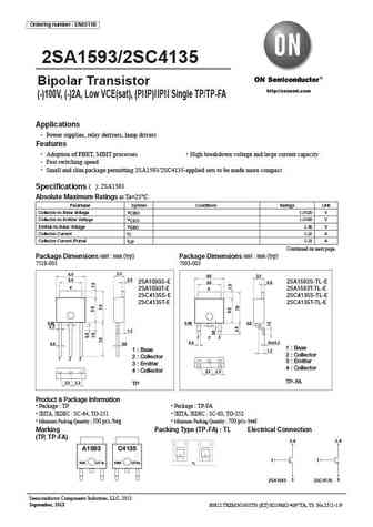
Ordering number EN2511B 2SA1593/2SC4135 Bipolar Transistor http //onsemi.com (-)100V, (-)2A, Low VCE(sat), (PNP)NPN Single TP/TP-FA Applications Power supplies, relay derivers, lamp drivers Features Adoption of FBET, MBIT processes High breakdown voltage and large current capacity Fast switching speed Small and slim package permitting 2SA1593/2SC4135-applied se
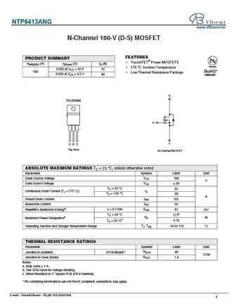
ntb6413an ntp6413an nvb6413an.pdf
NTB6413AN, NTP6413AN, NVB6413AN MOSFET Power, N-Channel 100 V, 42 A, 28 mW www.onsemi.com Features Low RDS(on) ID MAX High Current Capability V(BR)DSS RDS(ON) MAX (Note 1) 100% Avalanche Tested 100 V 28 mW @ 10 V 42 A NVB Prefix for Automotive and Other Applications Requiring Unique Site and Control Change Requirements; AEC-Q101 Qualified and PPAP Capable N-C
2sc4134s-e 2sc4134s 2sc4134t-e 2sc4134t.pdf
Ordering number EN2510B 2SC4134 Bipolar Transistor http //onsemi.com ( ) 100V, 1A, Low VCE sat , NPN Single TP/TP-FA Applications Power supplies, relay drivers, lamp drivers Features Adoption FBET, MBIT processes High breakdown voltage and large current capacity Fast switching speed Small and slim package permitting 2SC4134-applied sets to be made more compact
2sa1593 2sc4135.pdf
Ordering number EN2511B 2SA1593/2SC4135 Bipolar Transistor http //onsemi.com (-)100V, (-)2A, Low VCE(sat), (PNP)NPN Single TP/TP-FA Applications Power supplies, relay derivers, lamp drivers Features Adoption of FBET, MBIT processes High breakdown voltage and large current capacity Fast switching speed Small and slim package permitting 2SA1593/2SC4135-applied se
nvb6413an.pdf
NTB6413AN, NTP6413AN, NVB6413AN N-Channel Power MOSFET 100 V, 42 A, 28 mW Features Low RDS(on) www.onsemi.com High Current Capability 100% Avalanche Tested ID MAX NVB Prefix for Automotive and Other Applications Requiring V(BR)DSS RDS(ON) MAX (Note 1) Unique Site and Control Change Requirements; AEC-Q101 100 V 28 mW @ 10 V 42 A Qualified and PPAP Capable These
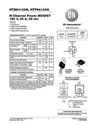
ntb6413an ntp6413an.pdf
NTB6413AN, NTP6413AN N-Channel Power MOSFET 100 V, 42 A, 28 mW Features Low RDS(on) High Current Capability http //onsemi.com 100% Avalanche Tested These are Pb-Free Devices ID MAX V(BR)DSS RDS(ON) MAX (Note 1) MAXIMUM RATINGS (TJ = 25 C Unless otherwise specified) 100 V 28 mW @ 10 V 42 A Parameter Symbol Value Unit Drain-to-Source Voltage VDSS 100 V N-Channel G
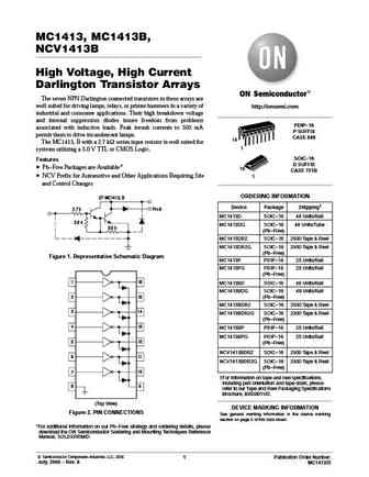
mc1413bd.pdf
MC1413, MC1413B, NCV1413B High Voltage, High Current Darlington Transistor Arrays The seven NPN Darlington connected transistors in these arrays are well suited for driving lamps, relays, or printer hammers in a variety of http //onsemi.com industrial and consumer applications. Their high breakdown voltage and internal suppression diodes insure freedom from problems PDIP-16 associated
mc1413.pdf
MC1413, MC1413B, NCV1413B High Voltage, High Current Darlington Transistor Arrays The seven NPN Darlington connected transistors in these arrays are well suited for driving lamps, relays, or printer hammers in a variety of http //onsemi.com industrial and consumer applications. Their high breakdown voltage and internal suppression diodes insure freedom from problems PDIP-16 associated
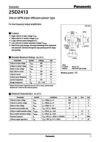
2sd2413 e.pdf
Transistor 2SD2413 Silicon NPN triple diffusion planer type For low-frequency output amplification Unit mm 1.5 0.1 4.5 0.1 1.6 0.2 Features High collector to base voltage VCBO. High collector to emitter voltage VCEO. 45 Large collector power dissipation PC. Low collector to emitter saturation voltage VCE(sat). 0.4 0.08 Mini Power type package, allowing downsizing of th
2sd2413.pdf
Transistor 2SD2413 Silicon NPN triple diffusion planer type For low-frequency output amplification Unit mm 1.5 0.1 4.5 0.1 1.6 0.2 Features High collector to base voltage VCBO. High collector to emitter voltage VCEO. 45 Large collector power dissipation PC. Low collector to emitter saturation voltage VCE(sat). 0.4 0.08 Mini Power type package, allowing downsizing of th
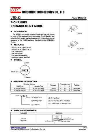
utd413.pdf
UNISONIC TECHNOLOGIES CO., LTD UTD413 Power MOSFET P-CHANNEL ENHANCEMENT MODE DESCRIPTION The UTD413 can provide excellent RDS(ON) and low gate charge by using UTC s advanced trench technology. The UTD413 is well suited for high current load applications with the excellent thermal resistance of the TO-252 package. Standard Product UTD413 is Pb-free. FEATURES * RD
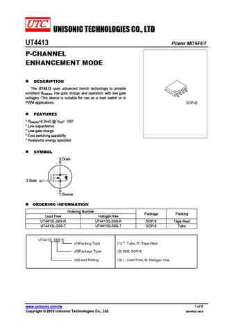
ut4413.pdf
UNISONIC TECHNOLOGIES CO., LTD UT4413 Power MOSFET P-CHANNEL ENHANCEMENT MODE DESCRIPTION The UT4413 uses advanced trench technology to provide excellent RDS(ON), low gate charge and operation with low gate voltages. This device is suitable for use as a load switch or in PWM applications. FEATURES * RDS(ON)=8.5m @ VGS= -10V * Low capacitance * Low gate charge *
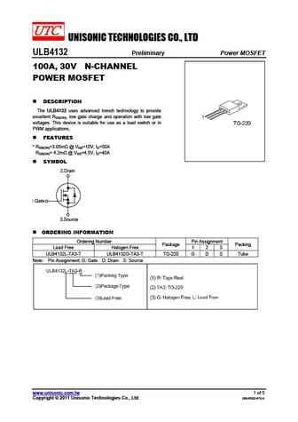
ulb4132.pdf
UNISONIC TECHNOLOGIES CO., LTD ULB4132 Preliminary Power MOSFET 100A, 30V N-CHANNEL POWER MOSFET DESCRIPTION The ULB4132 uses advanced trench technology to provide excellent RDS(ON), low gate charge and operation with low gate voltages. This device is suitable for use as a load switch or in PWM applications. FEATURES * RDS(ON)=3.05m @ VGS=10V, ID=50A * RDS(ON)= 4.2m
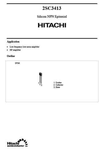
2sc3413.pdf
2SC3413 Silicon NPN Epitaxial Application Low frequency low noise amplifier HF amplifier Outline SPAK 1. Emitter 1 2 2. Collector 3 3. Base 2SC3413 Absolute Maximum Ratings (Ta = 25 C) Item Symbol Ratings Unit Collector to base voltage VCBO 40 V Collector to emitter voltage VCEO 30 V Emitter to base voltage VEBO 5V Collector current IC 100 mA Collector power dissip
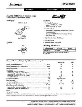
huf76413p3.pdf
HUF76413P3 Data Sheet November 1999 File Number 4723.1 22A, 60V, 0.056 Ohm, N-Channel, Logic Level UltraFET Power MOSFET Packaging Features JEDEC TO-220AB Ultra Low On-Resistance - rDS(ON) = 0.049 , VGS = 10V SOURCE - rDS(ON) = 0.056 , VGS = 5V DRAIN GATE Simulation Models - Temperature Compensated PSPICE and SABER Electrical Models - Spice and SABER Thermal Im
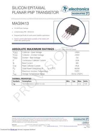
mag9413.pdf
Downloaded from Elcodis.com electronic components distributor Downloaded from Elcodis.com electronic components distributor Downloaded from Elcodis.com electronic components distributor Downloaded from Elcodis.com electronic components distributor
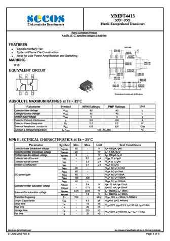
mmdt4413.pdf
MMDT4413 NPN - PNP Plastic-Encapsulated Transistors Elektronische Bauelemente RoHS Compliant Product A suffix of -C specifies halogen & lead-free FEATURES SOT-363 Complementary Pair o .055(1.40) 8 .047(1.20) .026TYP 0o Epitaxial Planar Die Construction (0.65TYP) Ideal for Low Power Amplification and Switching .021REF (0.525)REF MARKING .053(1.35) .096(2.
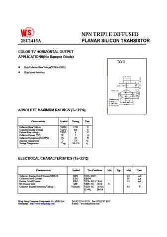
2sc1413a.pdf
NPN TRIPLE DIFFUSED 2SC1413A PLANAR SILICON TRANSISTOR COLOR TV HORIZONTAL OUTPUT APPLICATIONS(No Damper Diode) TO-3 High Collector-Base Voltage(VCBO=1500V) High Speed Switching ABSOLUTE MAXIMUM RATINGS (Ta=25 C C) C C Characteristic Symbol Rating Unit Collector-Base Voltage VCBO 1500 V Collector-Emitter Voltage VCEO 800 V Emitter-Base voltage VEBO 6 V Collector Current
gc520-k gc521-k gc522-k bc413b-c kc147 kc148 kc149 kc237a-b-v kc238a-b-c kc239f-b-c kc507 kc508 kc509 kc635 kc637 kc639.pdf
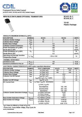
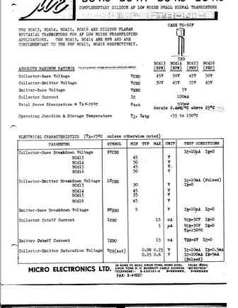
bc413 bc414 b c.pdf
Continental Device India Limited An ISO/TS 16949, ISO 9001 and ISO 14001 Certified Company BC413, B, C NPN SILICON PLANAR EPITAXIAL TRANSISTORS BC414, B, C TO-92 Plastic Package E B C ABSOLUTE MAXIMUM RATINGS (Ta=25 C) DESCRIPTION SYMBOL BC413 BC414 UNITS Collector Emitter Voltage VCEO 30 45 V Collector Base Voltage VCBO 45 50 V Emitter Base Voltage VEBO 5.0 V Collector Current
mmdt4413.pdf
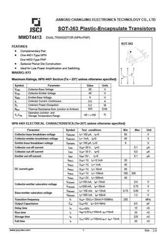
JIANGSU CHANGJING ELECTRONICS TECHNOLOGY CO., LTD SOT-363 Plastic-Encapsulate Transistors DUAL TRANSISTOR (NPN+PNP) MMDT4413 SOT-363 FEATURES Complementary Pair One 4401-Type NPN One 4403-Type PNP Epitaxial Planar Die Construction Ideal for Low Power Amplification and Switching MAKING K13 Maximum Ratings, NPN 4401 Section (Ta = 25 unless otherwise specified) Symbol Pa
ktd1413.pdf
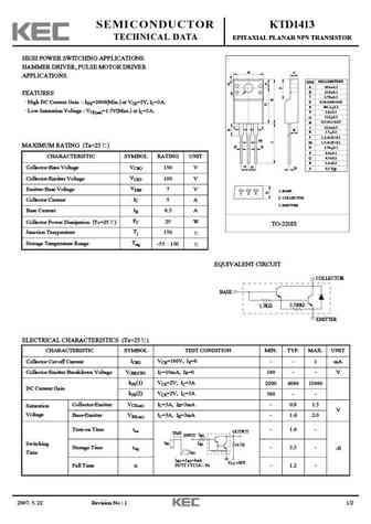
SEMICONDUCTOR KTD1413 TECHNICAL DATA EPITAXIAL PLANAR NPN TRANSISTOR HIGH POWER SWITCHING APPLICATIONS. HAMMER DRIVER, PULSE MOTOR DRIVER A C APPLICATIONS. DIM MILLIMETERS S _ A 10.0 0.3 + _ + B 15.0 0.3 E FEATURES C _ 2.70 0.3 + D 0.76+0.09/-0.05 High DC Current Gain hFE=2000(Min.) at VCE=2V, IC=3A. _ E 3.2 0.2 + Low Saturation Voltage VCE(sat)=1.5V(Max.) at IC
krc413.pdf
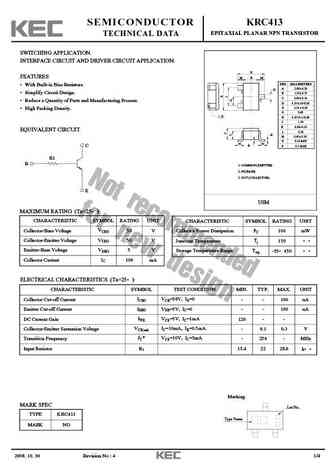
SEMICONDUCTOR KRC413 EPITAXIAL PLANAR NPN TRANSISTOR TECHNICAL DATA SWITCHING APPLICATION. INTERFACE CIRCUIT AND DRIVER CIRCUIT APPLICATION. E FEATURES M B M DIM MILLIMETERS With Built-in Bias Resistors. _ + A 2.00 0.20 D 2 _ Simplify Circuit Design. B 1.25 0.15 + _ + C 0.90 0.10 3 Reduce a Quantity of Parts and Manufacturing Process. 1 D 0.3+0.10/-0.05 _ + E 2
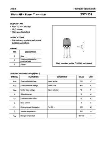
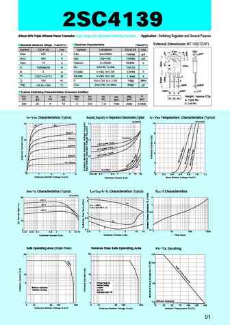
2sc4139.pdf
2SC4139 Silicon NPN Triple Diffused Planar Transistor (High Voltage and High Speed Switchihg Transistor) Application Switching Regulator and General Purpose External Dimensions MT-100(TO3P) Absolute maximum ratings (Ta=25 C) Electrical Characteristics (Ta=25 C) Symbol 2SC4139 Symbol Conditions 2SC4139 Unit Unit 0.2 4.8 0.4 15.6 0.1 9.6 2.0 VCBO 500 ICBO VCB=500V 100max
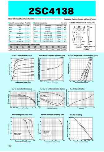
2sc4138.pdf
2SC4138 Silicon NPN Triple Diffused Planar Transistor (High Voltage and High Speed Switchihg Transistor) Application Switching Regulator and General Purpose External Dimensions MT-100(TO3P) Absolute maximum ratings (Ta=25 C) Electrical Characteristics (Ta=25 C) Symbol 2SC4138 Unit Symbol Conditions 2SC4138 Unit 0.2 4.8 0.4 15.6 ICBO 0.1 VCBO 500 V VCB=500V 100max A 2.0
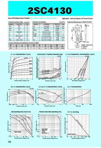
2sc4130.pdf
2SC4130 Silicon NPN Epitaxial Planar Transistor (High Voltage and High Speed Switchihg Transistor) Application Switching Regulator and General Purpose Absolute maximum ratings (Ta=25 C) Electrical Characteristics (Ta=25 C) External Dimensions FM20(TO220F) Symbol 2SC4130 Symbol Conditions 2SC4130 Unit Unit 0.2 4.2 0.2 10.1 c0.5 2.8 VCBO 500 ICBO VCB=500V 100max V A VCEO
2sc4131.pdf
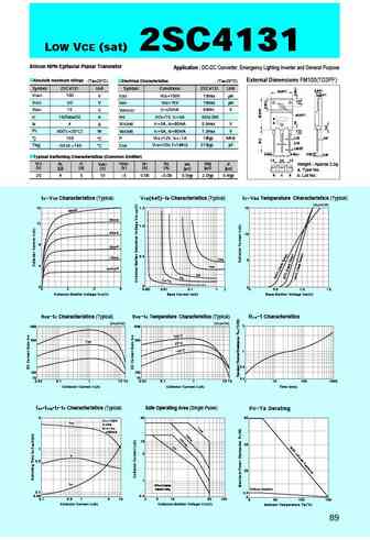
LOW VCE (sat) 2SC4131 Silicon NPN Epitaxial Planar Transistor Application DC-DC Converter, Emergency Lighting Inverter and General Purpose Absolute maximum ratings (Ta=25 C) Electrical Characteristics (Ta=25 C) External Dimensions FM100(TO3PF) Symbol 2SC4131 Unit Symbol Conditions 2SC4131 Unit 0.2 0.2 5.5 15.6 0.2 3.45 VCBO 100 VCB=100V 10max A V ICBO VCEO 50 IEBO VEB
sta413a.pdf
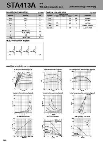
NPN With built-in avalanche diode External dimensions STA (10-pin) STA413A D Absolute maximum ratings Electrical characteristics (Ta=25 C) (Ta=25 C) Specification Symbol Ratings Unit Symbol Unit Conditions min typ max VCBO 35 5V ICBO 10 AVCB=30V VCEO 35 5V IEBO 10 AVEB=6V VEBO 6V VCEO 30 40 V IC=25mA IC 3A hFE 500 VCE=4V, IC=0.5A IB 1A VCE(sat) 0.5 V IC=1A, IB=
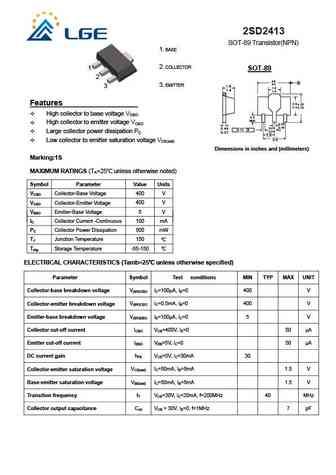
2sd2413.pdf
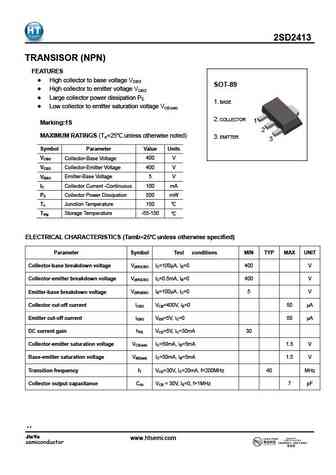
2SD2413 TRANSISOR (NPN) FEATURES High collector to base voltage VCBO SOT-89 High collector to emitter voltage VCEO Large collector power dissipation PC 1. BASE Low collector to emitter saturation voltage VCE(sat) 2. COLLECTOR 1 Marking 1S 2 MAXIMUM RATINGS (TA=25 unless otherwise noted) 3. EMITTER 3 Symbol Parameter Value Units VCBO Collector-Base Volta
mmdt4413.pdf
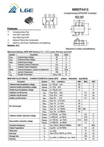
MMDT4413 Complementary NPN/PNP Transistor SOT-363 Features Complementary Pair One 4401-Type NPN, One 4403-Type PNP Epitaxial Planar Die Construction Ideal for Low Power Amplification and Switching MAKING K13 Dimensions in inches and (millimeters) Maximum Ratings, NPN 4401 Section (TA = 25 unless otherwise specified) Symbol Parameter Value Units VCBO Collector-B
2sd2413.pdf
2SD2413 SOT-89 Transistor(NPN) 1. BASE 2. COLLECTOR 1 SOT-89 2 4.6 B 4.4 3. EMITTER 1.6 3 1.8 1.4 1.4 2.6 Features 4.25 2.4 3.75 High collector to base voltage VCBO 0.8 MIN High collector to emitter voltage VCEO 0.53 0.40 0.48 0.44 2x) 0.13 B 0.35 Large collector power dissipation PC 0.37 1.5 3.0 Low collector to emitter saturation voltage VCE(
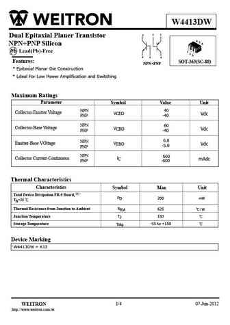
w4413dw.pdf
W4413DW 2 1 3 Dual Epitaxial Planer Transistor 6 5 4 NPN+PNP Silicon 1 2 3 4 5 6 Features SOT-363(SC-88) NPN+PNP * Epitaxial Planar Die Construction * Ldeal For Low Power Amplification and Switching Maximum Ratings Parameter Symbol Value Unit NPN 40 Collector-Emitter Voltage V CEO Vdc PNP -40 NPN 60 Collector-Base Voltage VCBO Vdc PNP -40 6.0 NPN Emitter-Base
aod4130 aoi4130.pdf
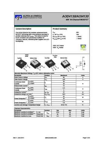
AOD4130/AOI4130 60V N-Channel MOSFET General Description Product Summary VDS 60V The AOD4130/AOI4130 combines advanced trench MOSFET technology with a low resistance package to ID (at VGS=10V) 30A provide extremely low RDS(ON). This device is ideal for RDS(ON) (at VGS=10V)
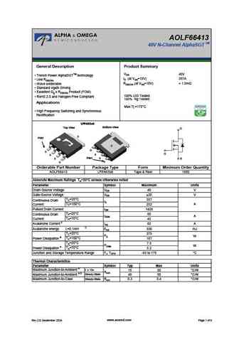
aolf66413.pdf
AOLF66413 TM 40V N-Channel AlphaSGT General Description Product Summary VDS 40V Trench Power AlphaSGTTM technology ID (at VGS=10V) 357A Low RDS(ON) RDS(ON) (at VGS=10V)
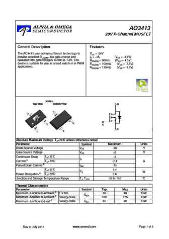
ao3413.pdf
AO3413 20V P-Channel MOSFET General Description Features General Description Features The AO3413 uses advanced trench technology to VDS = -20V The AO3413 uses advanced trench technology to VDS = -20V provide excellent RDS(ON), low gate charge and ID = -3A (VGS = -4.5V) provide excellent RDS(ON), low gate charge and ID = -3A (VGS = -4.5V) operation with gate voltages as low as 1.8V. This
ao7413.pdf
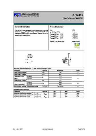
AO7413 20V P-Channel MOSFET General Description Product Summary VDS -20V The AO7413 uses advanced trench technology to provide excellent RDS(ON), low gate charge and operation with gate ID (at VGS=-10V) -1.4A voltages as low as 2.5V. This device is suitable for use as RDS(ON) (at VGS= -10V)
aod413a.pdf
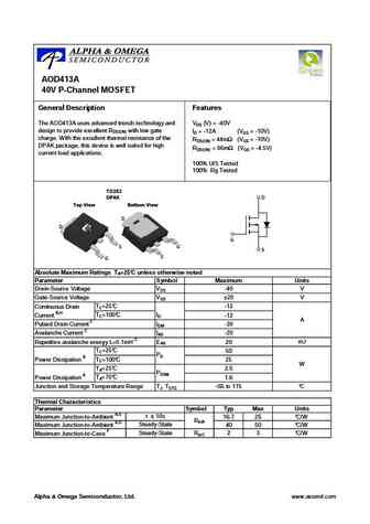
AOD413A 40V P-Channel MOSFET General Description Features The AOD413A uses advanced trench technology and VDS (V) = -40V design to provide excellent RDS(ON) with low gate ID = -12A (VGS = -10V) charge. With the excellent thermal resistance of the RDS(ON)
aoc2413.pdf
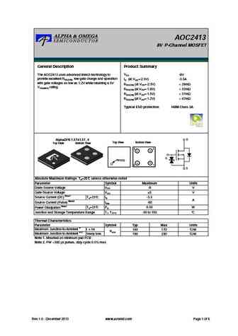
AOC2413 8V P-Channel MOSFET General Description Product Summary VDS -8V The AOC2413 uses advanced trench technology to provide excellent RDS(ON), low gate charge and operation ID (at VGS=-2.5V) -3.5A with gate voltages as low as 1.2V while retaining a 5V RDS(ON) (at VGS=-2.5V)
aod4132.pdf
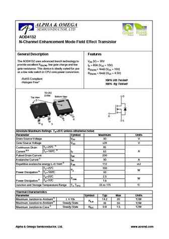
AOD4132 N-Channel Enhancement Mode Field Effect Transistor General Description Features The AOD4132 uses advanced trench technology to VDS (V) = 30V provide excellent RDS(ON), low gate charge and low ID = 85A (VGS = 10V) gate resistance. This device is ideally suited for use RDS(ON)
aod4136.pdf
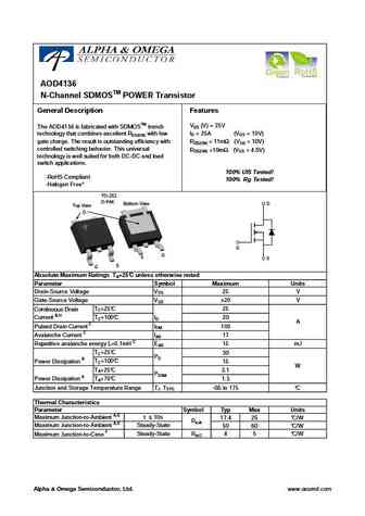
AOD4136 N-Channel SDMOSTM POWER Transistor General Description Features VDS (V) = 25V The AOD4136 is fabricated with SDMOSTM trench ID = 25A (VGS = 10V) technology that combines excellent RDS(ON) with low gate charge. The result is outstanding efficiency with RDS(ON)
aol1413.pdf
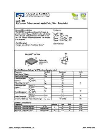
AOL1413 P-Channel Enhancement Mode Field Effect Transistor General Description Features The AOL1413 uses advanced trench technology to provide excellent RDS(ON) and ultra-low low gate charge VDS (V) = -30V with a 25V gate rating. This device is suitable for use ID = -38A (VGS = -10V) as a load switch or in PWM applications. The device is RDS(ON)
aon4413.pdf
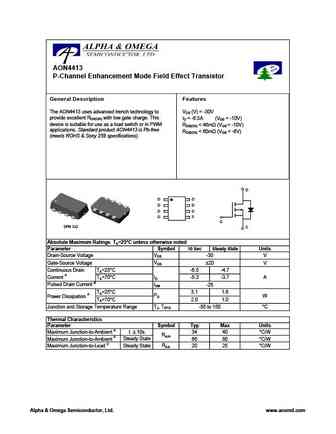
AON4413 P-Channel Enhancement Mode Field Effect Transistor General Description Features The AON4413 uses advanced trench technology to VDS (V) = -30V provide excellent RDS(ON) with low gate charge. This ID = -6.5A (VGS = -10V) device is suitable for use as a load switch or in PWM RDS(ON)
aod4130.pdf
AOD4130/AOI4130 60V N-Channel MOSFET General Description Product Summary VDS 60V The AOD4130/AOI4130 combines advanced trench MOSFET technology with a low resistance package to ID (at VGS=10V) 30A provide extremely low RDS(ON). This device is ideal for RDS(ON) (at VGS=10V)
aoi4130.pdf
AOD4130/AOI4130 60V N-Channel MOSFET General Description Product Summary VDS 60V The AOD4130/AOI4130 combines advanced trench MOSFET technology with a low resistance package to ID (at VGS=10V) 30A provide extremely low RDS(ON). This device is ideal for RDS(ON) (at VGS=10V)
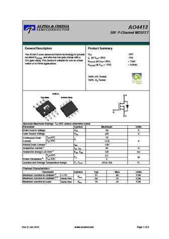
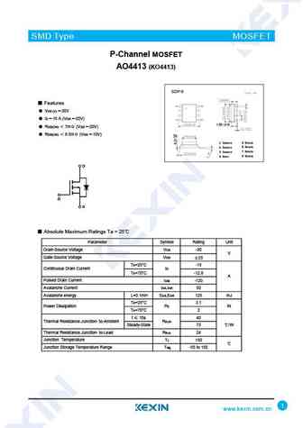
ao4413.pdf
AO4413 30V P-Channel MOSFET General Description Product Summary VDS -30V The AO4413 uses advanced trench technology to provide excellent RDS(ON), and ultra-low low gate charge with a ID (at VGS=-20V) -15A 25V gate rating. This device is suitable for use as a load RDS(ON) (at VGS=-20V)
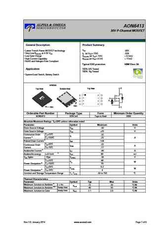
aon6413.pdf
AON6413 30V P-Channel MOSFET General Description Product Summary VDS Latest Trench Power MOSFET technology -30V Very Low RDS(ON) at 4.5V VGS ID (at VGS=-10V) -32A Low Gate Charge RDS(ON) (at VGS=-10V)
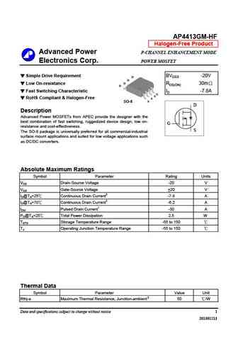
ap4413gm-hf.pdf
AP4413GM-HF Halogen-Free Product Advanced Power P-CHANNEL ENHANCEMENT MODE Electronics Corp. POWER MOSFET Simple Drive Requirement BVDSS -20V D D D Low On-resistance RDS(ON) 30m D Fast Switching Characteristic ID -7.8A G S RoHS Compliant & Halogen-Free S S SO-8 D Description Advanced Power MOSFETs from APEC provide the designer with the best combination of
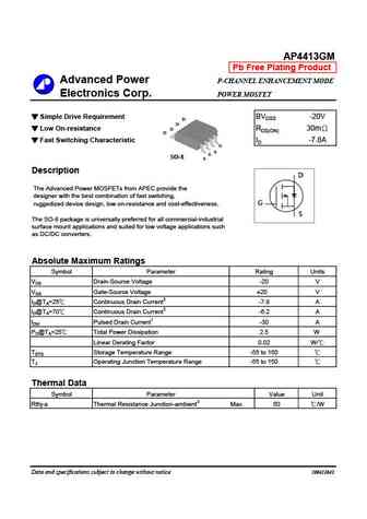
ap4413gm.pdf
AP4413GM Pb Free Plating Product Advanced Power P-CHANNEL ENHANCEMENT MODE Electronics Corp. POWER MOSFET Simple Drive Requirement BVDSS -20V D D Low On-resistance D RDS(ON) 30m D Fast Switching Characteristic ID -7.8A G S S SO-8 S Description D The Advanced Power MOSFETs from APEC provide the designer with the bes
am3413p.pdf
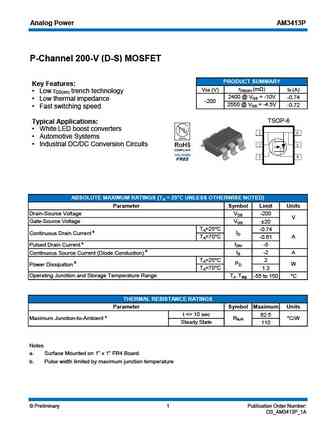
Analog Power AM3413P P-Channel 200-V (D-S) MOSFET PRODUCT SUMMARY Key Features rDS(on) (m ) VDS (V) ID (A) Low r trench technology DS(on) 2400 @ VGS = -10V -0.74 Low thermal impedance -200 2550 @ VGS = -4.5V -0.72 Fast switching speed TSOP-6 Typical Applications White LED boost converters Automotive Systems Industrial DC/DC Conversion Circuits
afp3413.pdf
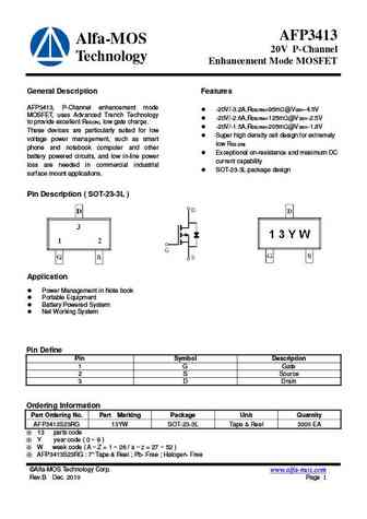
AFP3413 Alfa-MOS 20V P-Channel Technology Enhancement Mode MOSFET General Description Features AFP3413, P-Channel enhancement mode -20V/-3.2A,RDS(ON)=95m @VGS=-4.5V MOSFET, uses Advanced Trench Technology -20V/-2.6A,RDS(ON)=125m @VGS=-2.5V to provide excellent RDS(ON), low gate charge. -20V/-1.5A,RDS(ON)=205m @VGS=-1.8V These devices are particularly suited for
afp3413a.pdf
AFP3413A Alfa-MOS 20V P-Channel Technology Enhancement Mode MOSFET General Description Features AFP3413A, P-Channel enhancement mode -20V/-2.6A,RDS(ON)=120m @VGS=-4.5V MOSFET, uses Advanced Trench Technology -20V/-2.2A,RDS(ON)=170m @VGS=-2.5V to provide excellent RDS(ON), low gate charge. -20V/-1.2A,RDS(ON)=230m @VGS=-1.8V These devices are particularly suited f
afn4134.pdf
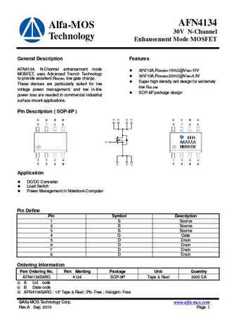
AFN4134 Alfa-MOS 30V N-Channel Technology Enhancement Mode MOSFET General Description Features AFN4134, N-Channel enhancement mode 30V/12A,RDS(ON)=15m @VGS=10V MOSFET, uses Advanced Trench Technology 30V/10A,RDS(ON)=20m @VGS=4.5V to provide excellent RDS(ON), low gate charge. Super high density cell design for extremely These devices are particularly suited for lo
afn4134w.pdf
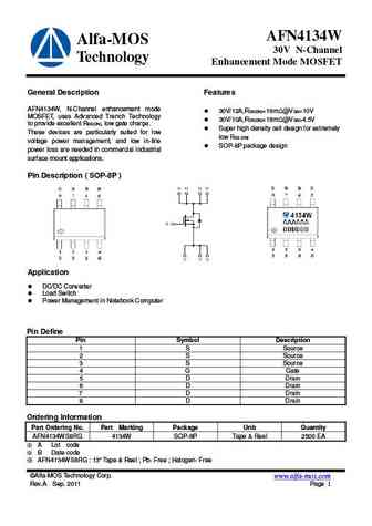
AFN4134W Alfa-MOS 30V N-Channel Technology Enhancement Mode MOSFET General Description Features AFN4134W, N-Channel enhancement mode 30V/12A,RDS(ON)=16m @VGS=10V MOSFET, uses Advanced Trench Technology 30V/10A,RDS(ON)=18m @VGS=4.5V to provide excellent RDS(ON), low gate charge. Super high density cell design for extremely These devices are particularly suited for
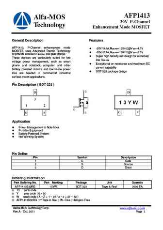
afp1413.pdf
AFP1413 Alfa-MOS 20V P-Channel Technology Enhancement Mode MOSFET General Description Features AFP1413, P-Channel enhancement mode -20V/-3.0A,RDS(ON)=125m @VGS=-4.5V MOSFET, uses Advanced Trench Technology -20V/-2.4A,RDS(ON)=160m @VGS=-2.5V to provide excellent RDS(ON), low gate charge. Super high density cell design for extremely These devices are particularly su
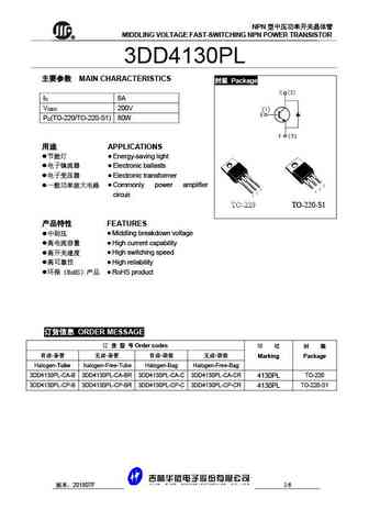
3dd4130pl.pdf
NPN MIDDLING VOLTAGE FAST-SWITCHING NPN POWER TRANSISTOR R 3DD4130PL MAIN CHARACTERISTICS Package I 8A C V 200V CEO P (TO-220/TO-220-S1) 80W C APPLICATIONS Energy-saving light Electronic ballasts Electronic transformer
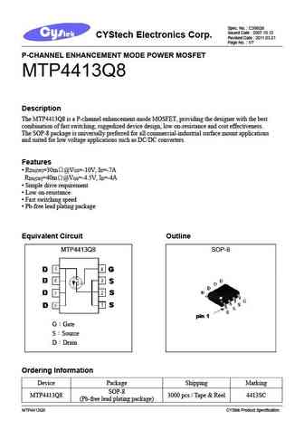
mtp4413q8.pdf
Spec. No. C398Q8 Issued Date 2007.10.12 CYStech Electronics Corp. Revised Date 2011.03.21 Page No. 1/7 P-CHANNEL ENHANCEMENT MODE POWER MOSFET MTP4413Q8 Description The MTP4413Q8 is a P-channel enhancement-mode MOSFET, providing the designer with the best combination of fast switching, ruggedized device design, low on-resistance and cost effectiveness. The SOP-8 pack
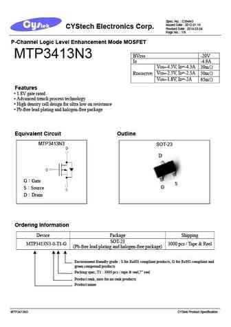
mtp3413n3.pdf
Spec. No. C394N3 Issued Date 2012.01.19 CYStech Electronics Corp. Revised Date 2014.03.04 Page No. 1/9 P-Channel Logic Level Enhancement Mode MOSFET BVDSS -20V MTP3413N3 ID -4.9A VGS=-4.5V, ID=-4.3A 39m VGS=-2.5V, ID=-2.5A RDSON(TYP) 50m VGS=-1.8V, ID=-2A 65m Features 1.8V gate rated Advanced trench process technology High density cell desig
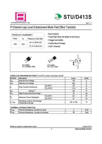
stu413s std413s.pdf
Gre r r P Pr Pr Pro STU/D413S a S mHop Microelectronics C orp. Ver 1.1 P-Channel Logic Level Enhancement Mode Field Effect Transistor FEATURES PRODUCT SUMMARY Super high dense cell design for low RDS(ON). VDSS ID RDS(ON) (m ) Max Rugged and reliable. 48 @ VGS=10V Suface Mount Package. -40V -22A 78 @ VGS=4.5V ESD Protected. G G S S STU SERIES STD SERIES ( ) TO - 252
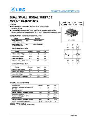
lmbt4413dw1t1g.pdf
LESHAN RADIO COMPANY, LTD. DUAL SMALL SIGNAL SURFACE MOUNT TRANSISTOR LMBT4413DW1T1G FEATURE S-LMBT4413DW1T1G We declare that the material of product is ROHS compliant 6 and halogen free. 5 4 S- Prefix for Automotive and Other Applications Requiring Unique Site and Control Change Requirements; AEC-Q101 Qualified and PPAP Capable. 1 2 DEVICE MARKING AND ORDERING INFORMATIO
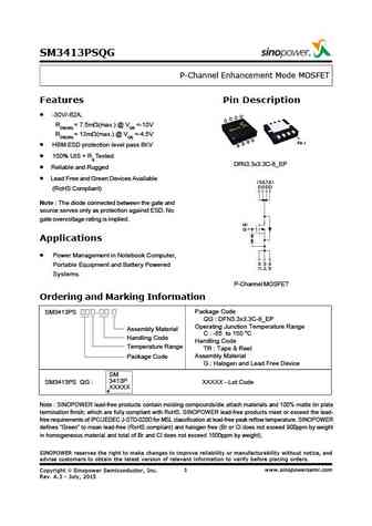
sm3413psqg.pdf
SM3413PSQG P-Channel Enhancement Mode MOSFET Features Pin Description -30V/-62A, D D D D RDS(ON) = 7.5m (max.) @ VGS =-10V RDS(ON) = 13m (max.) @ VGS =-4.5V G S Pin 1 S HBM ESD protection level pass 8KV S 100% UIS + Rg Tested DFN3.3x3.3C-8_EP Reliable and Rugged Lead Free and Green Devices Available ( 5,6,7,8 ) DDDD (RoHS Compliant) Note The diode connected
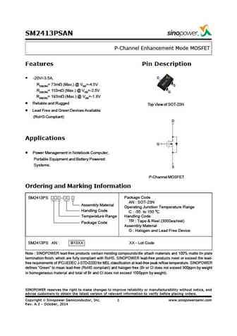
sm2413psan.pdf
SM2413PSAN P-Channel Enhancement Mode MOSFET Features Pin Description D -20V/-3.5A, RDS(ON)= 73m (Max.) @ VGS=-4.5V S RDS(ON)= 110m (Max.) @ VGS=-2.5V G RDS(ON)= 193m (Max.) @ VGS=-1.8V Reliable and Rugged Top View of SOT-23N Lead Free and Green Devices Available (RoHS Compliant) D Applications G Power Management in Notebook Computer, Portable Equipment and
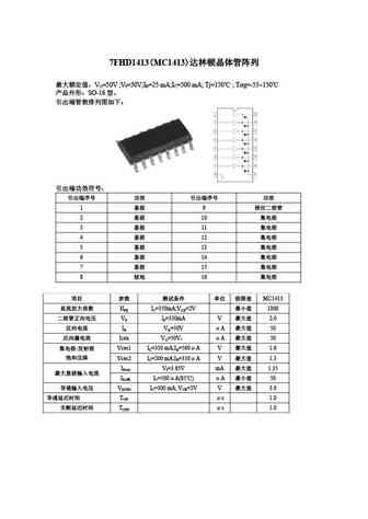
7fhd1413.pdf
7FHD1413(MC1413) VO=50V ;VI=30V;IB=25 mA;IC=500 mA; Tj=150 ; Tstg=-55 150 SO-16 1 9 2 10 3 11 4 12 5 13 6
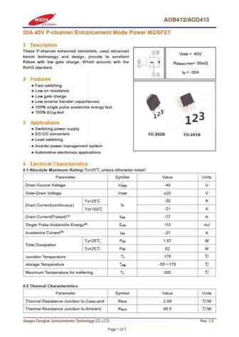
aob413 aod413.pdf
AOB413/AOD413 30A 40V P-channel Enhancement Mode Power MOSFET 1 Description These P-channel enhanced vdmosfets, used advanced V = -40V DSS trench technology and design, provide to excellent Rdson with low gate charge. Which accords with the R = 30m DS(on) (TYP) RoHS standard. I = -30A D 2 Features Fast switching Low on resistance Low gate charge Low reverse tr
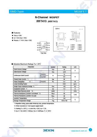
irf7413.pdf
SMD Type MOSFET N-Channel MOSFET IRF7413 (KRF7413) SOP-8 Features VDS (V) = 30V ID = 12 A (VGS = 10V) 1.50 0.15 RDS(ON) 11m (VGS = 10V) 1 8 S D 1 Source 5 Drain 2 7 S D 6 Drain 2 Source 3 6 7 Drain S D 3 Source 8 Drain 4 Gate 4 5 G D Top View Absolute Maximum Ratings Ta = 25 Parameter Symbol Rating Unit Drain-Source Voltage VDS 30 V
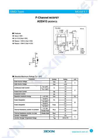
aod413.pdf
SMD Type MOSFET P-Channel MOSFET AOD413 (KOD413) TO-252 Unit mm 6.50+0.15 -0.15 +0.1 2.30 -0.1 +0.2 5.30-0.2 +0.8 0.50 -0.7 Features 4 VDS (V) =-40V ID =-12 A (VGS =-10V) RDS(ON) 45m (VGS =-10V) 0.127 0.80+0.1 max -0.1 RDS(ON) 69m (VGS =-4.5V) 1 Gate 2 Drain 2.3 0.60+ 0.1 - 0.1 3 Source +0.15 4.60 -0.15 4 Drain D G S Absol
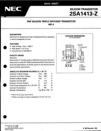
2sa1413-z.pdf
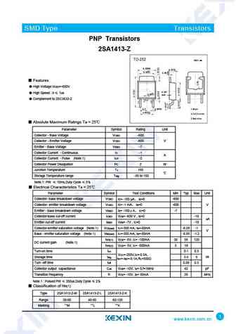
SMD Type Transistors PNP Transistors 2SA1413-Z TO-252 Unit mm +0.15 6.50-0.15 +0.1 2.30 -0.1 +0.2 5.30-0.2 +0.8 0.50 -0.7 Features High Voltage VCEO=-600V 0.127 High Speed tf 1us +0.1 0.80-0.1 max Complement to 2SC3632-Z + 0.1 1 Base 2.3 0.60- 0.1 +0.15 4.60 -0.15 2 Collector 3 Emitter Absolute Maximum Ratings Ta = 25 Parameter Symbol
ao3413-3.pdf
SMD Type MOSFET P-Channel MOSFET AO3413 (KO3413) SOT-23-3 Unit mm +0.2 2.9-0.1 +0.1 0.4 -0.1 3 Features VDS (V) =-20V ID =-3 A (VGS =-4.5V) 1 2 RDS(ON) 80m (VGS =-4.5V) +0.02 +0.1 0.15 -0.02 0.95 -0.1 RDS(ON) 100m (VGS =-2.5V) +0.1 1.9-0.2 RDS(ON) 130m (VGS =-1.8V) 1. Gate 2. Source D D 3. Drain G G S S Absolute
ao3413.pdf
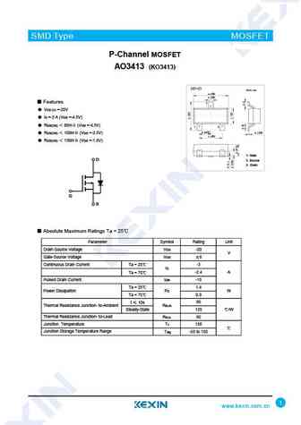
SMD Type MOSFET P-Channel MOSFET AO3413 (KO3413) SOT-23 Unit mm +0.1 2.9-0.1 +0.1 0.4 -0.1 Features 3 VDS (V) =-20V ID =-3 A (VGS =-4.5V) RDS(ON) 80m (VGS =-4.5V) 1 2 +0.1 0.95-0.1 0.1+0.05 -0.01 RDS(ON) 100m (VGS =-2.5V) +0.1 1.9-0.1 RDS(ON) 130m (VGS =-1.8V) 1. Gate D D 2. Source 3. Drain G G S S Absolute Maxim
ko3413.pdf
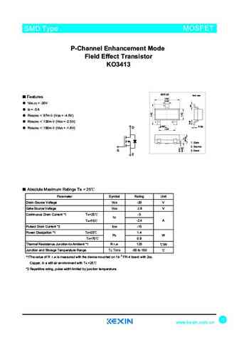
SMD Type MOSFET P-Channel Enhancement Mode Field Effect Transistor KO3413 SOT-23 Unit mm Features +0.1 2.9-0.1 +0.1 0.4-0.1 VDS (V) = -20V 3 ID = -3 A RDS(ON) 97m (VGS = -4.5V) RDS(ON) 130m (VGS = -2.5V) 1 2 +0.1 +0.05 0.95-0.1 0.1-0.01 D RDS(ON) 190m (VGS = -1.8V) +0.1 1.9-0.1 1.Base 1. Gate 2.Emitter 2. Source G 3. Dr
2sd2413.pdf
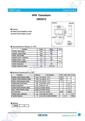
SMD Type Transistors NPN Transistors 2SD2413 SOT-89 Unit mm 1.70 0.1 Features Collector Current Capability IC=100mA Collector Emitter Voltage VCEO=400V 0.42 0.1 0.46 0.1 1.Base 2.Collector 3.Emitter Absolute Maximum Ratings Ta = 25 Parameter Symbol Rating Unit Collector - Base Voltage VCBO 400 Collector - Emitter Voltage VCEO 400 V Emitter - Base Voltag
ao4413.pdf
SMD Type MOSFET P-Channel MOSFET AO4413 (KO4413) SOP-8 Features VDS (V) =-30V ID =-15 A (VGS =-20V) 1.50 0.15 RDS(ON) 7m (VGS =-20V) RDS(ON) 8.5m (VGS =-10V) 1 Source 5 Drain 6 Drain 2 Source 7 Drain 3 Source 8 Drain 4 Gate D D G G S S Absolute Maximum Ratings Ta = 25 Parameter Symbol Rating Unit Drain-Source Voltage VDS -30
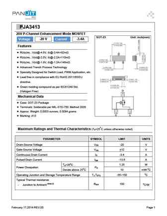
pja3413.pdf
PPJA3413 20V P-Channel Enhancement Mode MOSFET SOT-23 Unit inch(mm) Voltage -20 V Current -3.4A Features RDS(ON) , VGS@-4.5V, ID@-3.4A
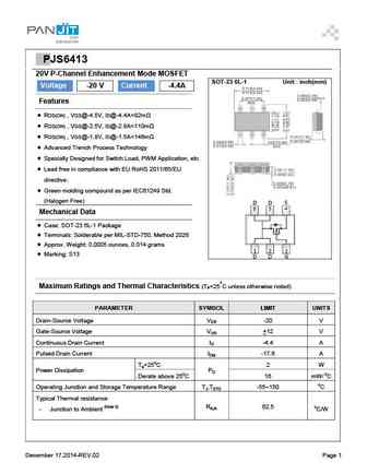
pjs6413.pdf
PPJS6413 20V P-Channel Enhancement Mode MOSFET SOT-23 6L-1 Unit inch(mm) Voltage -20 V Current -4.4A Features RDS(ON) , VGS@-4.5V, ID@-4.4A
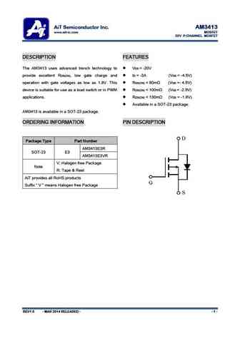
am3413.pdf
AiT Semiconductor Inc. AM3413 www.ait-ic.com MOSFET 20V P-CHANNEL MOSFET DESCRIPTION FEATURES The AM3413 uses advanced trench technology to V = -20V DS provide excellent R , low gate charge and I = -3A (V = -4.5V) DS(ON) D GS operation with gate voltages as low as 1.8V. This R
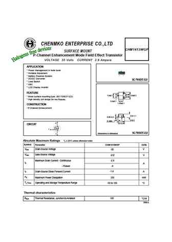
chm1413wgp.pdf
CHENMKO ENTERPRISE CO.,LTD CHM1413WGP SURFACE MOUNT P-Channel Enhancement Mode Field Effect Transistor VOLTAGE 20 Volts CURRENT 2.9 Ampere APPLICATION * Power Management in Note book * Portable Equipment * Battery Powered System * DC/DC Converter SC-70/SOT-323 * Load Switch * DSC * LCD Display inverter FEATURE 0.65 1.3 0.1 2.0 0.2 * Small surface mounting type. (SC-70/S
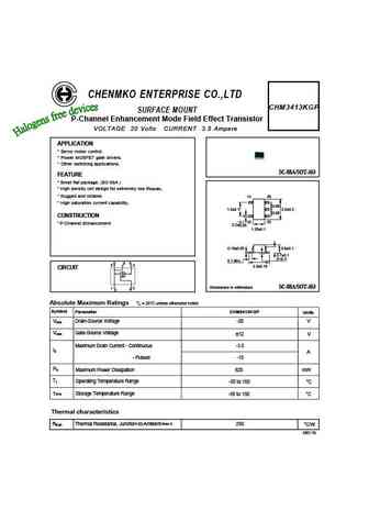
chm3413kgp.pdf
CHENMKO ENTERPRISE CO.,LTD CHM3413KGP SURFACE MOUNT P-Channel Enhancement Mode Field Effect Transistor VOLTAGE 20 Volts CURRENT 3.5 Ampere APPLICATION * Servo motor control. * Power MOSFET gate drivers. * Other switching applications. SC-88A/SOT-353 FEATURE * Small flat package. (SC-88A ) * High density cell design for extremely low RDS(ON). * Rugged and reliable. (1) (5) * Hi
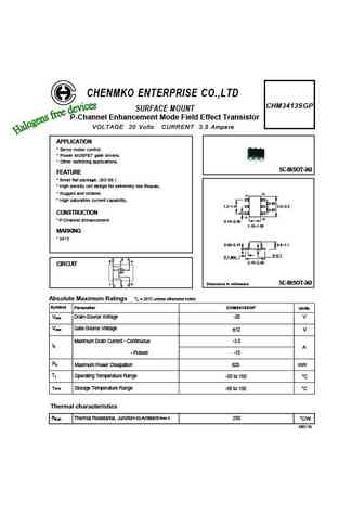
chm3413sgp.pdf
CHENMKO ENTERPRISE CO.,LTD CHM3413SGP SURFACE MOUNT P-Channel Enhancement Mode Field Effect Transistor VOLTAGE 20 Volts CURRENT 3.5 Ampere APPLICATION * Servo motor control. * Power MOSFET gate drivers. * Other switching applications. SC-88/SOT-363 FEATURE * Small flat package. (SC-88 ) * High density cell design for extremely low RDS(ON). * Rugged and reliable. (6) (1) * Hig
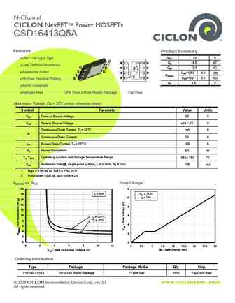
csd16413q5a.pdf
N-Channel CICLON NexFET Power MOSFETs CSD16413Q5A Features Product Summary Ultra Low Qg & Qgd VDS 25 V D S 1 8 D S 1 8 D Qg 9.0 nC Low Thermal Resistance D S 2 7 D G S 2 7 D Qgd 2.5 nC D Avalanche Rated S D S 3 6 D S 3 6 D VGS=4.5V 4.1 m S RDS(on) D D G 4 5 D G 4 5 D VGS=10V 3.1 m Pb Free Terminal Plating S Vth 1.6 V RoHS Complian
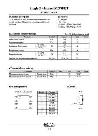
elm34413aa-n.pdf
Single P-channel MOSFET ELM34413AA-N General description Features ELM34413AA-N uses advanced trench technology to Vds=-30V provide excellent Rds(on), low gate charge and low gate Id=-12A resistance. Rds(on)
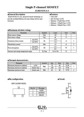
elm13413ca.pdf
Single P-channel MOSFET ELM13413CA-S General description Features ELM13413CA-S uses advanced trench technology to Vds=-20V provide excellent Rds(on), low gate charge and low gate Id=-3A (Vgs=-4.5V) resistance. Rds(on)
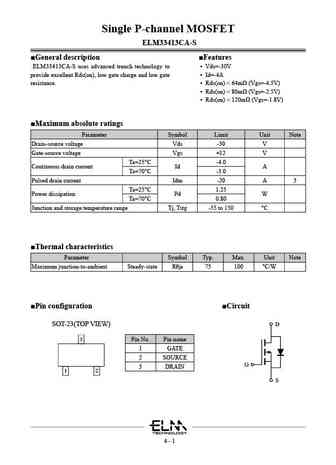
elm33413ca.pdf
Single P-channel MOSFET ELM33413CA-S General description Features ELM33413CA-S uses advanced trench technology to Vds=-30V provide excellent Rds(on), low gate charge and low gate Id=-4A resistance. Rds(on)
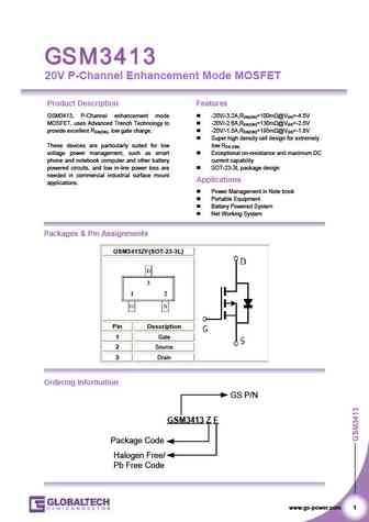
gsm3413.pdf
20V P-Channel Enhancement Mode MOSFET Product Description Features GSM3413, P-Channel enhancement mode -20V/-3.2A,RDS(ON)=100m @VGS=-4.5V MOSFET, uses Advanced Trench Technology to -20V/-2.6A,RDS(ON)=130m @VGS=-2.5V provide excellent RDS(ON), low gate charge. -20V/-1.5A,RDS(ON)=195m @VGS=-1.8V Super high density cell design for extremely These devices are particularly su
gsm3413a.pdf
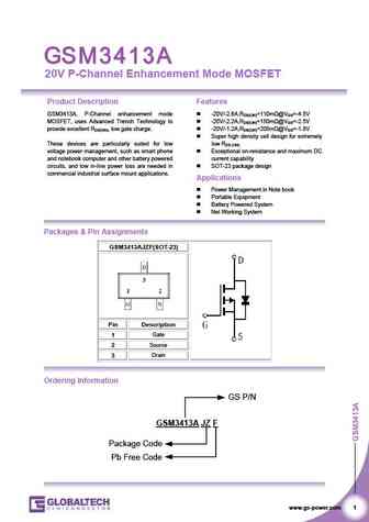
20V P-Channel Enhancement Mode MOSFET Product Description Features GSM3413A, P-Channel enhancement mode -20V/-2.6A,RDS(ON)=110m @VGS=-4.5V MOSFET, uses Advanced Trench Technology to -20V/-2.2A,RDS(ON)=150m @VGS=-2.5V provide excellent RDS(ON), low gate charge. -20V/-1.2A,RDS(ON)=205m @VGS=-1.8V Super high density cell design for extremely These devices are par
gsm1413.pdf
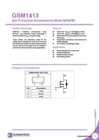
GSM1413 20V P-Channel Enhancement Mode MOSFET Product Description Features GSM1413, P-Channel enhancement mode -20V/-3.0A , RDS(ON)= 125m @VGS=-4.5V MOSFET, uses Advanced Trench Technology to -20V/-2.4A , RDS(ON)= 160m @VGS=-2.5V provide excellent RDS(ON), low gate charge. Super high density cell design for extremely low RDS (ON) These devices are particularly sui
gsm4134w.pdf
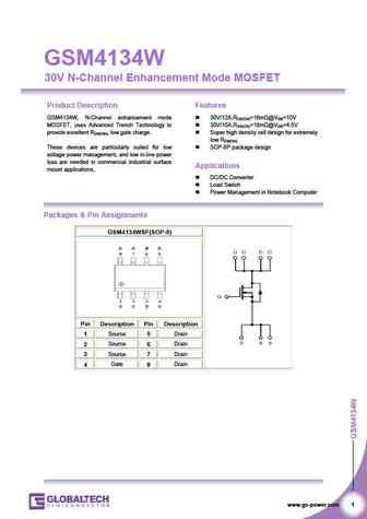
GSM4134W 30V N-Channel Enhancement Mode MOSFET Product Description Features GSM4134W, N-Channel enhancement mode 30V/12A,RDS(ON)=16m @VGS=10V MOSFET, uses Advanced Trench Technology to 30V/10A,RDS(ON)=18m @VGS=4.5V provide excellent RDS(ON), low gate charge. Super high density cell design for extremely low RDS(ON) These devices are particularly suited for low SOP-8P pac
gsm4134.pdf
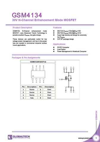
30V N-Channel Enhancement Mode MOSFET Product Description Features GSM4134, N-Channel enhancement mode 30V/12A,RDS(ON)=15m @VGS=10V MOSFET, uses Advanced Trench Technology to 30V/10A,RDS(ON)=20m @VGS=4.5V provide excellent RDS(ON), low gate charge. Super high density cell design for extremely low RDS(ON) These devices are particularly suited for low SOP-8P package design
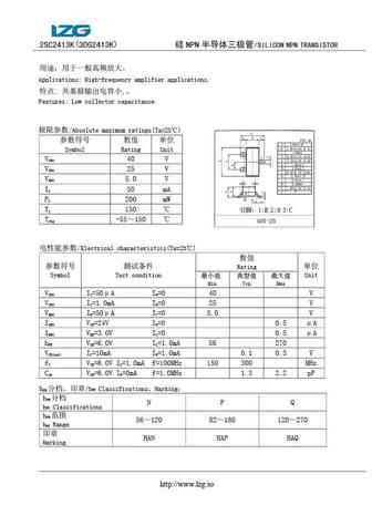
3dg2413k.pdf
2SC2413K(3DG2413K) NPN /SILICON NPN TRANSISTOR Applications High-frequency amplifier applications. , Features Low collector capacitance. /Absolute maximum ratings(Ta=25 ) Symbol Rating Unit V 40 V CBO V 25 V CEO V 5.0 V EBO I 50 mA
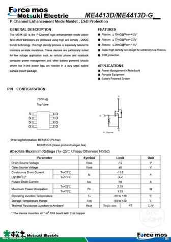
me4413d me4413d-g.pdf
ME4413D/ME4413D-G P-Channel Enhancement Mode Mosfet , ESD Protection GENERAL DESCRIPTION FEATURES RDS(ON) 13m @VGS=-4.5V The ME4413D is the P-Channel logic enhancement mode power RDS(ON) 17m @VGS=-2.5V field effect transistors are produced using high cell density , DMOS RDS(ON) 26m @VGS=-1.8V trench technology. This high density process is especially tailo
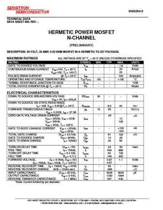
shd226413.pdf
SENSITRON SHD226413 SEMICONDUCTOR TECHNICAL DATA DATA SHEET 686, REV. - HERMETIC POWER MOSFET N-CHANNEL (PRELIMINARY) DESCRIPTION 30 VOLT, 20 AMP, 0.02 OHM MOSFET IN A HERMETIC TO-257 PACKAGE. MAXIMUM RATINGS ALL RATINGS ARE AT TA = 25 C UNLESS OTHERWISE SPECIFIED. RATING SYMBOL MIN. TYP. MAX. UNITS GATE TO SOURCE VOLTAGE VGS - - 15 Volts ID - - 20 Amps CONTINUOUS DRAIN CUR
shd225413.pdf
SENSITRON SHD225413 SEMICONDUCTOR TECHNICAL DATA DATA SHEET 693, REV. - HERMETIC POWER MOSFET N-CHANNEL (PRELIMINARY) DESCRIPTION 30 VOLT, 35 AMP, 0.012 OHM MOSFET IN A HERMETIC TO-254 PACKAGE. MAXIMUM RATINGS ALL RATINGS ARE AT TA = 25 C UNLESS OTHERWISE SPECIFIED. RATING SYMBOL MIN. TYP. MAX. UNITS GATE TO SOURCE VOLTAGE VGS - - 15 Volts ID - - 35 Amps CONTINUOUS DRAIN CU
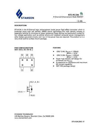
stp1413a.pdf
ST1413A P Channel Enhancement Mode MOSFET -3.4A DESCRIPTION ST1413A is the P-Channel logic enhancement mode power field effect transistor which is produced using high cell density, DMOS trench technology.This high density process is especially tailored to minimize on-state resistance.These devices are particularly suited for low voltage application such as cellular phone and not
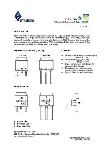
stp413d.pdf
STP413D P Channel Enhancement Mode MOSFET -12.0A DESCRIPTION STP413D is the P-Channel logic enhancement mode power field effect transistor which is produced using high cell density, DMOS trench technology. The STP413D has been designed specially to improve the overall efficiency of DC/DC converters using either synchronous or conventional switching PWM controllers. It has been o
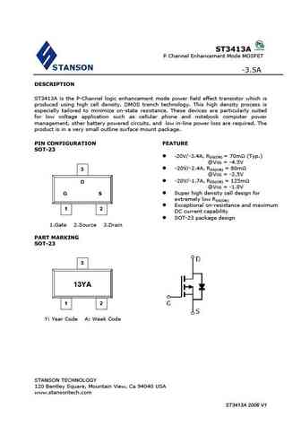
st3413a.pdf
ST3413A P Channel Enhancement Mode MOSFET -3.5A DESCRIPTION ST3413A is the P-Channel logic enhancement mode power field effect transistor which is produced using high cell density, DMOS trench technology. This high density process is especially tailored to minimize on-state resistance. These devices are particularly suited for low voltage application such as cellular phone and n
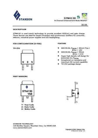
stn4130.pdf
STN4130 N Channel Enhancement Mode MOSFET 30.0A DESCRIPTION STN4130 is used trench technology to provide excellent RDS(on) and gate charge. Those devices are ideal for boost converters and synchronous rectifiers for consumer, telecom, industrial power supplies and LED backlighting. FEATURE PIN CONFIGURATION (D-PAK) 60V/20.0A, RDS(ON) = 40m (Typ.) TO-252 @VGS = 10V 6
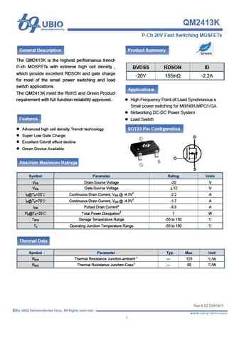
qm2413k.pdf
QM2413K P-Ch 20V Fast Switching MOSFETs General Description Product Summery The QM2413K is the highest performance trench P-ch MOSFETs with extreme high cell density , BVDSS RDSON ID which provide excellent RDSON and gate charge -20V 155m -2.2A for most of the small power switching and load switch applications. Applications The QM2413K meet the RoHS and Green Product req
qm2413v.pdf
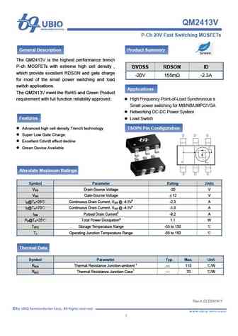
QM2413V P-Ch 20V Fast Switching MOSFETs General Description Product Summery The QM2413V is the highest performance trench P-ch MOSFETs with extreme high cell density , BVDSS RDSON ID which provide excellent RDSON and gate charge -20V 155m -2.3A for most of the small power switching and load switch applications. Applications The QM2413V meet the RoHS and Green Product req
ao3413a.pdf
R UMW UMW AO3413A 20V P-Channel MOSFET SOT 23 General Description General Description The AO3413 uses advanced trench technology to The AO3413 uses advanced trench technology to provide excellent RDS(ON), low gate charge and provide excellent RDS(ON), low gate charge and operation with gate voltages as low as 1.8V. This operation with gate voltages as low as 1.8V. This device
fmmt413.pdf
FMMT413 SOT23 NPN silicon planar avalanche transistor Summary V(BR)CES = 150V, V(BR)CEO = 50V, IUSB = 25A Description The FMMT413 is a NPN silicon planar bipolar transistor optimized for avalanche mode operation. Tight process control and low inductance packaging combine to produce high current pulses with fast edges, ideal for laser diode driving. Features C Avalanche mode opera
lpm3413.pdf
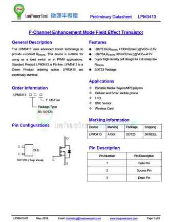
Preliminary Datasheet LPM3413 P-Channel Enhancement Mode Field Effect Transistor General Description Features The LPM3413 uses advanced trench technology to -20V/2.0A,R 130m (max.)@VGS=-2.5V DS(ON) provide excellent R . This device is suitable for -20V/3A,R 95m (max.)@VGS=-4.5V DS(ON) DS(ON) using as a load switch or in PWM applications. Super high density cell
ao3413.pdf
AO3413 P-Channel Enhancement Mode MOSFET Feature DS(ON) GS -20V/-3A, R = 120m (MAX) @V = -4.5V. DS(ON) GS R = 150m (MAX) @V = -2.5V. DS(ON) Super High dense cell design for extremely low R 3 Reliable and Rugged SC-59 for Surface Mount Package SC-59 1 2 Applications 1 Gate 2 Source 3 Drain Power Management Portable Equipment and Battery Powered Sy
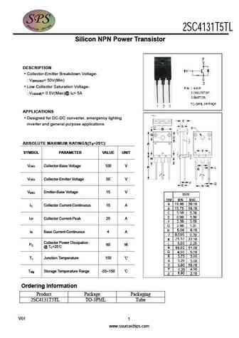
2sc4131t5tl.pdf
2SC4131T5TL Silicon NPN Power Transistor DESCRIPTION Collector-Emitter Breakdown Voltage- V = 50V(Min) (BR)CEO Low Collector Saturation Voltage- V = 0.5V(Max)@ I = 5A CE(sat) C APPLICATIONS Designed for DC-DC converter, emergency lighting inverter and general purpose applications ABSOLUTE MAXIMUM RATINGS(T =25 ) a SYMBOL PARAMETER VALUE UNIT V Collector-Base Voltage 1
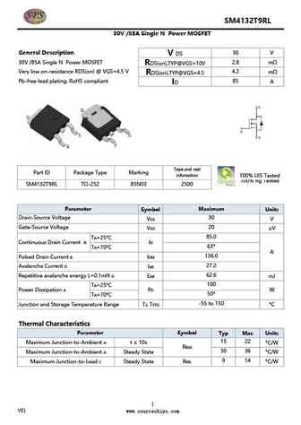
sm4132t9rl.pdf
SM4132T9RL 30V /85A Single N Power MOSFET H N03H N 30V /85A Single N Power MOSFET 85N03H General Description 30 V V DS 30V /85A Single N Power MOSFET 2.8 m RDS(on),TYP@VGS=10V Very low on-resistance RDS(on) @ VGS=4.5 V 4.2 m RDS(on),TYP@VGS=4.5 Pb-free lead plating; RoHS compliant 85 A ID Tape and reel Part ID Package Type Marking infomation 100% UIS Tested 100% Rg Tested S
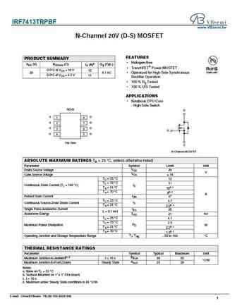
irf7413trpbf.pdf
IRF7413TRPBF www.VBsemi.tw N-Channel 20V (D-S) MOSFET FEATURES PRODUCT SUMMARY Halogen-free VDS (V) RDS(on) ( ) ID (A)a Qg (Typ.) TrenchFET Power MOSFET 0.012 at VGS = 10 V 12 20 6.1 nC Optimized for High-Side Synchronous 0.015 at VGS = 4.5 V 11 Rectifier Operation 100 % Rg Tested 100 % UIS Tested APPLICATIONS Notebook CPU Core - High-Side Switch
ntp6413ang.pdf
NTP6413ANG www.VBsemi.tw N-Channel 100-V (D-S) MOSFET FEATURES PRODUCT SUMMARY TrenchFET Power MOSFETS V(BR)DSS (V) rDS(on) ( )ID (A) Available 175 C Junction Temperature 0.032 at VGS = 10 V 45 RoHS* 100 Low Thermal Resistance Package 0.035 at VGS = 4.5 V 40 COMPLIANT D TO-220AB G S G D S Top View N-Channel MOSFET ABSOLUTE MAXIMUM RATINGS TC = 25 C,
stp413d.pdf
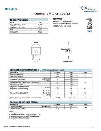
STP413D www.VBsemi.tw P-Channel 4 0 V (D-S) MOSFET FEATURES PRODUCT SUMMARY TrenchFET power MOSFET VDS (V) -40 Package with low thermal resistance RDS(on) ( ) at VGS = -10 V 0.012 100 % Rg and UIS tested RDS(on) ( ) at VGS = -4.5 V 0.015 ID (A) -50 Configuration Single TO-252 S G D D G S P-Channel MOSFET Top View ABSOLUTE MAXIMUM RATINGS (TC = 25 C, unle
aod4132.pdf
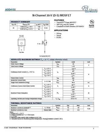
AOD4132 www.VBsemi.tw N-Channel 30-V (D-S) MOSFET FEATURES PRODUCT SUMMARY TrenchFET Power MOSFET VDS (V) RDS(on) ( ) ID (A)a, e Qg (Typ) 100 % Rg and UIS Tested Compliant to RoHS Directive 2011/65/EU 0.002 at VGS = 10 V 100 30 72 nC 0.003 at VGS = 4.5 V 90 APPLICATIONS D OR-ing Server TO-252 DC/DC G G D S Top View S N-Channel MOSFET ABSOL
st3413a.pdf
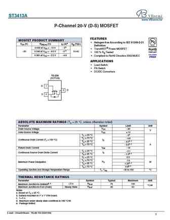
ST3413A www.VBsemi.tw P-Channel 20-V (D-S) MOSFET FEATURES MOSFET PRODUCT SUMMARY Halogen-free According to IEC 61249-2-21 VDS (V) RDS(on) ( )ID (A)a Qg (Typ.) Definition 0.035 at VGS = - 10 V - 5e TrenchFET Power MOSFET e - 20 0.043 at VGS = - 4.5 V - 5 10 nC 100 % Rg Tested 0.061 at VGS = - 2.5 V - 4.8 Compliant to RoHS Directive 2002/95/EC APPLICATIONS
aod4130.pdf
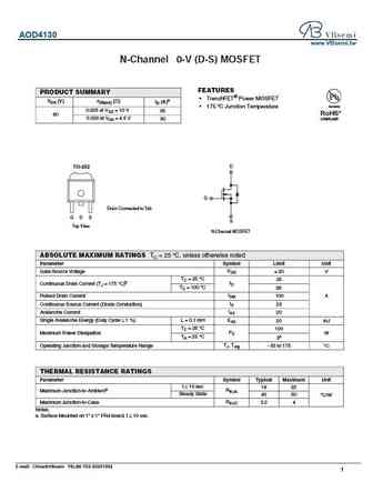
AOD4130 www.VBsemi.tw N-Channel 6 0-V (D-S) MOSFET FEATURES PRODUCT SUMMARY TrenchFET Power MOSFET VDS (V) rDS(on) ( ) ID (A)a Available 175 C Junction Temperature 0.025 at VGS = 10 V 35 RoHS* 60 0.030 at VGS = 4.5 V 30 COMPLIANT TO-252 D G Drain Connected to Tab G D S S Top View N-Channel MOSFET ABSOLUTE MAXIMUM RATINGS TC = 25 C, unless otherwise noted
hm3413b.pdf
HM3413B P-Channel Enhancement Mode Power MOSFET DESCRIPTION D The HM3413B uses advanced trench technology to provide excellent RDS(ON), low gate charge and operation with gate G voltages as low as 2.5V. This device is suitable for use as a load switch or in PWM applications. S GENERAL FEATURES Schematic diagram VDS = -20V,ID = -3A RDS(ON)
hm3413.pdf
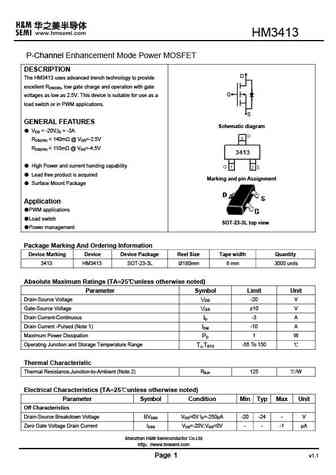
HM3413 P-Channel Enhancement Mode Power MOSFET DESCRIPTION D The HM3413 uses advanced trench technology to provide excellent RDS(ON), low gate charge and operation with gate G voltages as low as 2.5V. This device is suitable for use as a load switch or in PWM applications. S GENERAL FEATURES Schematic diagram VDS = -20V,ID = -3A RDS(ON)
2sc4131.pdf
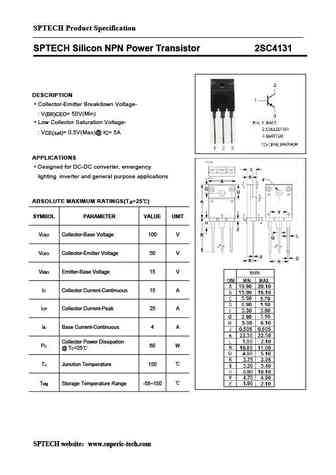
SPTECH Product Specification SPTECH Silicon NPN Power Transistor 2SC4131 DESCRIPTION Collector-Emitter Breakdown Voltage- V = 50V(Min) (BR)CEO Low Collector Saturation Voltage- VCE(sat)= 0.5V(Max)@ IC= 5A APPLICATIONS Designed for DC-DC converter, emergency lighting inverter and general purpose applications ABSOLUTE MAXIMUM RATINGS(Ta=25 ) SYMBOL PARAMETER VALUE UNIT VC
2sc4134.pdf
isc Silicon NPN Power Transistor 2SC4134 DESCRIPTION High voltage and large current capacity Fast-speed switching Small and slim package permitting 2SC4134-applied sets to be made more compact 100% avalanche tested Minimum Lot-to-Lot variations for robust device performance and reliable operation APPLICATIONS Power supplies,relay drivers,lamp drivers ABSOLUTE MAXIMUM RATIN
2sa1413-z.pdf
isc Silicon PNP Power Transistor 2SA1413-Z DESCRIPTION With TO-252(DPAK) packaging Large collector current Low collector saturation voltage High power dissipation Minimum Lot-to-Lot variations for robust device performance and reliable operation APPLICATIONS Designed for use in DC-DC converter Driver of solenoid or motor ABSOLUTE MAXIMUM RATINGS(T =25 ) a SYMBOL PAR
2sd1413.pdf
isc Silicon NPN Darlington Power Transistor 2SD1413 DESCRIPTION Collector-Emitter Breakdown Voltage- V = 40V(Min) (BR)CEO Collector-Emitter Saturation Voltage- V = 1.5V(Max) @I = 2A CE(sat) C High DC Current Gain h = 2000(Min) @ I = 1A, V = 2V FE C CE Complement to Type 2SB1023 Minimum Lot-to-Lot variations for robust device performance and reliable operation APPLI
2sc4139.pdf
isc Silicon NPN Power Transistor 2SC4139 DESCRIPTION High Collector-Emitter Breakdown Voltage- V = 400V(Min) (BR)CEO High Switching Speed High Reliability Minimum Lot-to-Lot variations for robust device performance and reliable operation APPLICATIONS Designed for switching regulator and general purpose applications. ABSOLUTE MAXIMUM RATINGS(T =25 ) a SYMBOL PARAMETER
2sc1413a.pdf
INCHANGE Semiconductor isc Silicon NPN Power Transistor 2SC1413A DESCRIPTION High Collector-base breakdown voltage 1500V Low saturation voltage@5A Large area of safe operation Minimum Lot-to-Lot variations for robust device performance and reliable operation APPLICATIONS Designed for the horizontal output stage in power-transformer-less television receivers. ABSOLUTE MAXIMU
aod413a.pdf
isc P-Channel MOSFET Transistor AOD413A FEATURES Drain Current I = -12A@ T =25 D C Drain Source Voltage- V =-40V(Min) DSS Static Drain-Source On-Resistance R =11m (Max) DS(on) 100% avalanche tested Minimum Lot-to-Lot variations for robust device performance and reliable operation DESCRIPTION Designed for use in switch mode power supplies and general purpose
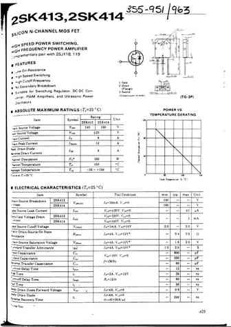
2sk413.pdf
isc N-Channel MOSFET Transistor 2SK413 DESCRIPTION Drain Current I = 8A@ T =25 D C Drain Source Voltage- V = 140V(Min) DSS Fast Switching Speed 100% avalanche tested Minimum Lot-to-Lot variations for robust device performance and reliable operation APPLICATIONS High speed switching. High Cutoff frequency. No secondary breakdown. Suitable for switching re
2sk3413ls.pdf
isc N-Channel MOSFET Transistor 2SK3413LS FEATURES Drain Current I = 25A@ T =25 D C Drain Source Voltage V = 60V(Min) DSS Static Drain-Source On-Resistance R = 33m (Max) @ V = 10V DS(on) GS 100% avalanche tested Minimum Lot-to-Lot variations for robust device performance and reliable operation DESCRIPTION motor drive, DC-DC converter, power switch and soleno
irfb4137.pdf
isc N-Channel MOSFET Transistor IRFB4137 IIRFB4137 FEATURES Static drain-source on-resistance RDS(on) 69m Enhancement mode Fast Switching Speed 100% avalanche tested Minimum Lot-to-Lot variations for robust device performance and reliable operation DESCRITION High Efficiency Synchronous Rectification in SMPS Uninterruptible Power Supply ABSOLUTE MAXIMUM
irfp4137.pdf
isc N-Channel MOSFET Transistor IRFP4137 IIRFP4137 FEATURES Static drain-source on-resistance RDS(on) 69m Enhancement mode 100% avalanche tested Minimum Lot-to-Lot variations for robust device performance and reliable operation DESCRITION High Speed Power Switching ABSOLUTE MAXIMUM RATINGS(T =25 ) a SYMBOL PARAMETER VALUE UNIT V Drain-Source Voltage 300 V
2sc4138.pdf
isc Silicon NPN Power Transistor 2SC4138 DESCRIPTION High Collector-Emitter Breakdown Voltage- V = 400V(Min) (BR)CEO High Switching Speed High Reliability Minimum Lot-to-Lot variations for robust device performance and reliable operation APPLICATIONS Designed for switching regulator and general purpose applications. ABSOLUTE MAXIMUM RATINGS(T =25 ) a SYMBOL PARAMETER
aod4132.pdf
isc N-Channel MOSFET Transistor AOD4132 FEATURES Drain Current I = 85A@ T =25 D C Drain Source Voltage- V =30V(Min) DSS Static Drain-Source On-Resistance R =4.0m (Max) DS(on) 100% avalanche tested Minimum Lot-to-Lot variations for robust device performance and reliable operation DESCRIPTION Designed for use in switch mode power supplies and general purpose
2sc4130.pdf
isc Silicon NPN Power Transistor 2SC4130 DESCRIPTION Collector-Emitter Breakdown Voltage- V = 400V(Min) (BR)CEO High Switching Speed Minimum Lot-to-Lot variations for robust device performance and reliable operation APPLICATIONS Designed for switching regulator and general purpose applications. ABSOLUTE MAXIMUM RATINGS(T =25 ) a SYMBOL PARAMETER VALUE UNIT V Collector-
2sc4131.pdf
isc Silicon NPN Power Transistor 2SC4131 DESCRIPTION Collector-Emitter Breakdown Voltage- V = 50V(Min) (BR)CEO Low Collector Saturation Voltage- V = 0.5V(Max)@ I = 5A CE(sat) C Minimum Lot-to-Lot variations for robust device performance and reliable operation APPLICATIONS Designed for DC-DC converter, emergency lighting inverter and general purpose applications ABSOLUTE
aod4136.pdf
isc N-Channel MOSFET Transistor AOD4136 FEATURES Drain Current I = 25A@ T =25 D C Drain Source Voltage- V =25V(Min) DSS Static Drain-Source On-Resistance R =11m (Max) DS(on) 100% avalanche tested Minimum Lot-to-Lot variations for robust device performance and reliable operation DESCRIPTION Designed for use in switch mode power supplies and general purpose a
aod4130.pdf
INCHANGE Semiconductor Isc N-Channel MOSFET Transistor AOD4130 FEATURES With To-252(DPAK) package Low input capacitance and gate charge Low gate input resistance 100% avalanche tested Minimum Lot-to-Lot variations for robust device performance and reliable operation APPLICATIONS Switching applications Load switch Power management ABSOLUTE MAXIMUM RATINGS(T =25
2sc4135.pdf
isc Silicon NPN Power Transistor 2SC4135 DESCRIPTION High breakdown voltage and large current capacity Fast switching speed Small and slim package 100% avalanche tested Minimum Lot-to-Lot variations for robust device performance and reliable operation Complementary to 2SA1593 APPLICATIONS Power supplies, relay drivers,lamp drivers. ABSOLUTE MAXIMUM RATINGS(T =25 ) a
irlb4132.pdf
INCHANGE Semiconductor isc N-Channel MOSFET Transistor IRLB4132 FEATURES With low gate drive requirements Easy to drive 100% avalanche tested Minimum Lot-to-Lot variations for robust device performance and reliable operation APPLICATIONS Switching applications Low voltage power tools ABSOLUTE MAXIMUM RATINGS(T =25 ) a SYMBOL PARAMETER VALUE UNIT V Drain-Source
2sc1413.pdf
Inchange Semiconductor Product Specification Silicon NPN Power Transistors 2SC1413 DESCRIPTION With TO-3 package High voltage ,high speed APPLICATIONS For TV horizontal deflection output applications PINNING(see fig.2) PIN DESCRIPTION 1 Base 2 Emitter Fig.1 simplified outline (TO-3) and symbol 3 Collector Absolute maximum ratings(Ta= ) SYMBOL PARAMETER CONDI
mj413.pdf
isc Silicon NPN Power Transistor MJ413 DESCRIPTION High Collector-Emitter Sustaining Voltage- V = 325V(Min.) CEO(SUS) DC Current Gain- h = 20-80@ I = 0.5A FE C Minimum Lot-to-Lot variations for robust device performance and reliable operation APPLICATIONS Designed for medium to high voltage inverters, converters, regulators and switching circuits. ABSOLUTE MAXIMUM RATIN
aoi4130.pdf
Isc N-Channel MOSFET Transistor AOI4130 FEATURES With TO-251(IPAK) package Low input capacitance and gate charge Low gate input resistance 100% avalanche tested Minimum Lot-to-Lot variations for robust device performance and reliable operation APPLICATIONS Switching applications Load switch Power management ABSOLUTE MAXIMUM RATINGS(T =25 ) a SYMBOL PARAMETE
Другие транзисторы: 41026, 41027, 41028, 41038, 41039, 41042, 41044, 411, SS8050, 41500, 41501, 41502, 41503, 41504, 41505, 41506, 41508
History: 40911
🌐 : EN ES РУ
Список транзисторов
Обновления
BJT: GA1A4M | SBT42 | 2SA200-Y | 2SA200-O | 2SD882-Q | 2SD882-P | 2SD882-E | 2SC945-L | 2SC945-H | 2SC4226-R23 | 2SC3357-F | 2SC3357-E | 2SC3356-R26 | 2SC3356-R24 | 2SC3356-R23 | 2SB772-Q | 2SB772-P | 2SB772-E | 2SA1015-L | 2SA1015-H | HSS8550
Popular searches
fgpf4636 datasheet | 2sc1945 | c2383 | 2sb681 | bc639 equivalent | bd138 transistor equivalent | c1096 transistor | c1345 transistor
