2N3052 datasheet, аналоги, основные параметры
Наименование производителя: 2N3052 📄📄
Тип материала: Si
Полярность: NPN
Предельные значения
Максимальная рассеиваемая мощность (Pc): 0.35 W
Макcимально допустимое напряжение коллектор-база (Ucb): 35 V
Макcимально допустимое напряжение коллектор-эмиттер (Uce): 15 V
Макcимально допустимое напряжение эмиттер-база (Ueb): 5 V
Макcимальный постоянный ток коллектора (Ic): 0.03 A
Предельная температура PN-перехода (Tj): 200 °C
Электрические характеристики
Граничная частота коэффициента передачи тока (ft): 40 MHz
Ёмкость коллекторного перехода (Cc): 5 pf
Статический коэффициент передачи тока (hFE): 25
Корпус транзистора: 610A-03
📄📄 Копировать
Аналоги (замена) для 2N3052
- подборⓘ биполярного транзистора по параметрам
2N3052 даташит
2n3055a mj2955a mj15015 mj15016.pdf
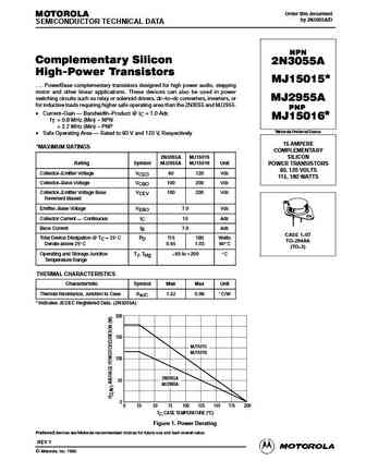
Order this document MOTOROLA by 2N3055A/D SEMICONDUCTOR TECHNICAL DATA NPN Complementary Silicon 2N3055A High-Power Transistors * MJ15015 . . . PowerBase complementary transistors designed for high power audio, stepping motor and other linear applications. These devices can also be used in power switching circuits such as relay or solenoid drivers, dc to dc converters, inverters
mj2955-2n3055.pdf

Order this document MOTOROLA by 2N3055/D SEMICONDUCTOR TECHNICAL DATA NPN 2N3055 * Complementary Silicon Power PNP MJ2955* Transistors . . . designed for general purpose switching and amplifier applications. *Motorola Preferred Device DC Current Gain hFE = 20 70 @ IC = 4 Adc Collector Emitter Saturation Voltage 15 AMPERE VCE(sat) = 1.1 Vdc (Max) @ IC = 4 Adc P
2n3055 mj2955.pdf
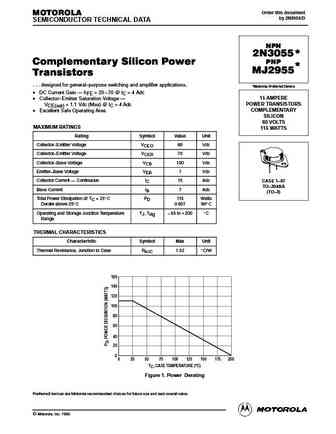
Order this document MOTOROLA by 2N3055/D SEMICONDUCTOR TECHNICAL DATA NPN 2N3055 * Complementary Silicon Power PNP MJ2955* Transistors . . . designed for general purpose switching and amplifier applications. *Motorola Preferred Device DC Current Gain hFE = 20 70 @ IC = 4 Adc Collector Emitter Saturation Voltage 15 AMPERE VCE(sat) = 1.1 Vdc (Max) @ IC = 4 Adc P
2n3055.pdf
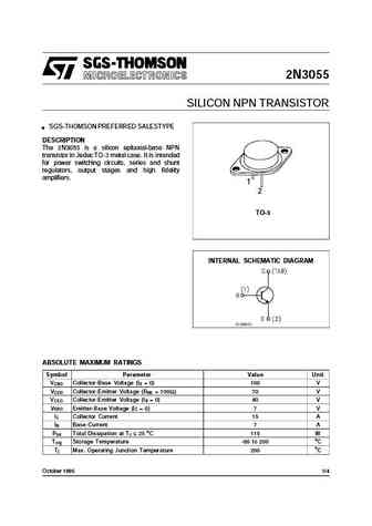
2N3055 SILICON NPN TRANSISTOR n SGS-THOMSON PREFERRED SALESTYPE DESCRIPTION The 2N3055 is a silicon epitaxial-base NPN transistor in Jedec TO-3 metal case. It is intended for power switching circuits, series and shunt regulators, output stages and high fidelity amplifiers. 1 2 TO-3 INTERNAL SCHEMATIC DIAGRAM ABSOLUTE MAXIMUM RATINGS Symbol Parameter Value Unit VCBO Collector-Base
2n3055 mj2955 2.pdf
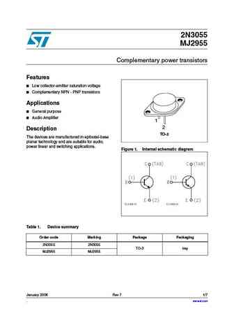
2N3055 MJ2955 Complementary power transistors Features Low collector-emitter saturation voltage Complementary NPN - PNP transistors Applications General purpose Audio Amplifier 1 2 Description TO-3 The devices are manufactured in epitaxial-base planar technology and are suitable for audio, power linear and switching applications. Figure 1. Internal schematic d
2n3053-a.pdf
145 Adams Avenue, Hauppauge, NY 11788 USA Tel (631) 435-1110 Fax (631) 435-1824
2n3054-a 2n3054.pdf
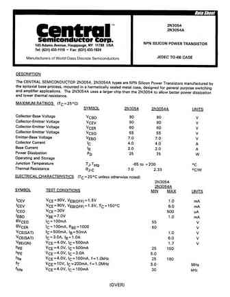
145 Adams Avenue, Hauppauge, NY 11788 USA Tel (631) 435-1110 Fax (631) 435-1824
2n3055a mj15015 mj15016.pdf

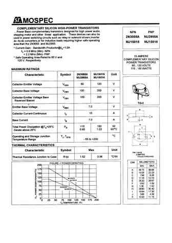
2N3055A (NPN), MJ15015 (NPN), MJ15016 (PNP) MJ15015 and MJ15016 are Preferred Devices Complementary Silicon High-Power Transistors http //onsemi.com These PowerBaset complementary transistors are designed for high power audio, stepping motor and other linear applications. These 15 AMPERE devices can also be used in power switching circuits such as relay or solenoid drivers, dc-to-dc
2n3055g.pdf

2N3055(NPN), MJ2955(PNP) Preferred Device Complementary Silicon Power Transistors Complementary silicon power transistors are designed for general-purpose switching and amplifier applications. Features http //onsemi.com DC Current Gain - hFE = 20-70 @ IC = 4 Adc Collector-Emitter Saturation Voltage - 15 AMPERE VCE(sat) = 1.1 Vdc (Max) @ IC = 4 Adc POWER TRANSISTORS Exc
2n3055ag.pdf
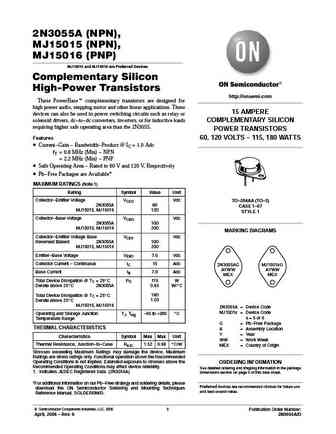
2N3055A (NPN), MJ15015 (NPN), MJ15016 (PNP) MJ15015 and MJ15016 are Preferred Devices Complementary Silicon High-Power Transistors http //onsemi.com These PowerBaset complementary transistors are designed for high power audio, stepping motor and other linear applications. These 15 AMPERE devices can also be used in power switching circuits such as relay or solenoid drivers, dc-to-dc
2n3055ag mj15015g mj15016g.pdf
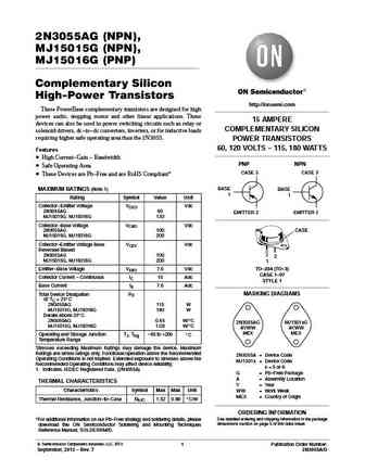
2N3055AG (NPN), MJ15015G (NPN), MJ15016G (PNP) Complementary Silicon High-Power Transistors http //onsemi.com These PowerBase complementary transistors are designed for high power audio, stepping motor and other linear applications. These 15 AMPERE devices can also be used in power switching circuits such as relay or COMPLEMENTARY SILICON solenoid drivers, dc-to-dc converters, invert
2n3055 mj2955.pdf
2N3055(NPN), MJ2955(PNP) Preferred Device Complementary Silicon Power Transistors Complementary silicon power transistors are designed for general-purpose switching and amplifier applications. Features http //onsemi.com DC Current Gain - hFE = 20-70 @ IC = 4 Adc Collector-Emitter Saturation Voltage - 15 AMPERE VCE(sat) = 1.1 Vdc (Max) @ IC = 4 Adc POWER TRANSISTORS Exc
2n3055.pdf
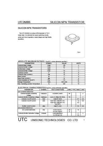
UTC 2N3055 SILICON NPN TRANSISTOR SILICON NPN TRANSISTORS The UTC 2N3055 is a silicon NPN transistor in TO-3 metal case. It is intended for power switching circuits, series and shunt regulators, output stages and high fidelity amplifiers. TO-3 ABSOLUTE MAXIMUM RATINGS ( Ta=25 C ,unless otherwise specified ) PARAMETERS SYMBOL VALUE UNITS Collector-Base Voltage VCBO 100 V Collector-Em
2n3055esmd.pdf
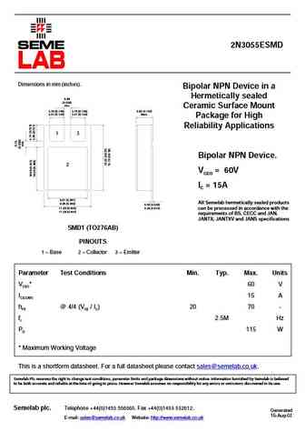
2N3055ESMD Dimensions in mm (inches). Bipolar NPN Device in a Hermetically sealed 0.89 (0.035) min. Ceramic Surface Mount 3.70 (0.146) 3.70 (0.146) 3.60 (0.142) 3.41 (0.134) 3.41 (0.134) Max. Package for High Reliability Applications 1 3 Bipolar NPN Device. 2 VCEO = 60V IC = 15A 9.67 (0.381) All Semelab hermetically sealed products 9.38 (0.369) 0.50 (0.020) 0.26
2n3053smd.pdf

2N3053SMD Dimensions in mm (inches). Bipolar NPN Device in a Hermetically sealed 0.89 (0.035) min. Ceramic Surface Mount 3.70 (0.146) 3.70 (0.146) 3.60 (0.142) 3.41 (0.134) 3.41 (0.134) Max. Package for High Reliability Applications 1 3 Bipolar NPN Device. 2 VCEO = 40V IC = 0.7A 9.67 (0.381) All Semelab hermetically sealed products 9.38 (0.369) 0.50 (0.020) 0.26
2n3053smd05.pdf
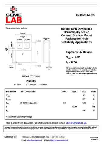
2N3053SMD05 Dimensions in mm (inches). Bipolar NPN Device in a Hermetically sealed 7.54 (0.296) 0.76 (0.030) Ceramic Surface Mount min. 3.175 (0.125) 2.41 (0.095) Package for High 2.41 (0.095) Max. 0.127 (0.005) Reliability Applications 1 3 Bipolar NPN Device. 2 VCEO = 40V IC = 0.7A 0.127 (0.005) 16 PLCS 0.127 (0.005) 0.50(0.020) 0.50 (0.020) All Semelab he
2n3053 a.pdf
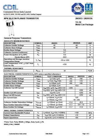
Continental Device India Limited An ISO/TS 16949, ISO 9001 and ISO 14001 Certified Company NPN SILICON PLANAR TRANSISTOR 2N3053 / 2N3053A TO-39 Metal Can Package General Purpose Transistors ABSOLUTE MAXIMUM RATINGS DESCRIPTION SYMBOL 2N3053 2N3053A UNIT Collector Emitter Voltage VCEO 40 60 V Collector Base Voltage VCBO 60 80 V Emitter Base Voltage VEBO 5.0 V Collector Current Continu
2n3055hv.pdf
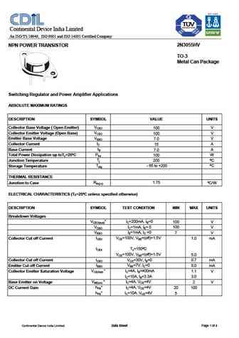
Continental Device India Limited An ISO/TS 16949, ISO 9001 and ISO 14001 Certified Company 2N3055HV NPN POWER TRANSISTOR TO-3 Metal Can Package Switching Regulator and Power Amplifier Applications ABSOLUTE MAXIMUM RATINGS DESCRIPTION SYMBOL VALUE UNITS VCBO Collector Base Voltage ( Open Emitter) V 100 VCEO Collector Emitter Voltage (Open Base) V 100 VEBO Emitter Base Voltage V
2n3055 mj2955.pdf
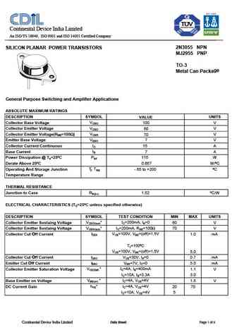
Continental Device India Limited An ISO/TS 16949, ISO 9001 and ISO 14001 Certified Company 2N3055 NPN SILICON PLANAR POWER TRANSISTORS MJ2955 PNP TO-3 Metal Can Package General Purpose Switching and Amplifier Applications ABSOLUTE MAXIMUM RATINGS DESCRIPTION SYMBOL UNITS VALUE Collector Base Voltage VCBO V 100 Collector Emitter Voltage VCEO V 60 Collector Emitter Voltage(RBE=100
2n3055.pdf
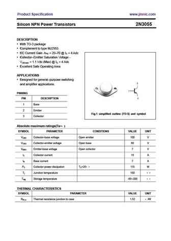
Product Specification www.jmnic.com Silicon NPN Power Transistors 2N3055 DESCRIPTION With TO-3 package Complement to type MJ2955 DC Current Gain -hFE = 20 70 @ IC = 4 Adc Collector Emitter Saturation Voltage - VCE(sat) = 1.1 Vdc (Max) @ IC = 4 Adc Excellent Safe Operating Area APPLICATIONS Designed for general purpose switching and amplifier applications.
2n3019 2n3057 2n3700.pdf
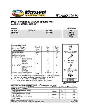
TECHNICAL DATA LOW POWER NPN SILICON TRANSISTOR Qualified per MIL-PRF-19500/391 Devices Qualified Level 2N3019 2N3057A 2N3700 JAN 2N3019S 2N3700S JANTX JANTXV JANS MAXIMUM RATINGS Ratings Symbol Value Units Collector-Emitter Voltage 80 Vdc VCEO Collector-Base Voltage 140 Vdc VCBO TO-39* (TO-205AD) Emitter-Base Voltage 7.0 Vdc VEBO 2N3019, 2N3019S Collector
2n3055.pdf
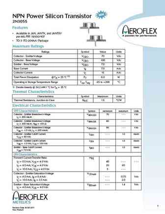
NPN Power Silicon Transistor 2N3055 Features Available in JAN, JANTX, and JANTXV per MIL-PRF-19500/407 TO-3 (TO-204AA) Package Maximum Ratings Ratings Symbol Value Units Collector - Emitter Voltage VCEO 70 Vdc Collector - Base Voltage VCBO 100 Vdc Emitter - Base Voltage VEBO 7.0 Vdc Base Current IB 7.0 Adc Collector Current IC 15 Adc Total Power Dissipation @ TA = 25 C (
2n3055.pdf
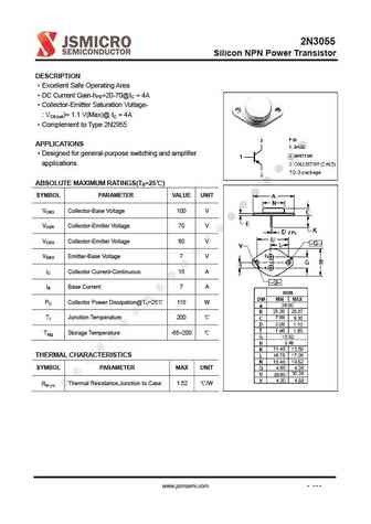
2N3055 Silicon NPN Power Transistor DESCRIPTION Excellent Safe Operating Area DC Current Gain-hFE=20-70@IC = 4A Collector-Emitter Saturation Voltage- VCE(sat)= 1.1 V(Max)@ IC = 4A Complement to Type 2N2955 APPLICATIONS Designed for general-purpose switching and amplifier applications ABSOLUTE MAXIMUM RATINGS(Ta=25 ) SYMBOL PARAMETER VALUE UNIT VCBO Collecto
2n3055t3bl.pdf
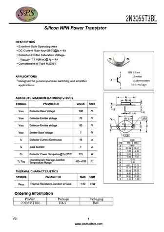
2N3055T3BL Silicon NPN Power Transistor DESCRIPTION Excellent Safe Operating Area DC Current Gain-h =20-70@I = 4A FE C Collector-Emitter Saturation Voltage- V )= 1.1 V(Max)@ I = 4A CE(sat C Complement to Type MJ2955 APPLICATIONS Designed for general-purpose switching and amplifier applications ABSOLUTE MAXIMUM RATINGS(T =25 ) a SYMBOL PARAMETER VALUE UNIT V Collect
2n3055.pdf
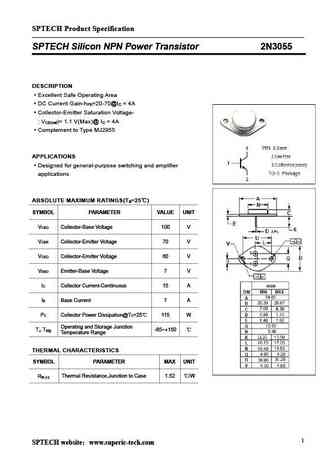
SPTECH Product Specification SPTECH Silicon NPN Power Transistor 2N3055 DESCRIPTION Excellent Safe Operating Area DC Current Gain-h =20-70@I = 4A FE C Collector-Emitter Saturation Voltage- V )= 1.1 V(Max)@ I = 4A CE(sat C Complement to Type MJ2955 APPLICATIONS Designed for general-purpose switching and amplifier applications ABSOLUTE MAXIMUM RATINGS(T =25 ) a SYMBOL
2n3054 2n3054a.pdf
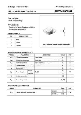
Inchange Semiconductor Product Specification Silicon NPN Power Transistors 2N3054 2N3054A DESCRIPTION With TO-66 package APPLICATIONS Designed for general purpose switching and amplifier applications PINNING (See Fig.2) PIN DESCRIPTION 1 Base 2 Emitter Fig.1 simplified outline (TO-66) and symbol 3 Collector Absolute maximum ratings(Ta=25 ) SYMBOL PARAMETER CONDITI
2n3055a.pdf
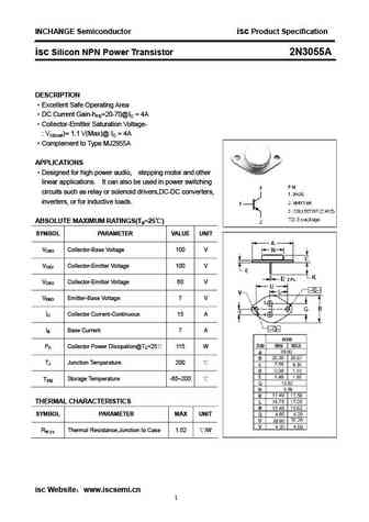
INCHANGE Semiconductor isc Product Specification isc Silicon NPN Power Transistor 2N3055A DESCRIPTION Excellent Safe Operating Area DC Current Gain-hFE=20-70@IC = 4A Collector-Emitter Saturation Voltage- VCE(sat)= 1.1 V(Max)@ IC = 4A Complement to Type MJ2955A APPLICATIONS Designed for high power audio, stepping motor and other linear applications. It can also be
2n3055.pdf

isc Silicon NPN Power Transistor 2N3055 DESCRIPTION Excellent Safe Operating Area DC Current Gain-h =20-70@I = 4A FE C Collector-Emitter Saturation Voltage- V )= 1.1 V(Max)@ I = 4A CE(sat C Complement to Type MJ2955 Minimum Lot-to-Lot variations for robust device performance and reliable operation APPLICATIONS Designed for general-purpose switching and amplifier appli
2n3054.pdf
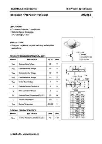
INCHANGE Semiconductor isc Product Specification isc Silicon NPN Power Transistor 2N3054 DESCRIPTION Continuous Collector Current-IC= 4A Collector Power Dissipation- PC= 25W @TC= 25 APPLICATIONS Designed for general purpose switching and amplifier applications. ABSOLUTE MAXIMUM RATINGS(Ta=25 ) SYMBOL PARAMETER VALUE UNIT VCBO Collector-Base Voltage 90 V V C
2n3055h.pdf
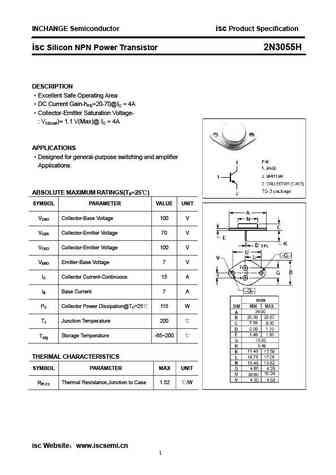
INCHANGE Semiconductor isc Product Specification isc Silicon NPN Power Transistor 2N3055H DESCRIPTION Excellent Safe Operating Area DC Current Gain-hFE=20-70@IC = 4A Collector-Emitter Saturation Voltage- VCE(sat)= 1.1 V(Max)@ IC = 4A APPLICATIONS Designed for general-purpose switching and amplifier Applications. ABSOLUTE MAXIMUM RATINGS(Ta=25 ) SYMBOL PARAMETER
2n3055b.pdf
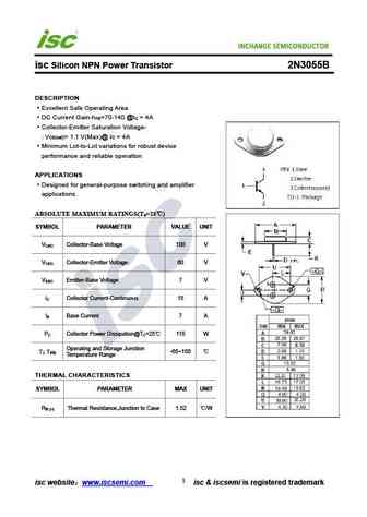
isc Silicon NPN Power Transistor 2N3055B DESCRIPTION Excellent Safe Operating Area DC Current Gain-h =70-140 @I = 4A FE C Collector-Emitter Saturation Voltage- V )= 1.1 V(Max)@ I = 4A CE(sat C Minimum Lot-to-Lot variations for robust device performance and reliable operation APPLICATIONS Designed for general-purpose switching and amplifier applications ABSOLUTE MAXIMUM
Другие транзисторы: 2N3044, 2N3045, 2N3046, 2N3047, 2N3048, 2N3049, 2N3050, 2N3051, 2SC2655, 2N3053, 2N3053A, 2N3053L, 2N3053S, 2N3053SM, 2N3054, 2N3054A, 2N3054S
Параметры биполярного транзистора и их взаимосвязь

Список транзисторов
Обновления
BJT: ZDT6705 | GA1L4Z | GA1A4M | SBT42 | 2SA200-Y | 2SA200-O | 2SD882-Q | 2SD882-P | 2SD882-E | 2SC945-L | 2SC945-H | 2SC4226-R23 | 2SC3357-F | 2SC3357-E | 2SC3356-R26 | 2SC3356-R24 | 2SC3356-R23 | 2SB772-Q | 2SB772-P | 2SB772-E | 2SA1015-L
Popular searches
toshiba 2sc2290 | pk6d0ba mosfet | 2sd726 | c536 transistor equivalent | 2sa1294 datasheet | mp10b transistor | bc182b | 2n3054 transistor equivalent