C450. Аналоги и основные параметры
Наименование производителя: C450
Тип материала: Si
Полярность: NPN
Предельные значения
Максимальная рассеиваемая мощность (Pc): 0.2 W
Макcимально допустимое напряжение коллектор-база (Ucb): 40 V
Макcимально допустимое напряжение коллектор-эмиттер (Uce): 40 V
Макcимально допустимое напряжение эмиттер-база (Ueb): 5 V
Предельная температура PN-перехода (Tj): 125 °C
Электрические характеристики
Граничная частота коэффициента передачи тока (ft): 60 MHz
Ёмкость коллекторного перехода (Cc): 6 pf
Статический коэффициент передачи тока (hFE): 100
Корпус транзистора: TO106
Аналоги (замена) для C450
- подборⓘ биполярного транзистора по параметрам
C450 даташит
0.1. Size:122K 1
ntmfs5c450nlt3g.pdf 
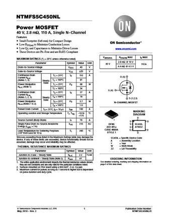
NTMFS5C450NL Power MOSFET 40 V, 2.8 mW, 110 A, Single N-Channel Features Small Footprint (5x6 mm) for Compact Design Low RDS(on) to Minimize Conduction Losses Low QG and Capacitance to Minimize Driver Losses www.onsemi.com These Devices are Pb-Free and are RoHS Compliant V(BR)DSS RDS(ON) MAX ID MAX MAXIMUM RATINGS (TJ = 25 C unless otherwise noted) 2.8 mW @ 10 V Par
0.2. Size:169K 1
ntmfs5c450nt3g.pdf 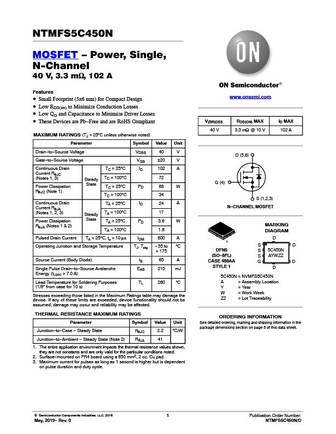
NTMFS5C450N MOSFET Power, Single, N-Channel 40 V, 3.3 mW, 102 A Features www.onsemi.com Small Footprint (5x6 mm) for Compact Design Low RDS(on) to Minimize Conduction Losses Low QG and Capacitance to Minimize Driver Losses V(BR)DSS RDS(ON) MAX ID MAX These Devices are Pb-Free and are RoHS Compliant 40 V 3.3 mW @ 10 V 102 A MAXIMUM RATINGS (TJ = 25 C unless other
0.3. Size:243K motorola
bc450rev.pdf 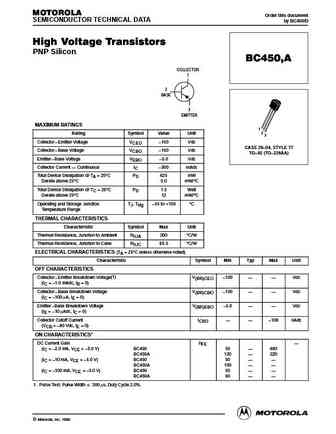
MOTOROLA Order this document SEMICONDUCTOR TECHNICAL DATA by BC450/D High Voltage Transistors PNP Silicon BC450,A COLLECTOR 1 2 BASE 3 EMITTER MAXIMUM RATINGS 1 2 Rating Symbol Value Unit 3 Collector Emitter Voltage VCEO 100 Vdc CASE 29 04, STYLE 17 Collector Base Voltage VCBO 100 Vdc TO 92 (TO 226AA) Emitter Base Voltage VEBO 5.0 Vdc Collector Curren
0.4. Size:83K sanyo
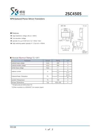
2sc4504.pdf 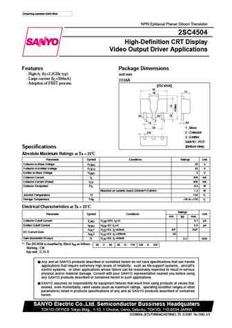
Ordering number EN3160A NPN Epitaxial Planar Silicon Transistor 2SC4504 High-Definition CRT Display Video Output Driver Applications Features Package Dimensions High fT (fT=2.2GHz typ) unit mm Large current (IC=300mA) 2038A Adoption of FBET process. [2SC4504] 4.5 1.5 1.6 0.4 0.5 3 2 1 0.4 1.5 3.0 1 Base 2 Collector 0.75 3 Emitter SANYO PCP (Bottom vi
0.6. Size:160K onsemi
nvmfs5c450nl.pdf 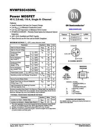
NVMFS5C450NL Power MOSFET 40 V, 2.8 mW, 110 A, Single N-Channel Features Small Footprint (5x6 mm) for Compact Design Low RDS(on) to Minimize Conduction Losses www.onsemi.com Low QG and Capacitance to Minimize Driver Losses NVMFS5C450NLWF - Wettable Flank Option for Enhanced Optical Inspection V(BR)DSS RDS(ON) MAX ID MAX AEC-Q101 Qualified and PPAP Capable 2.8 mW
0.7. Size:122K onsemi
ntmfs5c450nl.pdf 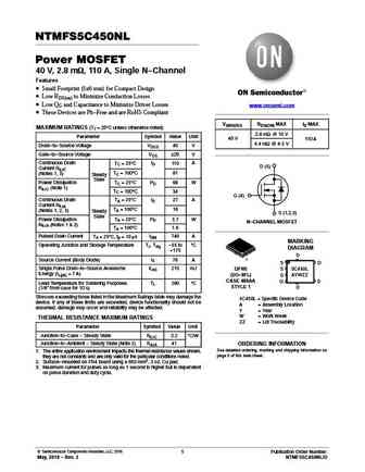
NTMFS5C450NL Power MOSFET 40 V, 2.8 mW, 110 A, Single N-Channel Features Small Footprint (5x6 mm) for Compact Design Low RDS(on) to Minimize Conduction Losses Low QG and Capacitance to Minimize Driver Losses www.onsemi.com These Devices are Pb-Free and are RoHS Compliant V(BR)DSS RDS(ON) MAX ID MAX MAXIMUM RATINGS (TJ = 25 C unless otherwise noted) 2.8 mW @ 10 V Par
0.8. Size:169K onsemi
ntmfs5c450n.pdf 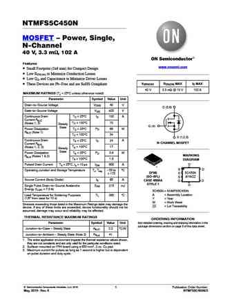
NTMFS5C450N MOSFET Power, Single, N-Channel 40 V, 3.3 mW, 102 A Features www.onsemi.com Small Footprint (5x6 mm) for Compact Design Low RDS(on) to Minimize Conduction Losses Low QG and Capacitance to Minimize Driver Losses V(BR)DSS RDS(ON) MAX ID MAX These Devices are Pb-Free and are RoHS Compliant 40 V 3.3 mW @ 10 V 102 A MAXIMUM RATINGS (TJ = 25 C unless other
0.9. Size:166K onsemi
nvmfs5c450n.pdf 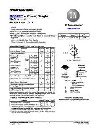
NVMFS5C450N MOSFET Power, Single N-Channel 40 V, 3.3 mW, 102 A Features www.onsemi.com Small Footprint (5x6 mm) for Compact Design Low RDS(on) to Minimize Conduction Losses Low QG and Capacitance to Minimize Driver Losses V(BR)DSS RDS(ON) MAX ID MAX NVMFS5C450NWF - Wettable Flank Option for Enhanced Optical 40 V 3.3 mW @ 10 V 102 A Inspection AEC-Q101 Qualif
0.10. Size:40K panasonic
2sc4502.pdf 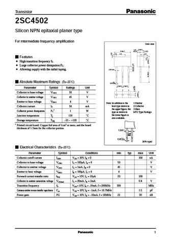
Transistor 2SC4502 Silicon NPN epitaxial planer type For mtermediate frequency amplification Unit mm 2.5 0.1 1.05 6.9 0.1 0.05 (1.45) 0.7 4.0 0.8 Features High transition frequency fT. Large collector power dissipation PC. 0.65 max. Allowing supply with the radial taping. +0.1 Absolute Maximum Ratings (Ta=25 C) 0.45 0.05 2.5 0.5 2.5 0.5 Parameter Symbol Rating
0.11. Size:45K panasonic
2sc4502 e.pdf 
Transistor 2SC4502 Silicon NPN epitaxial planer type For mtermediate frequency amplification Unit mm 2.5 0.1 1.05 6.9 0.1 0.05 (1.45) 0.7 4.0 0.8 Features High transition frequency fT. Large collector power dissipation PC. 0.65 max. Allowing supply with the radial taping. +0.1 Absolute Maximum Ratings (Ta=25 C) 0.45 0.05 2.5 0.5 2.5 0.5 Parameter Symbol Rating
0.12. Size:425K panasonic
dsc4501.pdf 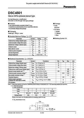
This product complies with the RoHS Directive (EU 2002/95/EC). DSC4501 Silicon NPN epitaxial planar type For low frequency amplification DSC2501 in NS through hole type package Features Package Low collector-emitter saturation voltage VCE(sat) Code Contributes to miniaturization of sets, mount area reduction NS-B2-B Eco-friendly Halogen-free package Pin N
0.13. Size:31K hitachi
2sc4501.pdf 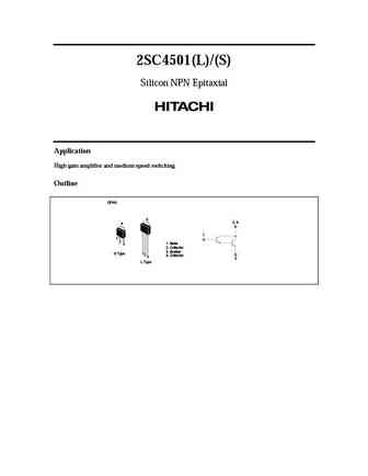
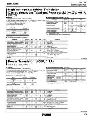
2SC4501(L)/(S) Silicon NPN Epitaxial Application High gain amplifier and medium speed switching Outline DPAK 4 2, 4 4 1 1 2 1. Base 3 2. Collector 3. Emitter S Type 12 4. Collector 3 3 L Type 2SC4501(L)/(S) Absolute Maximum Ratings (Ta = 25 C) Item Symbol Ratings Unit Collector to base voltage VCBO 30 V Collector to emitter voltage VCEO 30 V Emitter to base volta
0.14. Size:31K hitachi
2sc4500.pdf 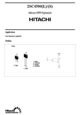
2SC4500(L)/(S) Silicon NPN Epitaxial Application Low frequency amplifier Outline DPAK 4 2, 4 4 1 1 2 1. Base 3 2. Collector 3. Emitter S Type 12 4. Collector 3 3 L Type 2SC4500(L)/(S) Absolute Maximum Ratings (Ta = 25 C) Item Symbol Ratings Unit Collector to base voltage VCBO 60 V Collector to emitter voltage VCEO 60 V Emitter to base voltage VEBO 7V Collector curr
0.15. Size:85K taiwansemi
tsc4505cx.pdf 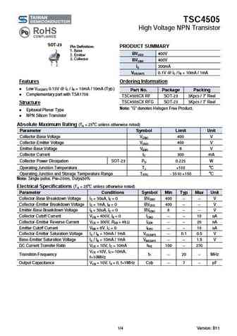
TSC4505 High Voltage NPN Transistor SOT-23 Pin Definition PRODUCT SUMMARY 1. Base BVCEO 400V 2. Emitter 3. Collector BVCBO 400V IC 300mA VCE(SAT) 0.1V @ IC / IB = 10mA / 1mA Features Ordering Information Low VCE(SAT) 0.15V @ IC / IB = 10mA / 10mA (Typ.) Part No. Package Packing Complementary part with TSA1759 TSC4505CX RF SOT-23 3Kpcs / 7 Reel TSC450
0.16. Size:134K cdil
bc446 bc448 bc450 a b.pdf 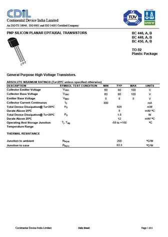
Continental Device India Limited An ISO/TS 16949, ISO 9001 and ISO 14001 Certified Company PNP SILICON PLANAR EPITAXIAL TRANSISTORS BC 446, A, B BC 448, A, B BC 450, A, B TO-92 Plastic Package General Purpose High Voltage Transistors. ABSOLUTE MAXIMUM RATINGS (Ta=25 C unless specified otherwise) DESCRIPTION SYMBOL TEST CONDITION MIN TYP MAX UNITS VCEO Collector Emitter Voltage 6
0.17. Size:142K jmnic
2sc4508.pdf 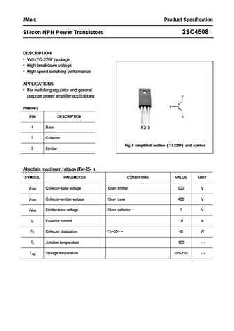
JMnic Product Specification Silicon NPN Power Transistors 2SC4508 DESCRIPTION With TO-220F package High breakdown voltage High speed switching performance APPLICATIONS For switching regulator and general purpose power amplifier applications PINNING PIN DESCRIPTION 1 Base 2 Collector Fig.1 simplified outline (TO-220F) and symbol 3 Emitter Absolute maximum rating
0.18. Size:225K jmnic
2sc4509.pdf 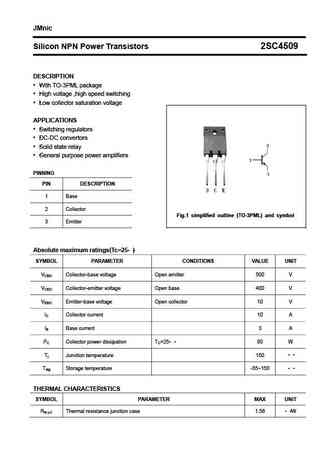
JMnic Silicon NPN Power Transistors 2SC4509 DESCRIPTION With TO-3PML package High voltage ,high speed switching Low collector saturation voltage APPLICATIONS Switching regulators DC-DC convertors Solid state relay General purpose power amplifiers PINNING PIN DESCRIPTION 1 Base 2 Collector Fig.1 simplified outline (TO-3PML) and symbol 3 Emitter Absolu
0.19. Size:142K jmnic
2sc4507.pdf 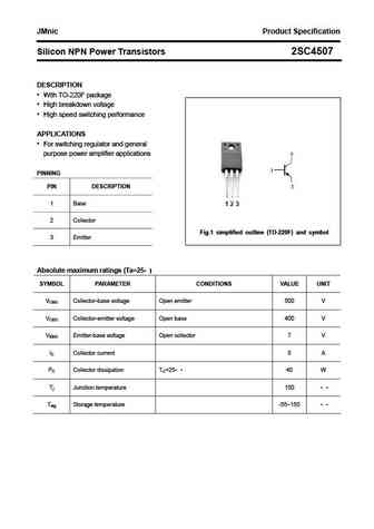
JMnic Product Specification Silicon NPN Power Transistors 2SC4507 DESCRIPTION With TO-220F package High breakdown voltage High speed switching performance APPLICATIONS For switching regulator and general purpose power amplifier applications PINNING PIN DESCRIPTION 1 Base 2 Collector Fig.1 simplified outline (TO-220F) and symbol 3 Emitter Absolute maximum rating
0.20. Size:415K wietron
wtc4501.pdf 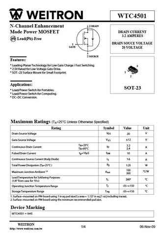
WTC4501 3 DRAIN N-Channel Enhancement DRAIN CURRENT Mode Power MOSFET 3.2 AMPERES P b Lead(Pb)-Free DRAIN SOUCE VOLTAGE 1 GATE 20 VOLTAGE 2 SOURCE Features * Leading Planar Technology for Low Gate Charge / Fast Switching. 3 * 2.5V Rated for Low Voltage Gate Drive. 1 * SOT-23 Surface Mount for Small Footprint. 2 Applications SOT-23 * Load/Power Switch for Portables. * Lo
0.21. Size:373K cystek
mtc4506q8.pdf 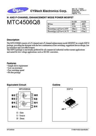
Spec. No. C780Q8 Issued Date 2012.05.17 CYStech Electronics Corp. Revised Date Page No. 1/12 N- AND P-CHANNEL ENHANCEMENT MODE POWER MOSFET N-CH P-CH MTC4506Q8 BVDSS 60V -60V ID 5.3A -3.9A RDSON(typ.) @VGS=(-)10V 28m 57m RDSON(typ.) @VGS=(-)4.5V 31m 67m Description The MTC4506Q8 consists of a N-channel and a P-channel enhancement-mode MOSFET in a single SO
0.22. Size:543K cystek
mtc4503q8g.pdf 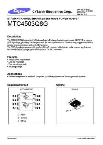
Spec. No. C384Q8 Issued Date 2010.12.10 CYStech Electronics Corp. Revised Date Page No. 1/10 N- AND P-CHANNEL ENHANCEMENT MODE POWER MOSFET MTC4503Q8G Description The MTC4503Q8G consists of a N-channel and a P-channel enhancement-mode MOSFET in a single SOP-8 package, providing the designer with the best combination of fast switching, ruggedized device design, low on
0.23. Size:763K cystek
mtc4503lq8.pdf 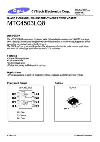
Spec. No. C384Q8 Issued Date 2015.01.06 CYStech Electronics Corp. Revised Date Page No. 1/10 N- AND P-CHANNEL ENHANCEMENT MODE POWER MOSFET MTC4503LQ8 Description The MTC4503LQ8 consists of a N-channel and a P-channel enhancement-mode MOSFET in a single SOP-8 package, providing the designer with the best combination of fast switching, ruggedized device design, low on
0.24. Size:520K cystek
mtc4505q8.pdf 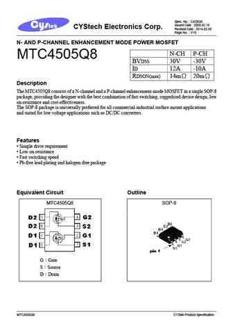
Spec. No. C439Q8 Issued Date 2009.02.19 CYStech Electronics Corp. Revised Date 2014.02.06 Page No. 1/10 N- AND P-CHANNEL ENHANCEMENT MODE POWER MOSFET N-CH P-CH MTC4505Q8 BVDSS 30V -30V ID 12A -10A RDSON(max) 14m 20m Description The MTC4505Q8 consists of a N-channel and a P-channel enhancement-mode MOSFET in a single SOP-8 package, providing the designer with t
0.25. Size:606K cystek
mtc4501q8.pdf 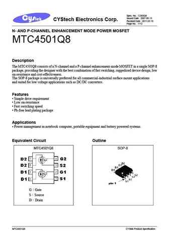
Spec. No. C385Q8 Issued Date 2007.06.13 CYStech Electronics Corp. Revised Date 2011.03.18 Page No. 1/12 N- AND P-CHANNEL ENHANCEMENT MODE POWER MOSFET MTC4501Q8 Description The MTC4501Q8 consists of a N-channel and a P-channel enhancement-mode MOSFET in a single SOP-8 package, providing the designer with the best combination of fast switching, ruggedized device design,
0.26. Size:775K cystek
mtc4503q8.pdf 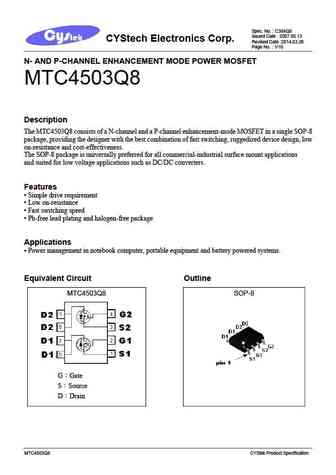
Spec. No. C384Q8 Issued Date 2007.06.13 CYStech Electronics Corp. Revised Date 2014.03.26 Page No. 1/10 N- AND P-CHANNEL ENHANCEMENT MODE POWER MOSFET MTC4503Q8 Description The MTC4503Q8 consists of a N-channel and a P-channel enhancement-mode MOSFET in a single SOP-8 package, providing the designer with the best combination of fast switching, ruggedized device design,
0.27. Size:180K cystek
btc4505m3.pdf 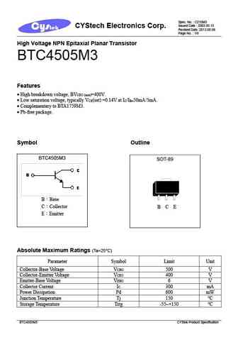
Spec. No. C210M3 Issued Date 2003.05.15 CYStech Electronics Corp. Revised Date 2013.08.06 Page No. 1/6 High Voltage NPN Epitaxial Planar Transistor BTC4505M3 Features High breakdown voltage, BV =400V. CEO (min) Low saturation voltage, typically V (sat) =0.14V at I /I 50mA/5mA. CE C B= Complementary to BTA1759M3. Pb-free package. Symbol Outline B
0.28. Size:355K cystek
mtc4506j4.pdf 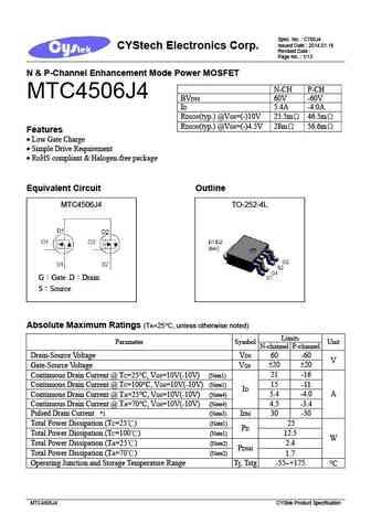
Spec. No. C780J4 Issued Date 2014.01.16 CYStech Electronics Corp. Revised Date Page No. 1/13 N & P-Channel Enhancement Mode Power MOSFET N-CH P-CH MTC4506J4 BVDSS 60V -60V ID 5.4A -4.0A RDSON(typ.) @VGS=(-)10V 25.5m 46.5m RDSON(typ.) @VGS=(-)4.5V 28m 56.6m Features Low Gate Charge Simple Drive Requirement RoHS compliant & Halogen-free packa
0.29. Size:422K cystek
mtc4503aq8.pdf 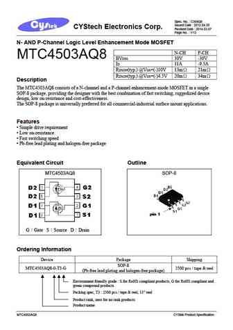
Spec. No. C384Q8 Issued Date 2012.04.30 CYStech Electronics Corp. Revised Date 2014.03.07 Page No. 1/12 N- AND P-Channel Logic Level Enhancement Mode MOSFET N-CH P-CH MTC4503AQ8 BVDSS 30V -30V ID 11A -9.5A RDSON(typ.) @VGS=(-)10V 13m 21m RDSON(typ.) @VGS=(-)4.5V 20m 34m Description The MTC4503AQ8 consists of a N-channel and a P-channel enhancement-mode MOS
0.30. Size:132K cystek
btc4505a3.pdf 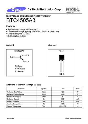
Spec. No. C210A3-R Issued Date 2003.10.15 CYStech Electronics Corp. Revised Date 2007.11.22 Page No. 1/4 High Voltage NPN Epitaxial Planar Transistor BTC4505A3 Features High breakdown voltage. (BV = 400V) CEO Low saturation voltage, typically V (sat) = 0.1V at I / I 10mA / 1mA. CE C B= Complementary to BTA1759A3 RoHS compliant package Symbol Outl
0.31. Size:245K cystek
btc4505n3.pdf 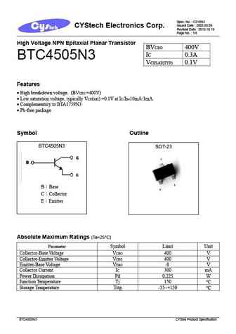
Spec. No. C210N3 Issued Date 2003.05.09 CYStech Electronics Corp. Revised Date 2010.10.19 Page No. 1/6 High Voltage NPN Epitaxial Planar Transistor BVCEO 400V IC 0.3A BTC4505N3 VCESAT(TYP) 0.1V Features High breakdown voltage. (BV =400V) CEO Low saturation voltage, typically V (sat) =0.1V at I /I 10mA/1mA. CE C B= Complementary to BTA1759N3 Pb-
0.32. Size:987K kexin
2sc4505.pdf 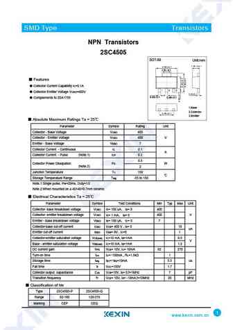
SMD Type Transistors NPN Transistors 2SC4505 SOT-89 Unit mm 1.70 0.1 Features Collector Current Capability IC=0.1A Collector Emitter Voltage VCEO=400V 0.42 0.1 0.46 0.1 Complements to 2SA1759 1.Base 2.Collector 3.Emitter Absolute Maximum Ratings Ta = 25 Parameter Symbol Rating Unit Collector - Base Voltage VCBO 400 Collector - Emitter Voltage VCEO 4
0.33. Size:1081K kexin
2sc4504.pdf 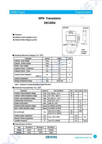
SMD Type Transistors NPN Transistors 2SC4504 SOT-89 Unit mm 1.70 0.1 Features Collector Current Capability IC=0.3A Collector Emitter Voltage VCEO=20V 0.42 0.1 0.46 0.1 1.Base 2.Collector 3.Emitter Absolute Maximum Ratings Ta = 25 Parameter Symbol Rating Unit Collector - Base Voltage VCBO 30 Collector - Emitter Voltage VCEO 20 V Emitter - Base Voltage VE
0.35. Size:180K inchange semiconductor
2sc4508.pdf 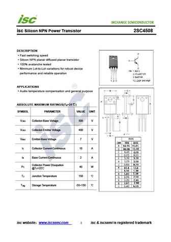
INCHANGE Semiconductor isc Silicon NPN Power Transistor 2SC4508 DESCRIPTION Fast switching speed Silicon NPN planar diffused planar transistor 100% avalanche tested Minimum Lot-to-Lot variations for robust device performance and reliable operation APPLICATIONS Audio temperature compensation and general purpose ABSOLUTE MAXIMUM RATINGS(T =25 ) a SYMBOL PARAMETER VALUE UNI
0.36. Size:190K inchange semiconductor
2sc4509.pdf 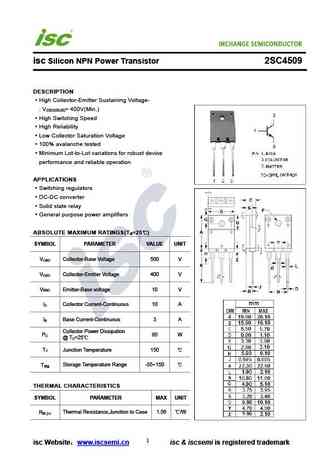
INCHANGE Semiconductor isc Silicon NPN Power Transistor 2SC4509 DESCRIPTION High Collector-Emitter Sustaining Voltage- V = 400V(Min.) CEO(SUS) High Switching Speed High Reliability Low Collector Saturation Voltage 100% avalanche tested Minimum Lot-to-Lot variations for robust device performance and reliable operation APPLICATIONS Switching regulators DC-DC conver
0.37. Size:180K inchange semiconductor
2sc4507.pdf 
INCHANGE Semiconductor isc Silicon NPN Power Transistor 2SC4507 DESCRIPTION Fast switching speed Silicon NPN planar diffused planar transistor 100% avalanche tested Minimum Lot-to-Lot variations for robust device performance and reliable operation APPLICATIONS Audio temperature compensation and general purpose ABSOLUTE MAXIMUM RATINGS(T =25 ) a SYMBOL PARAMETER VALUE UNI
Другие транзисторы: C420, C424, C425, C426, C428, C434, C441, C442, 2N2222, C5, C50-28, C5-8, C5-8Z, C5T2192, C5T2432, C5T2484, C5T2605