D100 datasheet, аналоги, основные параметры
Наименование производителя: D100 📄📄
Тип материала: Si
Полярность: NPN
Предельные значения
Максимальная рассеиваемая мощность (Pc): 0.5 W
Макcимально допустимое напряжение коллектор-база (Ucb): 60 V
Макcимально допустимое напряжение коллектор-эмиттер (Uce): 50 V
Макcимально допустимое напряжение эмиттер-база (Ueb): 1 V
Макcимальный постоянный ток коллектора (Ic): 1 A
Предельная температура PN-перехода (Tj): 150 °C
Электрические характеристики
Граничная частота коэффициента передачи тока (ft): 130 MHz
Статический коэффициент передачи тока (hFE): 50
Корпус транзистора: TO106
📄📄 Копировать
Аналоги (замена) для D100
- подборⓘ биполярного транзистора по параметрам
D100 даташит
c100 d100.pdf
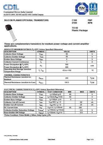
Continental Device India Limited An ISO/TS 16949, ISO 9001 and ISO 14001 Certified Company SILICON PLANAR EPITAXIAL TRANSISTORS C100 PNP D100 NPN TO-92 Plastic Package E CB These are complementary transistors for medium power voltage and current amplifier applications. ABSOLUTE MAXIMUM RATINGS (Ta=25 C Unless Specified Otherwise) DESCRIPTION SYMBOL VALUE UNITS VCBO Collector Base
std100n3lf3.pdf
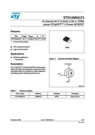
STD100N3LF3 N-channel 30 V, 0.0045 , 80 A, DPAK planar STripFET II Power MOSFET Features Type VDSSS RDS(on) ID Pw STD100N3LF3 30 V
std100nh03lt4.pdf
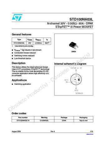
STD100NH03L N-channel 30V - 0.005 - 60A - DPAK STripFET III Power MOSFET General features VDSSS RDS(on) ID Type STD100NH03L 30V
stb100n10f7 std100n10f7 stf100n10f7 stf100n10f7 stp100n10f7.pdf
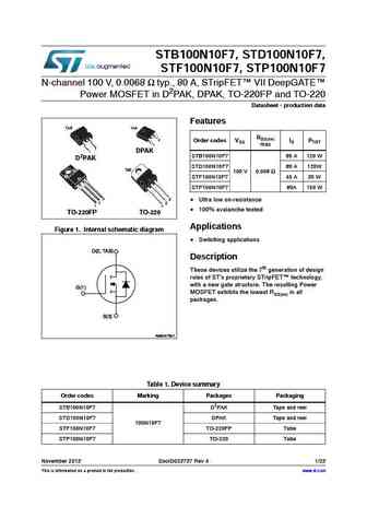
STB100N10F7, STD100N10F7, STF100N10F7, STP100N10F7 N-channel 100 V, 0.0068 typ., 80 A, STripFET VII DeepGATE Power MOSFET in D2PAK, DPAK, TO-220FP and TO-220 Datasheet - production data Features TAB TAB RDS(on) 3 Order codes VDS max ID PTOT 1 3 1 DPAK STB100N10F7 80 A 120 W D2PAK STD100N10F7 80 A 120W TAB 100 V 0.008 STF100N10F7 45 A 30 W STP100N10F7 80A 150 W
sgsd100-200.pdf
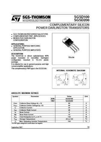
SGSD100 SGSD200 COMPLEMENTARY SILICON POWER DARLINGTON TRANSISTORS SGS-THOMSON PREFERRED SALESTYPES COMPLEMENTARY PNP - NPN DEVICES MONOLITHIC DARLINGTON CONFIGURATION APPLICATIONS GENERAL PURPOSE SWITCHING APPLICATION 3 GENERAL PURPOSE AMPLIFIERS 2 1 DESCRIPTION The SGSD100 is silicon epitaxial-base NPN TO-218 power transistor in monolithic Darlington configuration mou
2stbn15d100t4.pdf
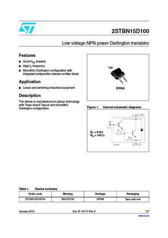
2STBN15D100 Low voltage NPN power Darlington transistor Features Good hFE linearity High fT frequency TAB Monolithic Darlington configuration with integrated antiparallel collector-emitter diode 3 Application 1 Linear and switching industrial equipment D PAK Description The device is manufactured in planar technology with base island layout and monolithic
2stbn15d100.pdf

2STBN15D100 Low voltage NPN power Darlington transistor Features Good hFE linearity High fT frequency TAB Monolithic Darlington configuration with integrated antiparallel collector-emitter diode 3 Application 1 Linear and switching industrial equipment D PAK Description The device is manufactured in planar technology with base island layout and monolithic
std100nh02l.pdf
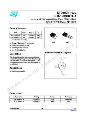
STD100NH02L STD100NH02L-1 N-channel 24V - 0.0042 - 60A - DPAK - IPAK STripFET II Power MOSFET General features VDSSS RDS(on) ID Type STD100NH02L 24V
stb100n10f7 std100n10f7 stf100n10f7 sti100n10f7 stp100n10f7.pdf
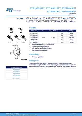
STB100N10F7, STD100N10F7, STF100N10F7 STI100N10F7, STP100N10F7 Datasheet N-channel 100 V, 6.8 m typ., 80 A STripFET F7 Power MOSFETs in D2PAK, DPAK, TO-220FP, I2PAK and TO-220 packages TAB TAB Features 2 3 1 VDS RDS(on) max. ID Order codes Package 3 1 D2PAK DPAK STB100N10F7 80 A D2PAK TAB TAB STD100N10F7 80 A DPAK STF100N10F7 100 V 8.0 m 45 A TO-220FP 3 3 2 3 1 2
std100n03lt4.pdf
STD100N03L STD100N03L-1 N-channel 30V - 0.0045 - 80A - DPAK - IPAK Planar STripFET II Power MOSFET General features VDSSS RDS(on) ID Type Pw STD100N03L 30 V
std100nh02lt4.pdf

STD100NH02L STD100NH02L-1 N-channel 24V - 0.0042 - 60A - DPAK - IPAK STripFET II Power MOSFET General features VDSSS RDS(on) ID Type STD100NH02L 24V
ftd1003.pdf
Ordering number ENN6428 P-Channel Silicon MOSFET FTD1003 Load Switching Applications Features Package Dimensions Low ON resistance. unit mm 2.5V drive. 2155A Mounting height 1.1mm. [FTD1003] Composite type, facilitating high-density mounting. 3.0 0.425 0.65 8 5 1 Drain1 2 Source1 1 4 3 Source1 0.125 4 Gate1 0.25 5 Gate2 6 Source2 7 Source2 8
rcd100n20.pdf
Data Sheet 10V Drive Nch MOSFET RCD100N20 Structure Dimensions (Unit mm) Silicon N-channel MOSFET CPT3 6.5 (SC-63) 5.1 2.3 0.5 Features 1) Low on-resistance. 2) High-speed switching. 0.75 3) Wide range of SOA. 0.65 0.9 2.3 (1) (2) (3) 4) Drive circuits can be simple. 2.3 0.5 1.0 5) Parallel use is easy. Application Switching Packaging spe
rsd100n10fra.pdf
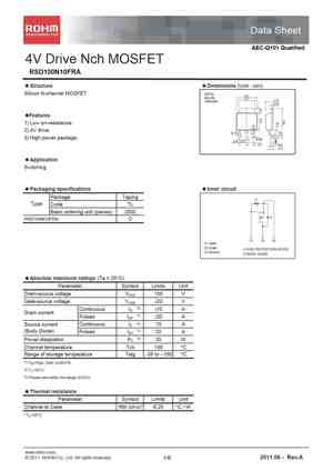
Data Sheet AEC-Q101 Qualified 4V Drive Nch MOSFET RSD100N10 RSD100N10FRA Structure Dimensions (Unit mm) Silicon N-channel MOSFET CPT3 6.5 (SC-63) 5.1 2.3 0.5 Features 1) Low on-resistance. 2) 4V drive. 0.75 3) High power package. 0.65 0.9 2.3 (1) (2) (3) 2.3 0.5 1.0 Application Switching Packaging specifications Inner circuit Packag
rcd100n19.pdf
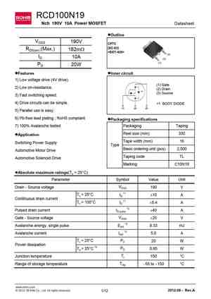
RCD100N19 Nch 190V 10A Power MOSFET Datasheet lOutline VDSS 190V CPT3 (SC-63) RDS(on) (Max.) 182mW (3) ID 10A (2) (1) PD 20W lFeatures lInner circuit 1) Low voltage drive (4V drive). (1) Gate 2) Low on-resistance. (2) Drain (3) Source 3) Fast switching speed. 4) Drive circuits can be simple. *1 BODY DIODE 5) Parallel use is easy. 6) Pb-free lead plat
rsd100n10.pdf
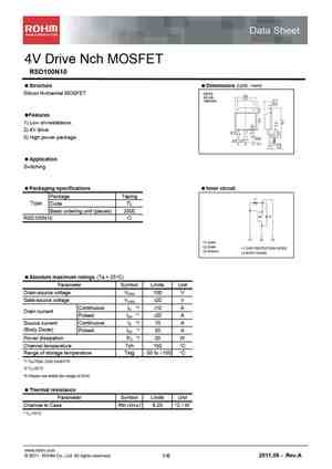
Data Sheet 4V Drive Nch MOSFET RSD100N10 Structure Dimensions (Unit mm) Silicon N-channel MOSFET CPT3 6.5 (SC-63) 5.1 2.3 0.5 Features 1) Low on-resistance. 2) 4V drive. 0.75 3) High power package. 0.65 0.9 2.3 (1) (2) (3) 2.3 0.5 1.0 Application Switching Packaging specifications Inner circuit Package Taping 1 Type Code TL Bas
sqd100n03-3m4.pdf
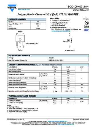
SQD100N03-3m4 www.vishay.com Vishay Siliconix Automotive N-Channel 30 V (D-S) 175 C MOSFET FEATURES PRODUCT SUMMARY TrenchFET Power MOSFET VDS (V) 30 100 % Rg and UIS Tested RDS(on) ( ) at VGS = 10 V 0.0034 AEC-Q101 Qualifiedd ID (A) 100 Material categorization Configuration Single For definitions of compliance please see www.vishay.com/doc?99912 TO-2
sqd100n04-3m6.pdf
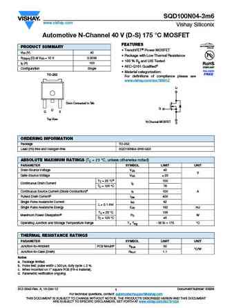
SQD100N04-3m6 www.vishay.com Vishay Siliconix Automotive N-Channel 40 V (D-S) 175 C MOSFET FEATURES PRODUCT SUMMARY TrenchFET Power MOSFET VDS (V) 40 Package with Low Thermal Resistance RDS(on) ( ) at VGS = 10 V 0.0036 100 % Rg and UIS Tested ID (A) 100 AEC-Q101 Qualifiedd Configuration Single Material categorization TO-252 For definitions of compli
sqd100n04-3m6l.pdf
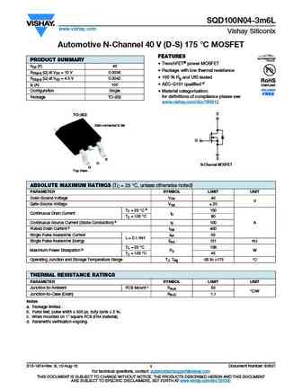
SQD100N04-3m6L www.vishay.com Vishay Siliconix Automotive N-Channel 40 V (D-S) 175 C MOSFET FEATURES PRODUCT SUMMARY TrenchFET power MOSFET VDS (V) 40 Package with low thermal resistance RDS(on) ( ) at VGS = 10 V 0.0036 100 % Rg and UIS tested RDS(on) ( ) at VGS = 4.5 V 0.0042 AEC-Q101 qualified d ID (A) 100 Configuration Single Material categorization
sqd100n03-3m2l.pdf
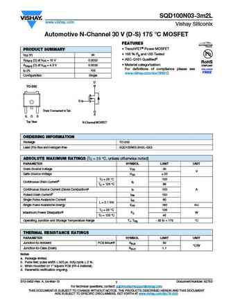
SQD100N03-3m2L www.vishay.com Vishay Siliconix Automotive N-Channel 30 V (D-S) 175 C MOSFET FEATURES TrenchFET Power MOSFET PRODUCT SUMMARY 100 % Rg and UIS Tested VDS (V) 30 AEC-Q101 Qualifiedd RDS(on) ( ) at VGS = 10 V 0.0032 Material categorization RDS(on) ( ) at VGS = 4.5 V 0.0039 For definitions of compliance please see ID (A) 100 www.vishay.com/doc?
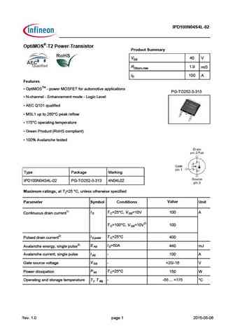
ipd100n04s4-02.pdf

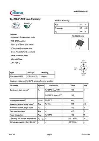
IPD100N04S4-02 OptiMOS -T2 Power-Transistor Product Summary V 40 V DS R 2.0 m DS(on),max I 100 A D Features N-channel - Enhancement mode PG-TO252-3-313 AEC qualified MSL1 up to 260 C peak reflow 175 C operating temperature Green Product (RoHS compliant) 100% Avalanche tested Type Package Marking IPD100N04S4-02 PG-TO252-3-313 4N0402 Maximum ratin
ipd100n04s4l-02.pdf
IPD100N04S4L-02 OptiMOS -T2 Power-Transistor Product Summary VDS 40 V RDS(on),max 1.9 mW ID 100 A Features OptiMOSTM - power MOSFET for automotive applications PG-TO252-3-313 N-channel - Enhancement mode - Logic Level AEC Q101 qualified MSL1 up to 260 C peak reflow 175 C operating temperature Green Product (RoHS compliant) 100% Avalanche tested Typ
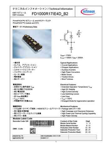
fd1000r17ie4.pdf
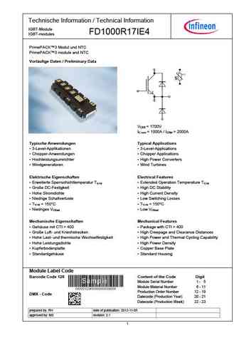
Technische Information / Technical Information IGBT-Module FD1000R17IE4 IGBT-modules PrimePACK 3 Modul und NTC PrimePACK 3 module and NTC Vorl ufige Daten / Preliminary Data V = 1700V CES I = 1000A / I = 2000A C nom CRM Typische Anwendungen Typical Applications 3-Level-Applikationen 3-Level-Applications Chopper-Anwendungen Chopper Applications Hochleistung
fd1000r33he3-k.pdf
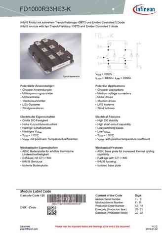
FD1000R33HE3-K IHM-B Modul mit schnellem Trench/Feldstopp IGBT3 und Emitter Controlled 3 Diode IHM-B module with fast Trench/Fieldstop IGBT3 and Emitter Controlled 3 diode V = 3300V CES I = 1000A / I = 2000A C nom CRM Potentielle Anwendungen Potential Applications Chopper-Anwendungen Chopper applications Mittelspannungsantriebe Medium voltage converters Motorantrie
fd1000r33hl3-k.pdf
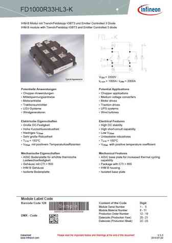
FD1000R33HL3-K IHM-B Modul mit Trench/Feldstopp IGBT3 und Emitter Controlled 3 Diode IHM-B module with Trench/Fieldstop IGBT3 and Emitter Controlled 3 diode V = 3300V CES I = 1000A / I = 2000A C nom CRM Potentielle Anwendungen Potential Applications Chopper-Anwendungen Chopper applications Mittelspannungsantriebe Medium voltage converters Motorantriebe Motor dr
ipd100n06s4-03.pdf
IPD100N06S4-03 OptiMOS -T2 Power-Transistor Product Summary V 60 V DS R 3.5 m DS(on),max I 100 A D Features PG-TO252-3-11 N-channel - Enhancement mode AEC Q101 qualified MSL1 up to 260 C peak reflow 175 C operating temperature Green Product (RoHS compliant) 100% Avalanche tested Ultra Low RDSon Ultra High ID Type Package Marking IPD100N
mid100-12a3.pdf
MID100-12A3 VCES = 1200V IGBT (NPT) Module I= 135A C25 VCE(sat) = 2.2V Boost Chopper + free wheeling Diode Part number MID100-12A3 Backside isolated 1 3 4 5 2 Features / Advantages Applications Package Y4 NPT IGBT technology AC motor drives Isolation Voltage V 3600 low saturation voltage Solar inverter Industry standard outline low switching
d1002uk.pdf
TetraFET D1002UK ROHS COMPLIANT METAL GATE RF SILICON FET MECHANICAL DATA GOLD METALLISED A MULTI-PURPOSE SILICON B C DMOS RF FET 1 2 40W 28V 175MHz D 4 3 E SINGLE ENDED M F G FEATURES SIMPLIFIED AMPLIFIER DESIGN H K I J SUITABLE FOR BROAD BAND APPLICATIONS DA LOW Crss PIN 1 SOURCE PIN 2 DRAIN PIN 3 SOURCE PIN 4 GATE SIMPLE BIAS CIRCUITS
d1001uk.pdf

TetraFET D1001UK ROHS COMPLIANT METAL GATE RF SILICON FET MECHANICAL DATA GOLD METALLISED A MULTI-PURPOSE SILICON B C DMOS RF FET 1 2 20W 28V 175MHz D 4 3 E SINGLE ENDED M F G FEATURES SIMPLIFIED AMPLIFIER DESIGN H K I J SUITABLE FOR BROAD BAND APPLICATIONS DA LOW Crss PIN 1 SOURCE PIN 2 DRAIN PIN 3 SOURCE PIN 4 GATE SIMPLE BIAS CIRCUITS
pmd18d100.pdf
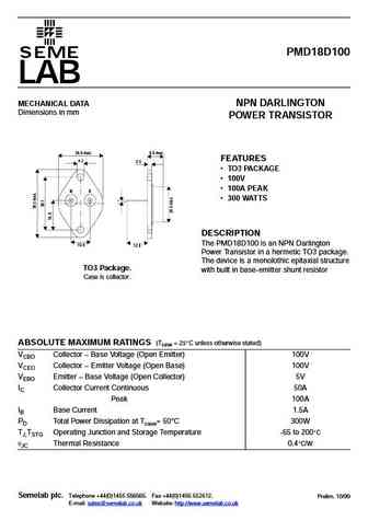
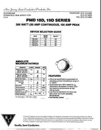
PMD18D100 SEME LAB MECHANICAL DATA NPN DARLINGTON Dimensions in mm POWER TRANSISTOR 26.6 max. 9.0 max. FEATURES 4. 2 2. 5 TO3 PACKAGE 100V 100A PEAK B E 300 WATTS DESCRIPTION The PMD18D100 is an NPN Darlington 10.9 12.8 Power Transistor in a hermetic TO3 package. The device is a monolothic epitaxial structure TO3 Package. with built in base-emitter shunt r
d1007uk.pdf
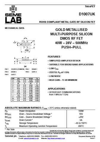
TetraFET D1007UK ROHS COMPLIANT METAL GATE RF SILICON FET MECHANICAL DATA GOLD METALLISED MULTI-PURPOSE SILICON A DMOS RF FET B C K 2 3 (2 pls) 1 40W 28V 500MHz E D 5 4 PUSH PULL G (4 pls) F O FEATURES SIMPLIFIED AMPLIFIER DESIGN H J I M N SUITABLE FOR BROAD BAND APPLICATIONS DK LOW Crss PIN 1 SOURCE (COMMON) PIN 2 DRAIN 1 PIN 3 DRAIN 2 PIN 4 GA
2sd1005.pdf
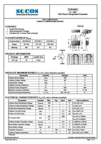
2SD1005 1A , 100V NPN Plastic Encapsulated Transistor Elektronische Bauelemente RoHS Compliant Product A suffix of -C specifies halogen & lead-free SOT-89 FEATURES Small Flat Package 4 High Breakdown Voltage Excellent DC Current Gain Linearity 1 2 3 B C A E E C CLASSIFICATION OF hFE(1) Product-Rank 2SD1005-W 2SD1005-V 2SD1005-U B D Range 90 180 1
2sd1005.pdf
JIANGSU CHANGJIANG ELECTRONICS TECHNOLOGY CO., LTD SOT-89-3L Plastic-Encapsulate Transistors SOT-89-3L 2SD1005 TRANSISTOR (NPN) 1. BASE FEATURES 2. COLLECTOR Small Flat Package High Breakdown Voltage 3. EMITTER Excellent DC Current Gain Linearity MAXIMUM RATINGS (Ta=25 unless otherwise noted) Symbol Parameter Value Unit VCBO Collector-Base Voltage 100 V VCEO C
ktd1003.pdf
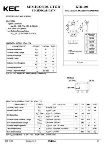
SEMICONDUCTOR KTD1003 TECHNICAL DATA EPITAXIAL PLANAR NPN TRANSISTOR HIGH CURRENT APPLICATION. A C FEATURES G H High DC Current Gain L M hFE=800 3200. (VCE=5.0V, IC=300mA). Wide Area of Safe Operation. N Low Collector Saturation Voltage D D VCE(sat)=0.17V (IC=500mA, IB=5.0mA). K DIM MILLIMETERS F F A 4.70 MAX _ + B 2.50 0.20 C 1.70 MAX D 0.45+0.15/-0.10 1
2sd1005.pdf
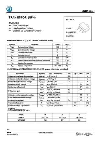
2SD1005 TRANSISTOR (NPN) SOT-89-3L FEATURES Small Flat Package 1. BASE High Breakdown Voltage Excellent DC Current Gain Linearity 2. COLLECTOR 3. EMITTER MAXIMUM RATINGS (Ta=25 unless otherwise noted) Symbol Parameter Value Unit VCBO Collector-Base Voltage 100 V VCEO Collector-Emitter Voltage 80 V VEBO Emitter-Base Voltage 5 V IC Collector Current 1 A PC Coll
brd100n03.pdf
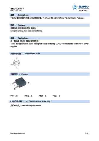
BRD100N03 Rev.A .Jun. -2017 DATA SHEET / Descriptions TO-252 N MOS N-CHANNEL MOSFET in a TO-252 Plastic Package. / Features , , Low gate charge, low crss, fast switching. / Applications DC/DC These devices are well suited for high effici
3cd100.pdf
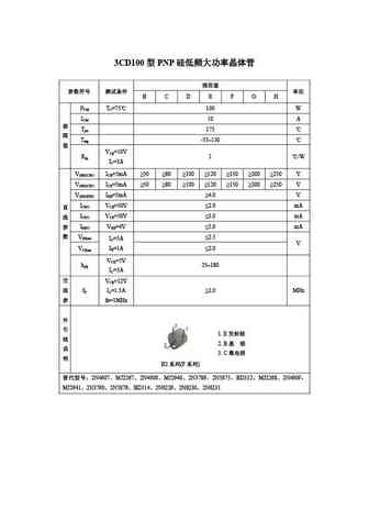
3CD100 PNP B C D E F G H PCM TC=75 100 W ICM 10 A Tjm 175 Tstg -55 150 VCE=10V Rth 1 /W IC=3A V(BR)CBO ICB=5mA 50 80 100 120 150 200 250 V V(BR)CEO ICE=5mA 50 80 100 120 150 200 250 V V(BR)EBO IEB=5mA 4.0 V ICBO VCB=50V
dh100n03b13 dhf100n03b13 dhi100n03b13 dhe100n03b13 dhb100n03b13 dhd100n03b13.pdf
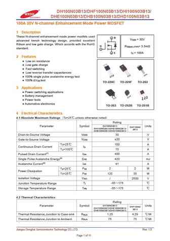
DH100N03B13/DHF100N03B13/DHI100N03B13/ DHE100N03B13/DHB100N03B13/DHD100N03B13 100A 30V N-channel Enhancement Mode Power MOSFET 1 Description These N-channel enhancement mode power mosfets used 2 D V = 30V DSS advanced trench technology design, provided excellent Rdson and low gate charge. Which accords with the RoHS G R = 3.3m DS(on) (TYP) standard. 1 3 S I = 100A D 2 Featur
ntd100n02.pdf
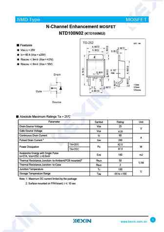
SMD Type MOSFET N-Channel Enhancement MOSFET NTD100N02 (KTD100N02) TO-252 U t m ni m Features 6. 50+0. 15 - 0. 15 +0. 1 2. 30 - 0. 1 +0. 2 VDS (V) = 25V 5. 30- 0. 2 +0. 8 0. 50 - 0. 7 ID = 60 A (VGS = 20V) 4 RDS(ON) 9m (VGS = 4.5V) RDS(ON) 6m (VGS = 10V) 0. 127 0. 80+0. 1 m - 0. 1 ax Drain 1 Gate + 0. 1 2 Drain 2. 3 0. 60- 0. 1
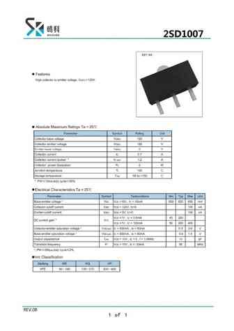
2sd1007.pdf
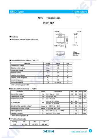
SMD Type Transistors NPN Transistors 2SD1007 1.70 0.1 Features High collector to emitter voltage VCEO 120V. 0.42 0.1 0.46 0.1 1.Base 2.Collector 3.Emitter Absolute Maximum Ratings Ta = 25 Parameter Symbol Rating Unit Collector-base voltage VCBO 120 V Collector-emitter voltage VCEO 120 V Emitter-base voltage VEBO 5 V Collector current IC 0.7 A Collector current (pulse) * IC (pu
2sd1005.pdf
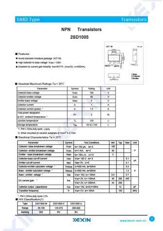
SMD Type Transistors NPN Tr ansistors 2SD1005 1.70 0.1 Features World standard miniature package SOT-89. High collector to base voltage VCBO 100V. 0.42 0.1 0.46 0.1 Excellent dc current gain linearity hFE=80TYP. (VCE=2V, IC=500mA). 1.Base 2.Collector 3.Emitter Absolute Maximum Ratings Ta = 25 Parameter Symbol Rating Unit Collector-base voltage VCBO 100 V Collector-emitter vo
2sd1006.pdf
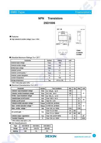
SMD Type Transistors SMD Type NPN Transistors 2SD1006 1.70 0.1 Features High collector to emitter voltage VCEO 100V. 0.42 0.1 0.46 0.1 1.Base 2.Collector 3.Emitter Absolute Maximum Ratings Ta = 25 Parameter Symbol Rating Unit Collector-base voltage VCBO 100 V Collector-emitter voltage VCEO 100 V Emitter-base voltage VEBO 5 V Collector current IC 0.7 A Collector current (pulse
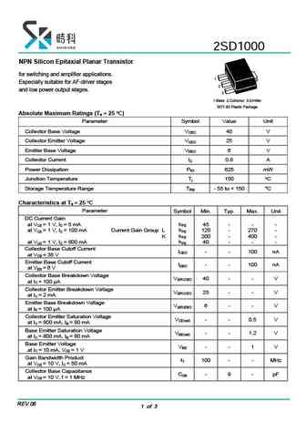
2sd1000.pdf
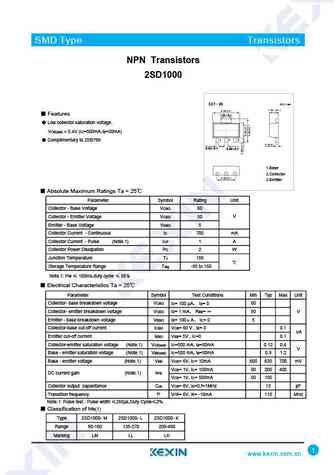
SMD Type Transistors NPN Transistors 2SD1000 Features 1.70 0.1 Low collector saturation voltage. VCE(sat)
2sd1001.pdf
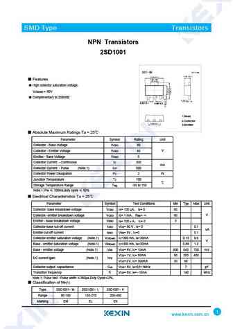
SMD Type Transistors NPN Transistors 2SD1001 Features 1.70 0.1 High collector saturation voltage. VCE(sat) > 80V Complimentary to 2SB800 0.42 0.1 0.46 0.1 1.Base 2.Collector 3.Emitter Absolute Maximum Ratings Ta = 25 Parameter Symbol Rating Unit Collector - Base Voltage VCBO 80 Collector - Emitter Voltage VCEO 80 V Emitter - Base Voltage VEBO 5 Collect
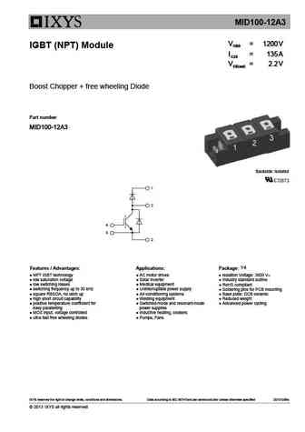
mpmd100b120rh.pdf

MPMD100B120RH NPT & Rugged Type 1200V IGBT Module General Description Features MagnaChip s IGBT Module 7DM-3 package BVCES= 1200V Low Conduction Loss VCE(sat) = 2.7V (typ.) devices are optimized to reduce losses and Fast & Soft Anti-Parallel FWD switching noise in high frequency power Short circuit rated Min. 10us at TC=100 Isolation Type Packa
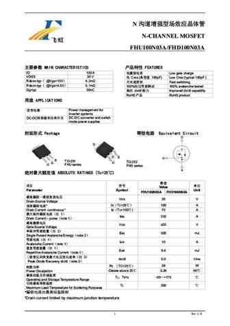
fhu100n03c fhd100n03c fhp100n03c.pdf

N N-CHANNEL MOSFET FHU100N03C/FHD100N03C/FHP100N03C MAIN CHARACTERISTICS FEATURES ID 100 A Low gate charge VDSS 30 V Crss ( 261pF) Low Crss (typical 261pF ) Rdson-typ @Vgs=10V 3.7m Fast switching Rdson-typ @Vgs=4.5V 5.1m 100% 100% avala
fhu100n03b fhd100n03b fhp100n03b.pdf
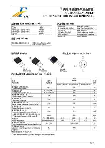
N N-CHANNEL MOSFET FHU100N03B/FHD100N03B/FHP100N03B MAIN CHARACTERISTICS FEATURES ID 100 A Low gate charge VDSS 30 V Crss ( 261pF) Low Crss (typical 261pF ) Rdson-typ @Vgs=10V 4.9m Fast switching Rdson-typ @Vgs=4.5V 7.2m 100% 100% avala
fhd100.pdf
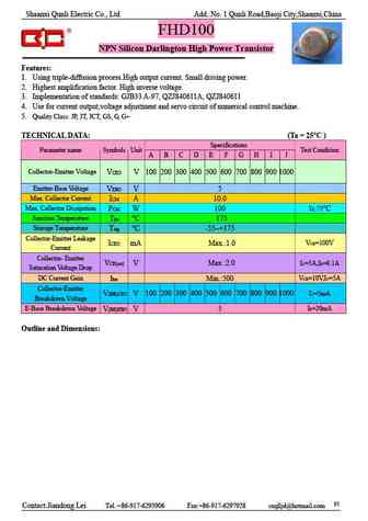
Shaanxi Qunli Electric Co., Ltd Add. No. 1 Qunli Road,Baoji City,Shaanxi,China FHD100 NPN Silicon Darlington High Power Transistor Features 1. Using triple-diffusion process.High output current. Small driving power. 2. Highest amplification factor. High inverse voltage. 3. Implementation of standards GJB33 A-97, QZJ840611A, QZJ840611 4. Use for current output,voltage adjustment a
2sd1000l 2sd1000k.pdf
2SD1000 NPN Silicon Epitaxial Planar Transistor for switching and amplifier applications. Especially suitable for AF-driver stages and low power output stages. O Absolute Maximum Ratings (Ta = 25 C) Parameter Symbol Value Unit Collector Base Voltage VCBO 40 V Collector Emitter Voltage VCEO 25 V Emitter Base Voltage VEBO 6 V Collector Current IC 0.8 A Power Dissipation Ptot 625
2sd1005bw 2sd1005bv 2sd1005bu.pdf
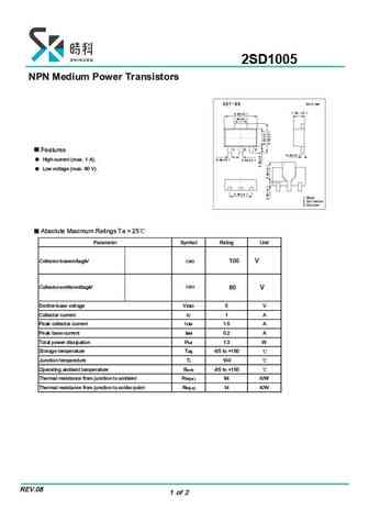
2SD1005 NPN Medium Power Transistors Features High current (max. 1 A). Low voltage (max. 80 V). Absolute Maximum Ratings Ta = 25 Parameter Symbol Rating Unit Collector-basevoltage CBO 100 V V CEO Collector-emittervoltageV 80 V Emitter-base voltage VEBO 5V Collector current IC 1A Peak collector current ICM 1.5 A Peak base current IBM 0.2 A Total power dissipation Ptot 1.3 W Stor
hgd100n12sl.pdf
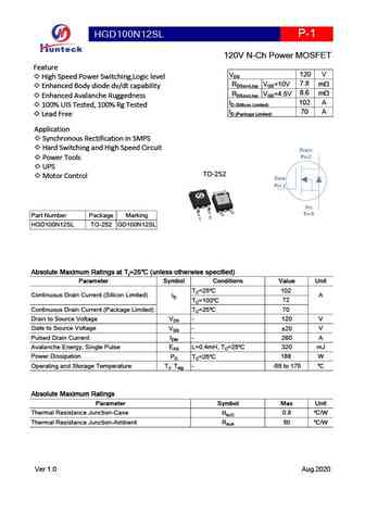
HGD100N12SL P-1 120V N-Ch Power MOSFET Feature 120 V VDS High Speed Power Switching,Logic level 7.8 RDS(on),typ VGS=10V mW Enhanced Body diode dv/dt capability 8.6 RDS(on),typ VGS=4.5V mW Enhanced Avalanche Ruggedness 102 A ID (Sillicon Limited) 100% UIS Tested, 100% Rg Tested 70 A ID (Package Limited) Lead Free Application Synchronous Rectification in
hgd100n12s.pdf
HGD100N12S P-1 120V N-Ch Power MOSFET Feature 120 V VDS High Speed Power Switching TO-252 8.6 RDS(on),typ m Enhanced Body diode dv/dt capability 102 A ID (Sillicon Limited) Enhanced Avalanche Ruggedness 70 A ID (Package Limited) 100% UIS Tested, 100% Rg Tested Lead Free Application Synchronous Rectification in SMPS Hard Switching and High Speed C
wsd100n06gdn56.pdf
WSD100N06GDN56 N-Ch MOSFET General Description Product Summery BVDSS RDSON ID The WSD100N06GDN56 is the SGT MOSFET with extreme high cell density,which provide 60V 100A 3.0m excellent RDSON and gate charge for most of the synchronous buck converter applications . Applications Secondary Side Synchronous Rectification The WSD100N06GDN56 meet the RoHS and Green Product requi
sed10070gg.pdf

SED10070GG N-Channel Enhancement-Mode MOSFET Revision A General Description Features For a single MOSFET Advanced trench technology to provide excellent RDS(ON), low gate charge and low V =100V DS operation voltage. This device is suitable for R =8.2m @V =10V DS(ON) GS using as a load switch or in PWM applications. Simple Drive Requirement Small Package Outline
sed10080gg.pdf
SED10080GG N-Channel Enhancement-Mode MOSFET Revision A General Description Features For a single MOSFET Advanced trench technology to provide excellent RDS(ON), low gate charge and low V =100V DS operation voltage. This device is suitable for R =6.7m @V =10V DS(ON) GS using as a load switch or in PWM applications. Simple Drive Requirement Small Package Outline
ttd100n04at ttp100n04at.pdf
TTD100N04AT, TTP100N04AT Wuxi Unigroup Microelectronics Company Wuxi Unigroup Microelectronics Company 40V N-Channel Trench MOSFET FEATURES Trench Power MOSFET Technology Low RDS(ON) Low Gate Charge Optimized For Fast-switching Applications APPLICATIONS Synchronous Rectification in DC/DC and AC/DC Converters Isolated DC/DC Converters in Telecom and
2sd1007.pdf
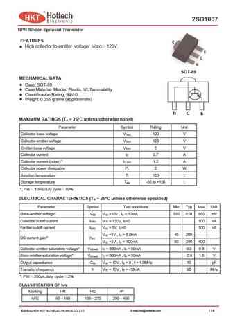
2SD1007 NPN Silicon Epitaxial Transistor FEATURES High collector to emitter voltage VCEO 120V. SOT-89 MECHANICAL DATA Case SOT-89 Case Material Molded Plastic. UL flammability Classification Rating 94V-0 Weight 0.055 grams (approximate) MAXIMUM RATINGS (T = 25 C unless otherwise noted) A Parameter Symbol Rating Unit Collector-base voltage V 120 V CBO Co
md100n20.pdf
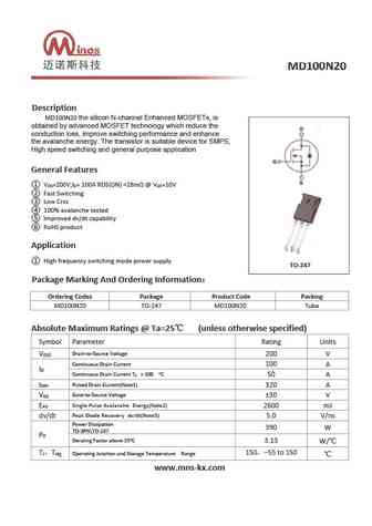
Description MD100N20 the silicon N-channel Enhanced MOSFETs, is obtained by advanced MOSFET technology which reduce the conduction loss, improve switching performance and enhance the avalanche energy. The transistor is suitable device for SMPS, High speed switching and general purpose application General Features V =200V,I = 100A RDS(ON)
gd100hfx65c1s.pdf
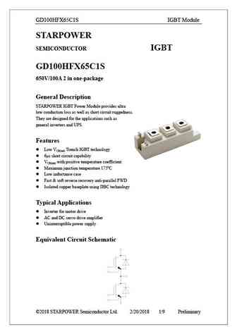
GD100HFX65C1S IGBT Module STARPOWER SEMICONDUCTOR IGBT GD100HFX65C1S 650V/100A 2 in one-package General Description STARPOWER IGBT Power Module provides ultra low conduction loss as well as short circuit ruggedness. They are designed for the applications such as general inverters and UPS. Features Low VCE(sat) Trench IGBT technology 6 s short circuit capability
std100n10f7.pdf
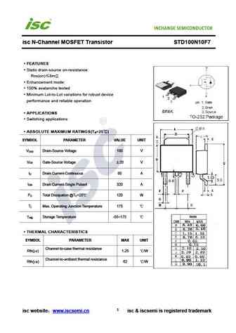
isc N-Channel MOSFET Transistor STD100N10F7 FEATURES Static drain-source on-resistance RDS(on) 8m Enhancement mode 100% avalanche tested Minimum Lot-to-Lot variations for robust device performance and reliable operation APPLICATIONS Switching applications ABSOLUTE MAXIMUM RATINGS(T =25 ) a SYMBOL PARAMETER VALUE UNIT V Drain-Source Voltage 100 V DSS V Gat
ipd100n04s4-02.pdf
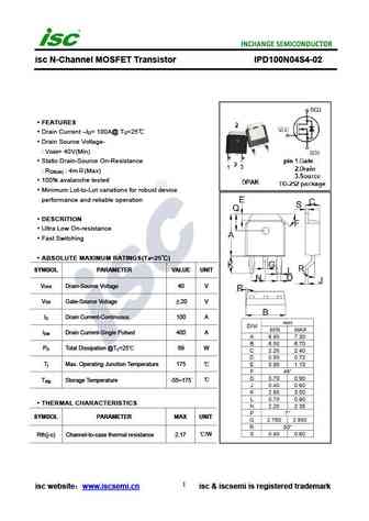
isc N-Channel MOSFET Transistor IPD100N04S4-02 FEATURES Drain Current I = 100A@ T =25 D C Drain Source Voltage- V = 40V(Min) DSS Static Drain-Source On-Resistance R 4m (Max) DS(on) 100% avalanche tested Minimum Lot-to-Lot variations for robust device performance and reliable operation DESCRITION Ultra Low On-resistance Fast Switching ABSOLUTE MAX
3dd100e.pdf
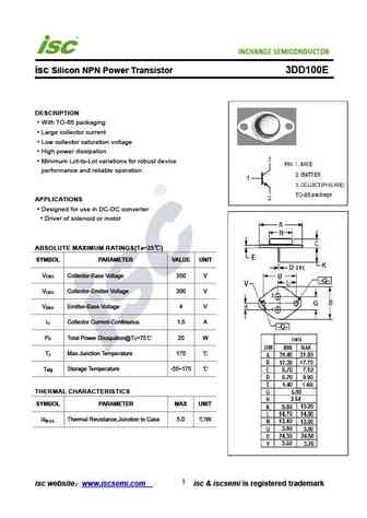
INCHANGE Semiconductor isc Product Specification isc Silicon NPN Power Transistor 3DD100E DESCRIPTION With TO-66 packaging Large collector current Low collector saturation voltage High power dissipation Minimum Lot-to-Lot variations for robust device performance and reliable operation APPLICATIONS Designed for use in DC-DC converter Driver of solenoid or motor ABSOLUTE
3dd100c.pdf
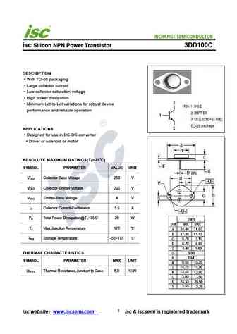
E Semiconductor isc Product Specification isc Silicon NPN Power Transistor 3DD100C DESCRIPTION With TO-66 packaging Large collector current Low collector saturation voltage High power dissipation Minimum Lot-to-Lot variations for robust device performance and reliable operation APPLICATIONS Designed for use in DC-DC converter Driver of solenoid or motor ABSOLUTE MAXIMU
3dd100b.pdf
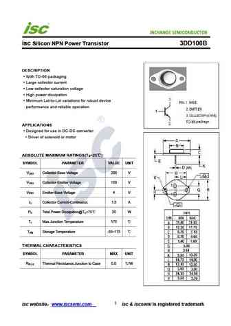
INCHANGE Semiconductor isc Silicon NPN Power Transistor 3DD100B DESCRIPTION With TO-66 packaging Large collector current Low collector saturation voltage High power dissipation Minimum Lot-to-Lot variations for robust device performance and reliable operation APPLICATIONS Designed for use in DC-DC converter Driver of solenoid or motor ABSOLUTE MAXIMUM RATINGS(T =25 )
3dd100d.pdf
INCHANGE Semiconductor isc Product Specification isc Silicon NPN Power Transistor 3DD100D DESCRIPTION With TO-66 packaging Large collector current Low collector saturation voltage High power dissipation Minimum Lot-to-Lot variations for robust device performance and reliable operation APPLICATIONS Designed for use in DC-DC converter Driver of solenoid or motor ABSOLUTE
3dd100a.pdf
isc Silicon NPN Power Transistor 3DD100A DESCRIPTION With TO-66 packaging Large collector current Low collector saturation voltage High power dissipation Minimum Lot-to-Lot variations for robust device performance and reliable operation APPLICATIONS Designed for use in DC-DC converter Driver of solenoid or motor ABSOLUTE MAXIMUM RATINGS(T =25 ) a SYMBOL PARAMETER VA
Другие транзисторы: CZT5401, CZT5551, CZTA14, CZTA27, CZTA42, CZTA44, CZTA64, CZTA92, B647, D100P, D10-28B, D10B1051, D10B1055, D10G1051, D10G1052, D115, D11B1052
🌐 : EN ES РУ

Список транзисторов
Обновления
BJT: GA1A4M | SBT42 | 2SA200-Y | 2SA200-O | 2SD882-Q | 2SD882-P | 2SD882-E | 2SC945-L | 2SC945-H | 2SC4226-R23 | 2SC3357-F | 2SC3357-E | 2SC3356-R26 | 2SC3356-R24 | 2SC3356-R23 | 2SB772-Q | 2SB772-P | 2SB772-E | 2SA1015-L | 2SA1015-H | HSS8550
Popular searches
2sc458 replacement | bc557 transistor | 2n3638 | tip127 datasheet | irlz24n | irf620 | irfp350 | 13003 transistor