T11 datasheet, аналоги, основные параметры
Наименование производителя: T11 📄📄
Маркировка: T11
Тип материала: Si
Полярность: NPN
Предельные значения
Максимальная рассеиваемая мощность (Pc): 0.25 W
Макcимально допустимое напряжение коллектор-база (Ucb): 50 V
Макcимально допустимое напряжение коллектор-эмиттер (Uce): 45 V
Макcимально допустимое напряжение эмиттер-база (Ueb): 5 V
Макcимальный постоянный ток коллектора (Ic): 0.1 A
Предельная температура PN-перехода (Tj): 150 °C
Электрические характеристики
Граничная частота коэффициента передачи тока (ft): 150 MHz
Ёмкость коллекторного перехода (Cc): 3.5 pf
Статический коэффициент передачи тока (hFE): 200
Корпус транзистора: SOT143
📄📄 Копировать
Аналоги (замена) для T11
- подборⓘ биполярного транзистора по параметрам
T11 даташит
t11.pdf
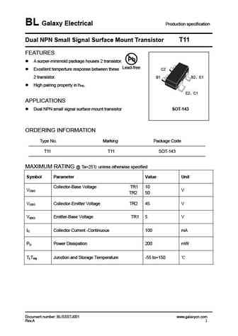
BL Galaxy Electrical Production specification Dual NPN Small Signal Surface Mount Transistor T11 FEATURES Pb A surper-minimold package houses 2 transistor. Excellent temperture response between these Lead-free C2 2 transistor. B1 B2 E1 High pairing property in hFE. E2 C1 APPLICATIONS Dual NPN small signal surface mount transistor SOT-143 ORDERING INFORMATION
apt11gf120brd.pdf
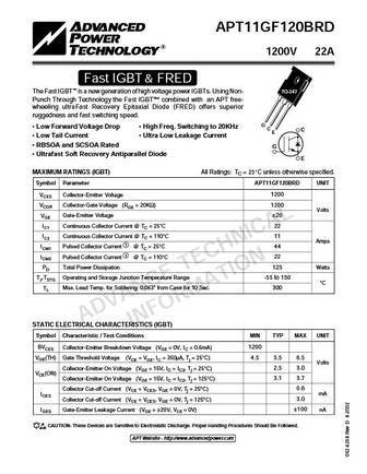
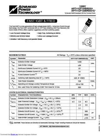
APT11GF120BRD 1200V 22A Fast IGBT & FRED The Fast IGBT is a new generation of high voltage power IGBTs. Using Non- TO-247 Punch Through Technology the Fast IGBT combined with an APT free- wheeling ultraFast Recovery Epitaxial Diode (FRED) offers superior ruggedness and fast switching speed. G Low Forward Voltage Drop High Freq. Switching to 20KHz C C E Low Tail Cur
gt110n06d5.pdf
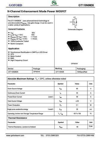
GOFORD GT110N06D5 N-Channel Enhancement Mode Power MOSFET Description The GT110N06D5 uses advanced trench technology to provide excellent RDS(ON) , low gate charge. It can be used in a wide variety of applications. General Features Schematic Diagram VDS 60V ID (at VGS = 10V) 45A RDS(ON) (at VGS = 10V)
but11afr.pdf
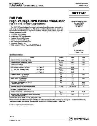
Order this document MOTOROLA by BUT11AF/D SEMICONDUCTOR TECHNICAL DATA BUT11AF Full Pak High Voltage NPN Power Transistor POWER TRANSISTOR 5.0 AMPERES For Isolated Package Applications 450 VOLTS 40 WATTS The BUT11AF was designed for use in line operated switching power supplies in a wide range of end use applications. This device combines the latest state of the art bipolar fabric
but11apx.pdf
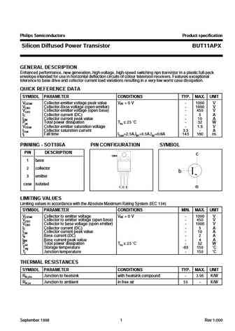
Philips Semiconductors Product specification Silicon Diffused Power Transistor BUT11APX GENERAL DESCRIPTION Enhanced performance, new generation, high-voltage, high-speed switching npn transistor in a plastic full-pack envelope intended for use in horizontal deflection circuits of colour television receivers. Features exceptional tolerance to base drive and collector current load variati
but11ai.pdf

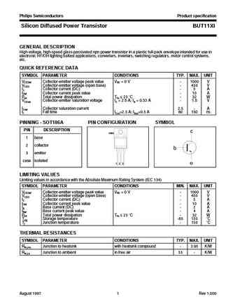
Philips Semiconductors Product specification Silicon Diffused Power Transistor BUT11AI GENERAL DESCRIPTION Enhanced performance, high speed switching npn transistor in TO220AB envelope specially suited for high frequency electronic lighting ballast applications and converters, inverters, switching regulators, motor control systems etc. QUICK REFERENCE DATA SYMBOL PARAMETER CONDITIONS T
but11f 1.pdf
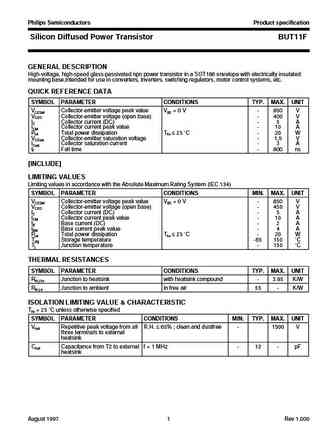
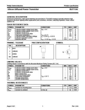
Philips Semiconductors Product specification Silicon Diffused Power Transistor BUT11F GENERAL DESCRIPTION High-voltage, high-speed glass-passivated npn power transistor in a SOT186 envelope with electrically insulated mounting base,intended for use in converters, inverters, switching regulators, motor control systems, etc. QUICK REFERENCE DATA SYMBOL PARAMETER CONDITIONS TYP. MAX. UNIT
pht11n06t 1.pdf
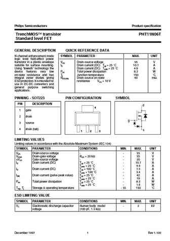
Philips Semiconductors Product specification TrenchMOS transistor PHT11N06T Standard level FET GENERAL DESCRIPTION QUICK REFERENCE DATA N-channel enhancement mode SYMBOL PARAMETER MAX. UNIT logic level field-effect power transistor in a plastic envelope VDS Drain-source voltage 55 V suitable for surface mounting. ID Drain current (DC) Tsp = 25 C 10.7 A Using trench technolo
but11xi 1.pdf
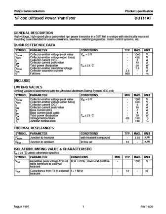
Philips Semiconductors Product specification Silicon Diffused Power Transistor BUT11XI GENERAL DESCRIPTION High-voltage, high-speed glass-passivated npn power transistor in a plastic full-pack envelope intended for use in electronic HF/OH lighting ballast applications, converters, inverters, switching regulators, motor control systems, etc. QUICK REFERENCE DATA SYMBOL PARAMETER CONDITI
but11ai 1.pdf
Philips Semiconductors Product specification Silicon Diffused Power Transistor BUT11AI GENERAL DESCRIPTION Enhanced performance, high speed switching npn transistor in TO220AB envelope specially suited for high frequency electronic lighting ballast applications and converters, inverters, switching regulators, motor control systems etc. QUICK REFERENCE DATA SYMBOL PARAMETER CONDITIONS T
but11ax 1.pdf

Philips Semiconductors Product specification Silicon Diffused Power Transistor BUT11AX GENERAL DESCRIPTION High-voltage, high-speed glass-passivated npn power transistor in a plastic full-pack envelope intended for use in converters, inverters, switching regulators, motor control systems, etc. QUICK REFERENCE DATA SYMBOL PARAMETER CONDITIONS TYP. MAX. UNIT VCESM Collector-emitter volta
but11ax.pdf
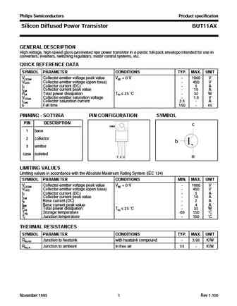
Philips Semiconductors Product specification Silicon Diffused Power Transistor BUT11AX GENERAL DESCRIPTION High-voltage, high-speed glass-passivated npn power transistor in a plastic full-pack envelope intended for use in converters, inverters, switching regulators, motor control systems, etc. QUICK REFERENCE DATA SYMBOL PARAMETER CONDITIONS TYP. MAX. UNIT VCESM Collector-emitter volta
but11af 1.pdf
Philips Semiconductors Product specification Silicon Diffused Power Transistor BUT11AF GENERAL DESCRIPTION High-voltage, high-speed glass-passivated npn power transistor in a SOT186 envelope with electrically insulated mounting base,intended for use in converters, inverters, switching regulators, motor control systems, etc. QUICK REFERENCE DATA SYMBOL PARAMETER CONDITIONS TYP. MAX. UNIT
pht11n06lt 2.pdf
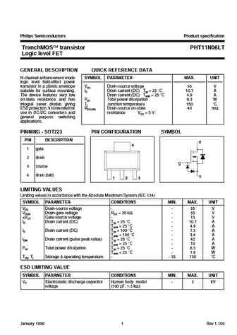
Philips Semiconductors Product specification TrenchMOS transistor PHT11N06LT Logic level FET GENERAL DESCRIPTION QUICK REFERENCE DATA N-channel enhancement mode SYMBOL PARAMETER MAX. UNIT logic level field-effect power transistor in a plastic envelope VDS Drain-source voltage 55 V suitable for surface mounting. ID Drain current (DC) Tsp = 25 C 10.7 A The device features very low
but11 1.pdf
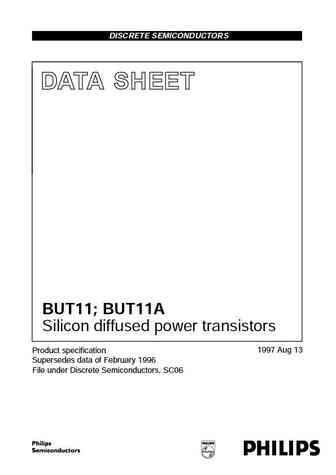
DISCRETE SEMICONDUCTORS DATA SHEET BUT11; BUT11A Silicon diffused power transistors 1997 Aug 13 Product specification Supersedes data of February 1996 File under Discrete Semiconductors, SC06 Philips Semiconductors Product specification Silicon diffused power transistors BUT11; BUT11A DESCRIPTION High-voltage, high-speed, glass-passivated NPN power transistor in a TO-220AB package
but110.pdf
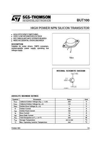
BUT100 HIGH POWER NPN SILICON TRANSISTOR n HIGH EFFICIENCY SWITCHING n VERY LOW SATURATION VOLTAGE n RECTANGULAR SAFE OPERATION AREA n WIDE ACCIDENTAL OVERLOAD AREA DESCRIPTION Suitable for motor drivers, SMPS converters, uninterruptable power supply operating low 1 voltage supply. 2 TO-3 INTERNAL SCHEMATIC DIAGRAM ABSOLUTE MAXIMUM RATINGS Symbol Parameter Value Unit VCEV Collec
bult118d.pdf
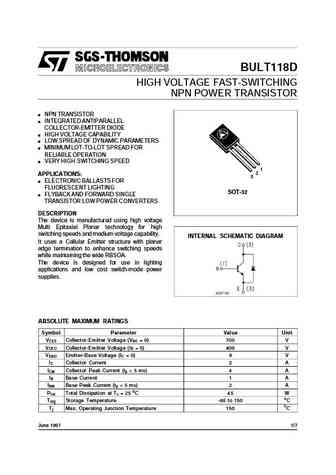
BULT118D HIGH VOLTAGE FAST-SWITCHING NPN POWER TRANSISTOR NPN TRANSISTOR INTEGRATED ANTIPARALLEL COLLECTOR-EMITTER DIODE HIGH VOLTAGE CAPABILITY LOW SPREAD OF DYNAMIC PARAMETERS MINIMUM LOT-TO-LOT SPREAD FOR RELIABLE OPERATION VERY HIGH SWITCHING SPEED 1 2 APPLICATIONS 3 ELECTRONIC BALLASTS FOR FLUORESCENT LIGHTING SOT-32 FLYBACK AND FORWARD SINGLE TRANSISTOR LOW POW
but11a.pdf
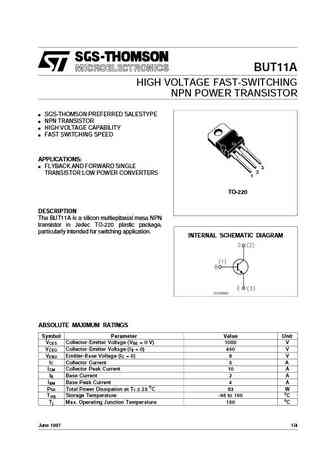
BUT11A HIGH VOLTAGE FAST-SWITCHING NPN POWER TRANSISTOR SGS-THOMSON PREFERRED SALESTYPE NPN TRANSISTOR HIGH VOLTAGE CAPABILITY FAST SWITCHING SPEED APPLICATIONS FLYBACK AND FORWARD SINGLE 3 2 TRANSISTOR LOW POWER CONVERTERS 1 TO-220 DESCRIPTION The BUT11A is a silicon multiepitaxial mesa NPN transistor in Jedec TO-220 plastic package, particularly intended for switch
bult116d.pdf

BULT116D MEDIUM VOLTAGE FAST-SWITCHING NPN POWER TRANSISTOR PRELIMINARY DATA INTEGRATED ANTIPARALLEL COLLECTOR- EMITTER DIODE LOW SPREAD OF DYNAMIC PARAMETERS MINIMUM LOT-TO-LOT SPREAD FOR RELIABLE OPERATION VERY HIGH SWITCHING SPEED APPLICATIONS COMPACT FLUORESCENT LAMPS UP TO 1 2 23 W AT 110 V A.C. MAINS 3 FLYBACK AND FORWARD SINGLE TRANSISTOR LOW POWER CONVERTERS
bult118.pdf
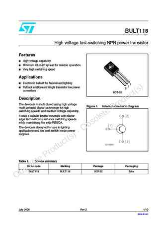
BULT118 High voltage fast-switching NPN power transistor Features High voltage capability Minimum lot-to-lot spread for reliable operation Very high switching speed Applications Electronic ballast for fluorescent lighting 1 2 Flyback and forward single transistor low power 3 converters SOT-32 Description The device is manufactured using high voltage Figure
rej03g0446 hat1111c.pdf

To our customers, Old Company Name in Catalogs and Other Documents On April 1st, 2010, NEC Electronics Corporation merged with Renesas Technology Corporation, and Renesas Electronics Corporation took over all the business of both companies. Therefore, although the old company name remains in this document, it is a valid Renesas Electronics document. We appreciate your understanding.
rej03g1234 hat1108c.pdf

To our customers, Old Company Name in Catalogs and Other Documents On April 1st, 2010, NEC Electronics Corporation merged with Renesas Technology Corporation, and Renesas Electronics Corporation took over all the business of both companies. Therefore, although the old company name remains in this document, it is a valid Renesas Electronics document. We appreciate your understanding.
rej03g1330 hat1127hds.pdf
To our customers, Old Company Name in Catalogs and Other Documents On April 1st, 2010, NEC Electronics Corporation merged with Renesas Technology Corporation, and Renesas Electronics Corporation took over all the business of both companies. Therefore, although the old company name remains in this document, it is a valid Renesas Electronics document. We appreciate your understanding.
rej03g1244 hat1139h.pdf

To our customers, Old Company Name in Catalogs and Other Documents On April 1st, 2010, NEC Electronics Corporation merged with Renesas Technology Corporation, and Renesas Electronics Corporation took over all the business of both companies. Therefore, although the old company name remains in this document, it is a valid Renesas Electronics document. We appreciate your understanding.
hat1128r.pdf
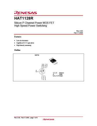
HAT1128R Silicon P Channel Power MOS FET High Speed Power Switching Rev.3.00 Feb.17.2004 Features Low on-resistance Capable of 4.5 V gate drive High density mounting Outline SOP-8 5 6 7 8 4 3 2 5 6 7 8 1 D D D D 4 G 1, 2, 3 Source 4 Gate 5, 6, 7, 8 Drain S S S 1 2 3 Rev.3.00, Feb.17.2005, page 1 of 8 HAT1128R Absolute Maximum Ratings (Ta =
rej03g0406 hat1126rrj.pdf

To our customers, Old Company Name in Catalogs and Other Documents On April 1st, 2010, NEC Electronics Corporation merged with Renesas Technology Corporation, and Renesas Electronics Corporation took over all the business of both companies. Therefore, although the old company name remains in this document, it is a valid Renesas Electronics document. We appreciate your understanding.
rej03g0416 hat1110r.pdf

To our customers, Old Company Name in Catalogs and Other Documents On April 1st, 2010, NEC Electronics Corporation merged with Renesas Technology Corporation, and Renesas Electronics Corporation took over all the business of both companies. Therefore, although the old company name remains in this document, it is a valid Renesas Electronics document. We appreciate your understanding.
but11a but11.pdf
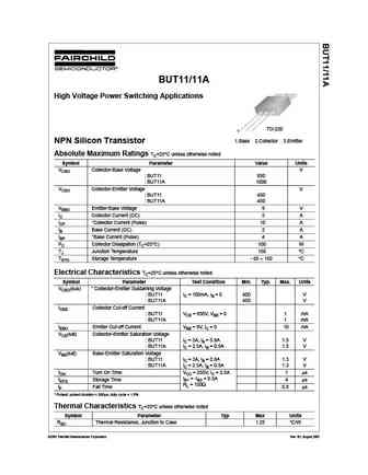
BUT11/11A High Voltage Power Switching Applications TO-220 1 1.Base 2.Collector 3.Emitter NPN Silicon Transistor Absolute Maximum Ratings TC=25 C unless otherwise noted Symbol Parameter Value Units VCBO Collector-Base Voltage V BUT11 850 BUT11A 1000 VCEO Collector-Emitter Voltage V BUT11 400 BUT11A 450 VEBO Emitter-Base Voltage 9 V IC Collector Current (DC) 5 A ICP
but11af but11f.pdf
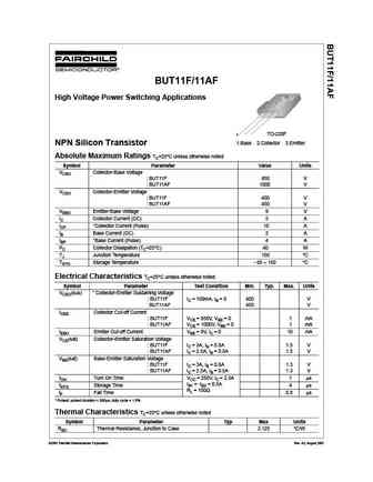
BUT11F/11AF High Voltage Power Switching Applications TO-220F 1 1.Base 2.Collector 3.Emitter NPN Silicon Transistor Absolute Maximum Ratings TC=25 C unless otherwise noted Symbol Parameter Value Units VCBO Collector-Base Voltage BUT11F 850 V BUT11AF 1000 V VCEO Collector-Emitter Voltage BUT11F 400 V BUT11AF 450 V VEBO Emitter-Base Voltage 9 V IC Collector Current (DC
but11.pdf
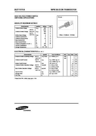
BUT11/11A NPN SILICON TRANSISTOR HIGH VOLTAGE POWER SWITCH TO-220 SWITCHING APPLICATIONS ABSOLUTE MAXIMUM RATINGS Characteristic Symbol Rating Unit Collector Base Voltage VCES 850 V BUT11 1000 V BUT11A Collector Emitter Voltage VCEO 400 V BUT11 450 V BUT11A Emitter Base Voltage VEBO 9 V 1.Base 2.Collector 3.Emitter Collector Current (DC) IC 5 A Collector Current (P
ruc002n05hzgt116.pdf
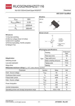
RUC002N05HZGT116 Datasheet Nch 50V 200mA Small Signal MOSFET AEC-Q101 Qualified lOutline l SOT-23 VDSS 50V SST3 RDS(on)(Max.) 2.2 ID 200mA PD 350mW lInner circuit l lFeatures l 1) Very fast switching 2) Ultra low voltage drive(1.2V drive) 3) AEC-Q101 Qualified 4) Pb-free lead plating ; RoHS compliant. 5) Halogen
vt6t11.pdf
Power management (dual transistors) VT6T11 Structure Dimensions (Unit mm) PNP silicon epitaxial planar transistor VMT6 0.5 0.1 1.2 0.1 (6) (5) (4) Features 0 0.05 1) Very small package with two transistors. (1) (2) (3) 2) Suitable for current mirror circuits. 0.16 0.05 0.13 0.05 0.4 0.4 0.8 0.1 Applications Current mirror circuits Abbreviated
rk7002bt116.pdf
2.5V Drive Nch MOSFET RK7002B Structure Dimensions (Unit mm) Silicon N-channel MOSFET SST3 Features 1) High speed switing. 2) Small package(SST3). 3) Low voltage drive(2.5V drive). Abbreviated symbol RKT Application Switching Packaging specifications Inner circuit (3) Package Taping Type Code T116 Basic ordering unit (pieces) 3000 RK7002B
mp6t11.pdf
Midium Power Transistors (-30V / -1A) MP6T11 Structure Dimensions (Unit mm) PNP Silicon epitaxial planar transistor MPT6 (Dual) Features (6) (5) (4) Low saturation voltage VCE (sat) = -0.35V (Max.) (IC / IB= -500mA / -25mA) (1) Tr.1 Emitter (1) (2) (3) (2) Tr.1 Base (3) Tr.2 Collector (4) Tr.2 Emitter Applications (5) Tr.2 Base (6) Tr.1 Collector Low Freque
rk7002t116.pdf
Transistors Interface and switching (60V, 115mA) RK7002 FFeatures FExternal dimensions (Units mm) 1) Low on-resistance. 2) Fast switching speed. 3) Low-voltage drive. 4) Easily designed drive circuits. 5) Easy to parallel. FStructure Silicon N-channel MOSFET FAbsolute maximum ratings (Ta = 25_C) FEquivalent circuit 186 Transistors RK7002 FElectrical characteristics (Ta = 25_C
rk7002at116.pdf
RK7002A Transistors Switching (60V, 300mA) RK7002A Features External dimensions (Units mm) 1) Low on-resistance. 2) High ESD 3) High-speed switching. 4) Low-voltage drive (4V). 5) Easily designed drive circuits. 1.3 6) Easy to use in parallel. 2.4 Structure Each lead has same dimensions Silicon N-channel MOSFET transistor ROHM SST3 (1) Source Abbreviated symbol RKS (2
j111 j112 j113 sst111 sst112 sst113.pdf
J/SST111 Series Vishay Siliconix N-Channel JFETs J111 SST111 J112 SST112 J113 SST113 PRODUCT SUMMARY Part Number VGS(off) (V) rDS(on) Max (W) ID(off) Typ (pA) tON Typ (ns) J/SST111 3 to 10 30 5 4 J/SST112 1 to 5 50 5 4 J/SST113 v 3 100 5 4 FEATURES BENEFITS APPLICATIONS D Low On-Resistance 111
zxt11n15df.pdf
ZXT11N15DF SuperSOT4 15V NPN SILICON LOW SATURATION TRANSISTOR SUMMARY VCEO=15V; RSAT = 37m ; IC= 3A DESCRIPTION This new 4th generation ultra low saturation transistor utilises the Zetex matrix structure combined with advanced assembly techniques to give SOT23 extremely low on state losses. This makes it ideal for high efficiency, low voltage switching applications. FEATURES
fzt1147a.pdf
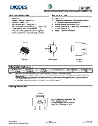
Green FZT1147A 12V PNP MEDIUM POWER HIGH GAIN TRANSISTOR IN SOT223 Features and Benefits Mechanical Data BVCEO > -12V Case SOT223 Maximum Continuous Current IC = -5A Case Material Molded Plastic, Green Molding Compound. UL Flammability Classification Rating 94V-0 Peak Pulse Current IC = -20A Moisture Sensitivity Level 1 per J-STD-020 High Gai
fzt1151a.pdf
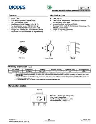
FZT1151A Green 40V PNP MEDIUM POWER TRANSISTOR IN SOT223 Features Mechanical Data BVCEO > -40V Case SOT223 IC = -3A High Continuous Collector Current Case Material Molded Plastic. Green Molding Compound; ICM = -5A Peak Pulse Current UL Flammability Rating 94V-0 Low Saturation Voltage VCE(sat)
fzt1149a.pdf
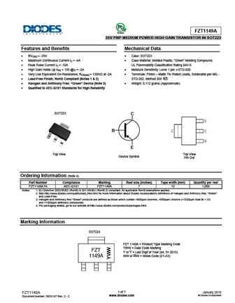
FZT1149A Green 25V PNP MEDIUM POWER HIGH GAIN TRANSISTOR IN SOT223 Features and Benefits Mechanical Data BVCEO > -25V Case SOT223 Maximum Continuous Current IC = -4A Case Material Molded Plastic, Green Molding Compound; Peak Pulse Current IC = -10A UL Flammability Classification Rating 94V-0 High Gain Holds Up hFE > 195 @IC = -2A Moisture Sensiti
ipt111n20nfd.pdf
IPT111N20NFD MOSFET HSOF OptiMOS 3 Power-Transistor, 200 V Features Tab N-channel, normal level Fast Diode (FD) with reduced Q rr Optimized for hard commutation ruggedness 1 Very low on-resistance R 2 DS(on) 3 4 5 175 C operating temperature 6 7 8 Pb-free lead plating; RoHS compliant Qualified according to JEDEC1) for target application H
ixth10p50 ixtt10p50 ixth11p50 ixtt11p50.pdf
VDSS ID25 RDS(on) Standard Power MOSFET P-Channel Enhancement Mode IXTH/IXTT 10P50 -500 V -10 A 0.90 Avalanche Rated IXTH/IXTT 11P50 -500 V -11 A 0.75 TO-247 AD (IXTH) Symbol Test Conditions Maximum Ratings VDSS TJ = 25 C to 150 C -500 V VDGR TJ = 25 C to 150 C; RGS = 1 M -500 V VGS Continuous 20 V (TAB) VGSM Transient 30 V D ID25 TC = 25 C 10P50 -10 A 11P50 -
ixth11p50 ixtt11p50.pdf
VDSS = -500 V Standard Power MOSFET ID25 = -11 A P-Channel Enhancement Mode IXTH 11P50 Avalanche Rated RDS(on) = 0.75 IXTT 11P50 TO-247 AD (IXTH) Symbol Test Conditions Maximum Ratings VDSS TJ = 25 C to 150 C -500 V VDGR TJ = 25 C to 150 C; RGS = 1 M -500 V VGS Continuous 20 V (TAB) VGSM Transient 30 V D ID25 TC = 25 C -11 A IDM TC = 25 C, p
ixtq110n10p ixtt110n10p.pdf
IXTQ 110N10P VDSS = 100 V PolarHTTM IXTT 110N10P ID25 = 110 A Power MOSFET RDS(on) 15 m N-Channel Enhancement Mode Avalanche Rated TO-3P (IXTQ) Symbol Test Conditions Maximum Ratings VDSS TJ = 25 C to 175 C 100 V VDGR TJ = 25 C to 175 C; RGS = 1 M 100 V VGS Continuous 20 V VGSM Transient 30 V G D ID25 TC = 25 C 110 A (T
but11 but11a.pdf

Is Now Part of To learn more about ON Semiconductor, please visit our website at www.onsemi.com Please note As part of the Fairchild Semiconductor integration, some of the Fairchild orderable part numbers will need to change in order to meet ON Semiconductor s system requirements. Since the ON Semiconductor product management systems do not have the ability to manage part nomenclatur
mmbt1116a.pdf

UNISONIC TECHNOLOGIES CO., LTD MMBT1116/A PNP SILICON TRANSISTOR PNP EPITAXIAL SILICON TRANSISTOR 3 DESCRIPTION Complement to UTC MMBT1616/A 1 2 SOT-23 (JEDEC TO-236) ORDERING INFORMATION Pin Assignment Ordering Number Package Packing 1 2 3 MMBT1116G-x-AE3-R SOT-23 E B C Tape Reel MMBT1116AG-x-AE3-R SOT-23 E B C Tape Reel Note Pin Assignment E Emitter B Ba
ut110n03.pdf
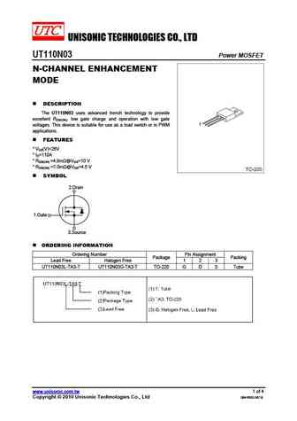
UNISONIC TECHNOLOGIES CO., LTD UT110N03 Power MOSFET N-CHANNEL ENHANCEMENT MODE DESCRIPTION The UT110N03 uses advanced trench technology to provide excellent RDS(ON), low gate charge and operation with low gate voltages. This device is suitable for use as a load switch or in PWM applications. FEATURES * VDS(V)=26V * ID=110A * RDS(ON) =4.8m @VGS=10 V * RDS(ON) =7.
mmbt1116.pdf
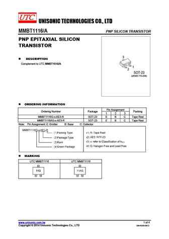
UNISONIC TECHNOLOGIES CO., LTD MMBT1116/A PNP SILICON TRANSISTOR PNP EPITAXIAL SILICON TRANSISTOR 3 DESCRIPTION Complement to UTC MMBT1616/A 1 2 SOT-23 (JEDEC TO-236) ORDERING INFORMATION Pin Assignment Ordering Number Package Packing 1 2 3 MMBT1116G-x-AE3-R SOT-23 E B C Tape Reel MMBT1116AG-x-AE3-R SOT-23 E B C Tape Reel Note Pin Assignment E Emitter B Ba
apt11gp60k.pdf
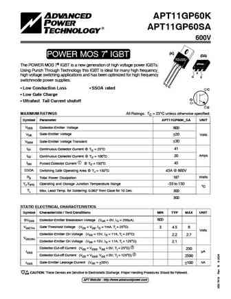
TYPICAL PERFORMANCE CURVES APT11GP60K_SA APT11GP60K APT11GP60SA 600V (K) POWER MOS 7 IGBT (SA) TO-220 D2PAK The POWER MOS 7 IGBT is a new generation of high voltage power IGBTs. Using Punch Through Technology this IGBT is ideal for many high frequency, C high voltage switching applications and has been optimized for high frequency G E switchmode power supplies. GC E L
apt11gf120krg.pdf

TYPICAL PERFORMANCE CURVES APT11GF120KR(G) 1200V APT11GF120KR APT11GF120KRG* *G Denotes RoHS Compliant, Pb Free Terminal Finish. FAST IGBT & FRED TO-220 The Fast IGBT is a new generation of high voltage power IGBTs. Using Non-Punch through technology, the Fast IGBT combined with an APT free wheeling Ultra Fast Recovery Epi- taxial Diode (FRED) offers superior ruggedness and fa
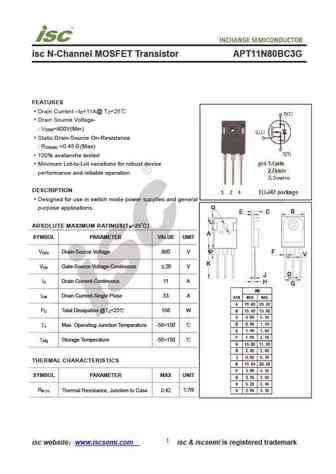
apt11n80bc3g.pdf

APT11N80BC3 800V 11A 0.45 Super Junction MOSFET TO-247 COOLMOS Power Semiconductors Ultra low RDS(ON) Low Miller Capacitance D Ultra Low Gate Charge, Qg Avalanche Energy Rated G TO-247 Package S MAXIMUM RATINGS All Ratings TC = 25 C unless otherwise specified. Symbol Parameter APT11N80BC3 UNIT VDSS Drain-Source Voltage 800 Volts ID
apt11gf120kr.pdf
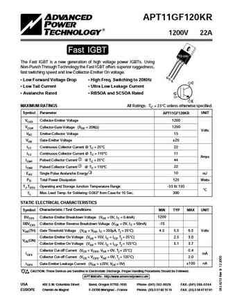
APT11GF120KR 1200V 22A Fast IGBT TO-220 The Fast IGBT is a new generation of high voltage power IGBTs. Using Non-Punch Through Technology the Fast IGBT offers superior ruggedness, fast switching speed and low Collector-Emitter On voltage. G C Low Forward Voltage Drop High Freq. Switching to 20KHz E C Low Tail Current Ultra Low Leakage Current Avalanche Rated
apt11gf120brd1.pdf
APT11GF120BRD1 1200V 22A Fast IGBT & FRED The Fast IGBT is a new generation of high voltage power IGBTs. Using Non- TO-247 Punch Through Technology the Fast IGBT combined with an APT free- wheeling ultraFast Recovery Epitaxial Diode (FRED) offers superior ruggedness and fast switching speed. G Low Forward Voltage Drop High Freq. Switching to 20KHz C E C Low Tail Cu
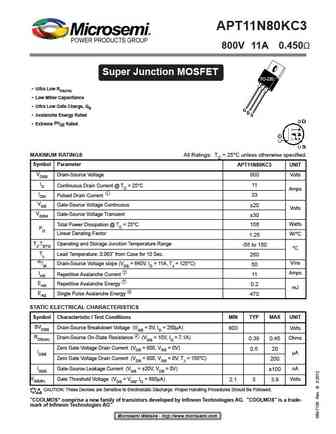
apt11n80bc3.pdf
APT11N80BC3 800V 11A 0.45 Super Junction MOSFET TO-247 COOLMOS Power Semiconductors Ultra low RDS(ON) Low Miller Capacitance D Ultra Low Gate Charge, Qg Avalanche Energy Rated G TO-247 Package S MAXIMUM RATINGS All Ratings TC = 25 C unless otherwise specified. Symbol Parameter APT11N80BC3 UNIT VDSS Drain-Source Voltage 800 Volts ID
apt11f80b apt11f80s.pdf
APT11F80B APT11F80S 600V, 12A, 0.9 Max trr 210ns N-Channel FREDFET POWER MOS 8 is a high speed, high voltage N-channel switch-mode power D3PAK MOSFET. This 'FREDFET' version has a drain-source (body) diode that has been opti- mized for high reliability in ZVS phase shifted bridge and other circuits through reduced trr, soft recovery, and high recovery dv/dt capability. Low
apt11n80kc3.pdf
APT11N80KC3 800V 11A 0.450 Super Junction MOSFET TO-220 COOLMOS Power Semiconductors Ultra low RDS(ON) G D S Low Miller Capacitance D Ultra Low Gate Charge, Qg Avalanche Energy Rated G TO-220 Package S MAXIMUM RATINGS All Ratings TC = 25 C unless otherwise specified. Symbol Parameter APT11N80KC3 UNIT VDSS Drain-Source Voltage 800
apt11gf120brdq1g.pdf
TYPICAL PERFORMANCE CURVES APT11GF120BRDQ1(G) 1200V APT11GF120BRDQ1 APT11GF120BRDQ1G* *G Denotes RoHS Compliant, Pb Free Terminal Finish. FAST IGBT & FRED The Fast IGBT is a new generation of high voltage power IGBTs. Using Non-Punch through technology, the Fast IGBT combined with an APT free wheeling Ultra Fast Recovery Epi- taxial Diode (FRED) offers superior ruggedness and f
apt11n80kc3g.pdf
APT11N80KC3 800V 11A 0.450 Super Junction MOSFET TO-220 Ultra Low RDS(ON) Low Miller Capacitance Ultra Low Gate Charge, Qg G D Avalanche Energy Rated S Extreme dv/dt Rated MAXIMUM RATINGS All Ratings TC = 25 C unless otherwise specified. Symbol Parameter APT11N80KC3 UNIT VDSS Drain-Source Voltage 800 Volts ID Continuous Drain Current @ TC = 25 C 1
apt11gp60bdqb.pdf
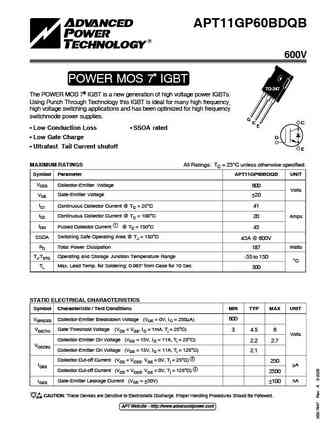
TYPICAL PERFORMANCE CURVES APT11GP60BDQB APT11GP60BDQB 600V POWER MOS 7 IGBT TO-247 The POWER MOS 7 IGBT is a new generation of high voltage power IGBTs. Using Punch Through Technology this IGBT is ideal for many high frequency, high voltage switching applications and has been optimized for high frequency switchmode power supplies. G C C E Low Conduction Loss SSOA rat
rt3t11m.pdf
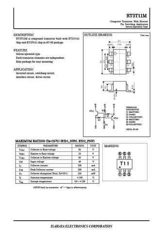
PRELIMINARY RT3T11M Composite Transistor With Resistor For Switching Application Silicon Epitaxial Type DESCRIPTION OUTLINE DRAWING Unit mm RT3T11M is compound transistor built with RT1N141 chip and RT1P141 chip in SC-88 package. FEATURE Silicon epitaxial type Each transistor elements are independent. Mini package for easy mounting APPLICATION Inverted circuit, switchin
sst108 sst109 sst110.pdf
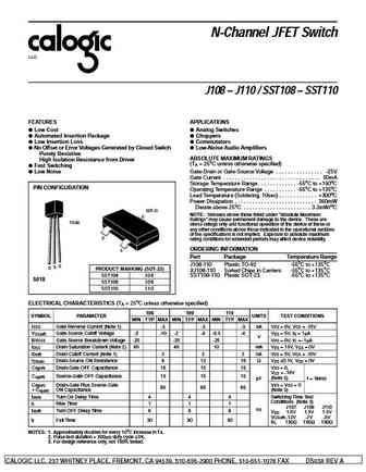
N-Channel JFET Switch LLC J108 J110 / SST108 SST110 FEATURES APPLICATIONS Low Cost Analog Switches Automated Insertion Package Choppers Low Insertion Loss Commutators No Offset or Error Voltages Generated by Closed Switch Low-Noise Audio Amplifiers Purely Resistive ABSOLUTE MAXIMUM RATINGS High Isolation
sst111 sst112 sst113.pdf
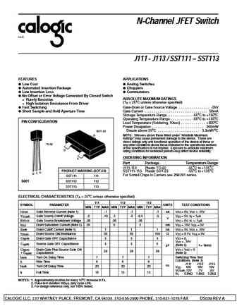
N-Channel JFET Switch LLC J111 - J113 / SST111 SST113 FEATURES APPLICATIONS Low Cost Analog Switches Automated Insertion Package Choppers Low Insertion Loss Commutators No Offset or Error Voltage Generated By Closed Switch ABSOLUTE MAXIMUM RATINGS Purely Resistive - (T = 25oC unless otherwise specified) A High Isola
ht117.pdf
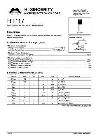
Spec. No. HT200207 HI-SINCERITY Issued Date 2002.04.01 Revised Date 2005.12.02 MICROELECTRONICS CORP. Page No. 1/4 HT117 PNP EPITAXIAL PLANAR TRANSISTOR Description TO-126 The HT117 is designed for use in general purpose amplifier and low-speed switching applications. Darlington Schematic C Absolute Maximum Ratings (TA=25 C) B Maximum Temperatures Storage Temperatu
ht112.pdf
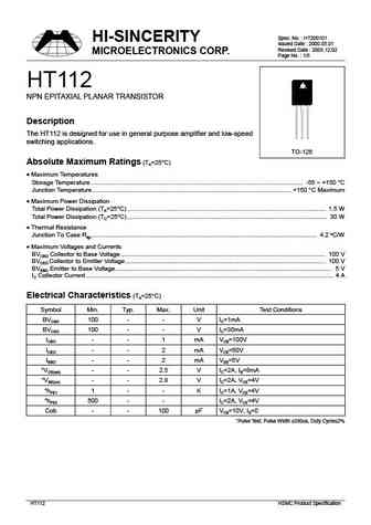
Spec. No. HT200101 HI-SINCERITY Issued Date 2000.05.01 Revised Date 2005.12.02 MICROELECTRONICS CORP. Page No. 1/5 HT112 NPN EPITAXIAL PLANAR TRANSISTOR Description The HT112 is designed for use in general purpose amplifier and low-speed switching applications. TO-126 Absolute Maximum Ratings (TA=25 C) Maximum Temperatures Storage Temperature .........................
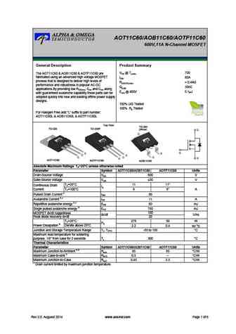
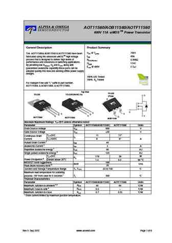
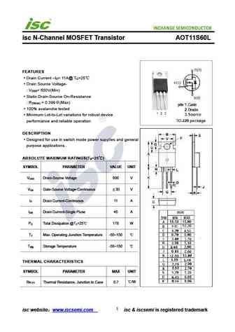
aot11s65.pdf

AOT11S65/AOB11S65/AOTF11S65 TM 650V 11A MOS Power Transistor General Description Product Summary VDS @ Tj,max 750V The AOT11S65 & AOB11S65 & AOTF11S65 have been fabricated using the advanced MOSTM high voltage IDM 45A process that is designed to deliver high levels of RDS(ON),max 0.399 performance and robustness in switching applications. Qg,typ 13.2nC By provi
aot1100l.pdf
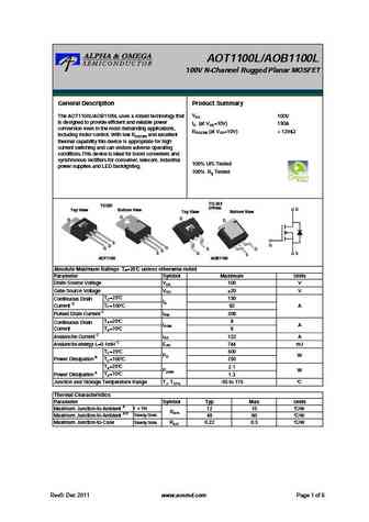
AOT1100L/AOB1100L 100V N-Channel Rugged Planar MOSFET General Description Product Summary VDS 100V The AOT1100L/AOB1100L uses a robust technology that is designed to provide efficient and reliable power ID (at VGS=10V) 130A conversion even in the most demanding applications, RDS(ON) (at VGS=10V)
aot11s60l aob11s60l aotf11s60l aotf11s60.pdf
AOT11S60L/AOB11S60L/AOTF11S60L/AOTF11S60 TM 600V 11A a MOS Power Transistor General Description Product Summary VDS @ Tj,max 700V The AOT11S60L & AOB11S60L & AOTF11S60L & AOTF11S60 have been fabricated using the advanced IDM 45A aMOSTM high voltage process that is designed to deliver high RDS(ON),max 0.399W levels of performance and robustness in switching applications. Qg,typ 11
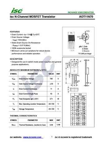
aot11n70.pdf
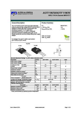
AOT11N70/AOTF11N70 700V,11A N-Channel MOSFET General Description Product Summary VDS 800V@150 The AOT11N70 & AOTF11N70 have been fabricated using an advanced high voltage MOSFET process that is ID (at VGS=10V) 11A designed to deliver high levels of performance and RDS(ON) (at VGS=10V)
aot11s65 aob11s65 aotf11s65.pdf
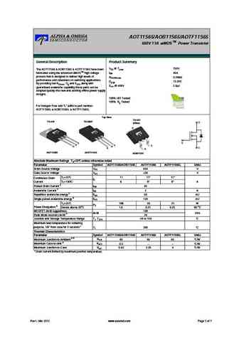
AOT11S65/AOB11S65/AOTF11S65 TM 650V 11A MOS Power Transistor General Description Product Summary VDS @ Tj,max 750V The AOT11S65 & AOB11S65 & AOTF11S65 have been fabricated using the advanced MOSTM high voltage IDM 45A process that is designed to deliver high levels of RDS(ON),max 0.399 performance and robustness in switching applications. Qg,typ 13.2nC By provi
aot11c60.pdf
AOT11C60/AOB11C60/AOTF11C60 600V,11A N-Channel MOSFET General Description Product Summary VDS @ Tj,max 700 The AOT11C60 & AOB11C60 & AOTF11C60 are fabricated using an advanced high voltage MOSFET IDM 80A process that is designed to deliver high levels of RDS(ON),max
aot11s60l.pdf
AOT11S60/AOB11S60/AOTF11S60 TM 600V 11A MOS Power Transistor General Description Product Summary VDS @ Tj,max 700V The AOT11S60& AOB11S60 & AOTF11S60 have been fabricated using the advanced MOSTM high voltage IDM 45A process that is designed to deliver high levels of RDS(ON),max 0.399 performance and robustness in switching applications. Qg,typ 11nC By providin
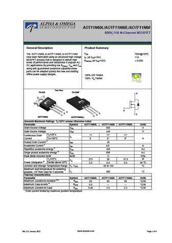
aot11n60.pdf
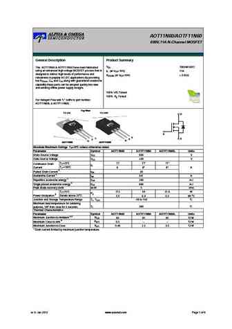
AOT11N60/AOTF11N60 600V,11A N-Channel MOSFET General Description Product Summary VDS The AOT11N60 & AOTF11N60 have been fabricated 700V@150 using an advanced high voltage MOSFET process that is ID (at VGS=10V) 11A designed to deliver high levels of performance and RDS(ON) (at VGS=10V)
aot11s60.pdf

AOT11S60/AOB11S60/AOTF11S60 TM 600V 11A MOS Power Transistor General Description Product Summary VDS @ Tj,max 700V The AOT11S60& AOB11S60 & AOTF11S60 have been fabricated using the advanced MOSTM high voltage IDM 45A process that is designed to deliver high levels of RDS(ON),max 0.399 performance and robustness in switching applications. Qg,typ 11nC By providin
aot11n60l aotf11n60l aotf11n60.pdf
AOT11N60L/AOTF11N60L/AOTF11N60 600V,11A N-Channel MOSFET General Description Product Summary VDS The AOT11N60L & AOTF11N60L & AOTF11N60 700V@150 have been fabricated using an advanced high voltage ID (at VGS=10V) 11A MOSFET process that is designed to deliver high RDS(ON) (at VGS=10V)
aot11s65l.pdf

AOT11S65/AOB11S65/AOTF11S65 TM 650V 11A MOS Power Transistor General Description Product Summary VDS @ Tj,max 750V The AOT11S65 & AOB11S65 & AOTF11S65 have been fabricated using the advanced MOSTM high voltage IDM 45A process that is designed to deliver high levels of RDS(ON),max 0.399 performance and robustness in switching applications. Qg,typ 13.2nC By provi
ap95t11gi-hf.pdf
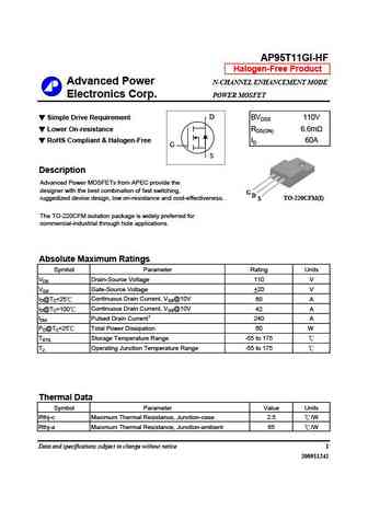
AP95T11GI-HF Halogen-Free Product Advanced Power N-CHANNEL ENHANCEMENT MODE Electronics Corp. POWER MOSFET Simple Drive Requirement D BVDSS 110V Lower On-resistance RDS(ON) 6.6m RoHS Compliant & Halogen-Free ID 60A G S Description Advanced Power MOSFETs from APEC provide the designer with the best combination of fast switching, G D TO-220CFM(I) ruggedized device de
kzt1149a.pdf
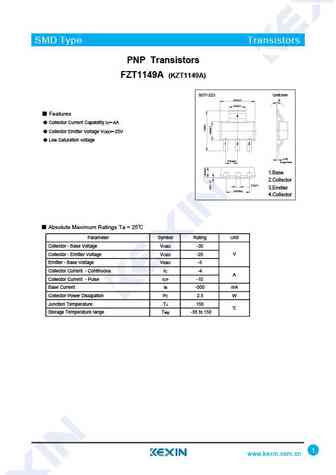
SMD Type Transistors PNP Transistors FZT1149A (KZT1149A) Unit mm SOT-223 6.50 0.2 3.00 0.1 Features 4 Collector Current Capability IC=-4A Collector Emitter Voltage VCEO=-25V Low Saturation voltage 1 2 3 0.250 2.30 (typ) Gauge Plane 1.Base 2.Collector 0.70 0.1 3.Emitter 4.60 (typ) 4.Collector Absolute Maximum Ratings Ta = 25 Parameter Symbol
fzt1151a.pdf
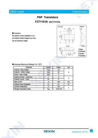
SMD Type Transistors PNP Transistors FZT1151A (KZT1151A) Unit mm SOT-223 6.50 0.2 3.00 0.1 4 Features Collector Current Capability IC=-3A Collector Emitter Voltage VCEO=-40V Low Saturation voltage 1 2 3 0.250 2.30 (typ) Gauge Plane 1.Base 2.Collector 0.70 0.1 3.Emitter 4.60 (typ) 4.Collector Absolute Maximum Ratings Ta = 25 Parameter Symbol R
kzt1151a.pdf

SMD Type Transistors PNP Transistors FZT1151A (KZT1151A) Unit mm SOT-223 6.50 0.2 3.00 0.1 4 Features Collector Current Capability IC=-3A Collector Emitter Voltage VCEO=-40V Low Saturation voltage 1 2 3 0.250 2.30 (typ) Gauge Plane 1.Base 2.Collector 0.70 0.1 3.Emitter 4.60 (typ) 4.Collector Absolute Maximum Ratings Ta = 25 Parameter Symbol R
ndt110n03.pdf
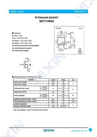
SMD Type MOSFET N-Channel MOSFET NDT110N03 TO-252 Unit mm +0.15 6.50-0.15 +0.1 2.30 -0.1 +0.2 Features 5.30-0.2 +0.8 0.50 -0.7 VDS (V) = 30V 4 ID = 110 A (VGS = 10V) RDS(ON) 4m (VGS = 10V) 0.127 +0.1 0.80-0.1 max RDS(ON) 6m (VGS = 4.5V) High Power and current handing capability + 0.1 Lead free product is acquired 2.3 0.60- 0
fzt1149a.pdf

SMD Type Transistors PNP Transistors FZT1149A (KZT1149A) Unit mm SOT-223 6.50 0.2 3.00 0.1 Features 4 Collector Current Capability IC=-4A Collector Emitter Voltage VCEO=-25V Low Saturation voltage 1 2 3 0.250 2.30 (typ) Gauge Plane 1.Base 2.Collector 0.70 0.1 3.Emitter 4.60 (typ) 4.Collector Absolute Maximum Ratings Ta = 25 Parameter Symbol
cht1198gp.pdf
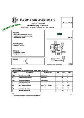
CHENMKO ENTERPRISE CO.,LTD CHT1198GP SURFACE MOUNT PNP Switching Transistor VOLTAGE 80 Volts CURRENT 0.5 Ampere FEATURE * Small surface mounting type. (SOT-23) * Low Collector-Emitter saturation voltage. * High breakdown voltage. SOT-23 CONSTRUCTION (1) * PNP Silicon Transistor (3) (2) MARKING ( ) ( ) .055 1.40 .028 0.70 * J22 @hFE as Q Grade ( ) ( ) .047 1.20 .020 0.50 (
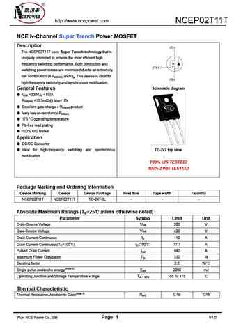
ncep12t11.pdf
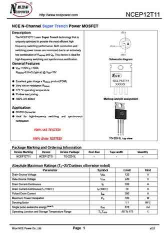
http //www.ncepower.com NCEP12T11 NCE N-Channel Super Trench Power MOSFET Description The NCEP12T11 uses Super Trench technology that is uniquely optimized to provide the most efficient high frequency switching performance. Both conduction and switching power losses are minimized due to an extremely low combination of RDS(ON) and Qg. This device is ideal for high-frequency swit
ncep01t11d.pdf
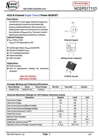
Pb Free Product http //www.ncepower.com NCEP01T11D NCE N-Channel Super Trench Power MOSFET Description The NCEP01T11D uses Super Trench technology that is uniquely optimized to provide the most efficient high frequency switching performance. Both conduction and switching power losses are minimized due to an extremely low combination of RDS(ON) and Qg. This device is ideal for
ncep01t11.pdf
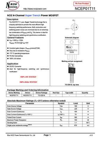
Pb Free Product http //www.ncepower.com NCEP01T11 NCE N-Channel Super Trench Power MOSFET Description The NCEP01T11 uses Super Trench technology that is uniquely optimized to provide the most efficient high frequency switching performance. Both conduction and switching power losses are minimized due to an extremely low combination of RDS(ON) and Qg. This device is ideal for hi
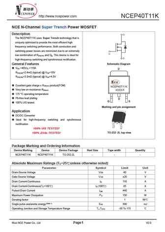
ncep40t11.pdf
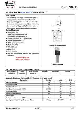
http //www.ncepower.com NCEP40T11 NCE N-Channel Super Trench Power MOSFET Description The NCEP40T11 uses Super Trench technology that is uniquely optimized to provide the most efficient high frequency switching performance. Both conduction and switching power losses are minimized due to an extremely low combination of RDS(ON) and Qg. This device is ideal for high-frequency swi
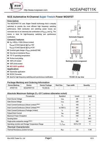
nceap40t11ak.pdf
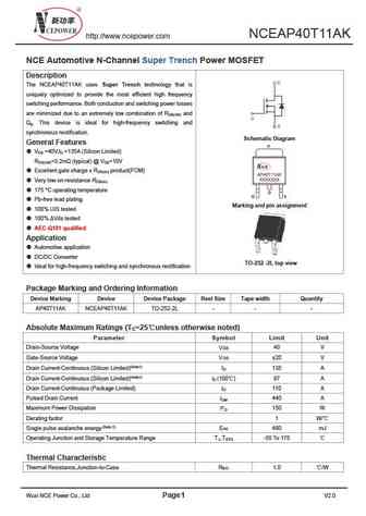
NCEAP40T11AK http //www.ncepower.com NCE Automotive N-Channel Super Trench Power MOSFET Description The NCEAP40T11AK uses Super Trench technology that is uniquely optimized to provide the most efficient high frequency switching performance. Both conduction and switching power losses are minimized due to an extremely low combination of R and DS(ON) Q . This device is ideal for high-freq
nceap40t11k.pdf
NCEAP40T11K http //www.ncepower.com NCE Automotive N-Channel Super Trench Power MOSFET Description The NCEAP40T11K uses Super Trench technology that is uniquely optimized to provide the most efficient high frequency switching performance. Both conduction and switching power losses are minimized due to an extremely low combination of R and Q . This DS(ON) g device is ideal for high-freq
ncep02t11d.pdf
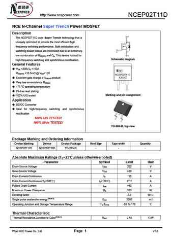
http //www.ncepower.com NCEP02T11D NCE N-Channel Super Trench Power MOSFET Description The NCEP02T11D uses Super Trench technology that is uniquely optimized to provide the most efficient high frequency switching performance. Both conduction and switching power losses are minimized due to an extremely low combination of RDS(ON) and Qg. This device is ideal for Schematic diagram
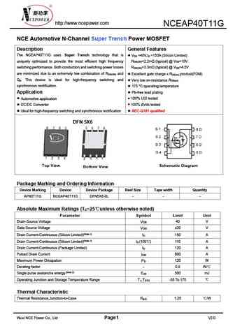
nceap40t11ag.pdf
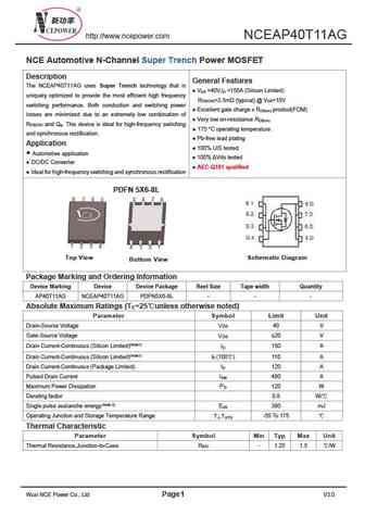
http //www.ncepower.com NCEAP40T11AG NCE Automotive N-Channel Super Trench Power MOSFET Description General Features The NCEAP40T11AG uses Super Trench technology that is V =40V,I =150A (Silicon Limited) DS D uniquely optimized to provide the most efficient high frequency R =2.5m (typical) @ V =10V DS(ON) GS switching performance. Both conduction and switching power Excell
ncep40t11ak.pdf
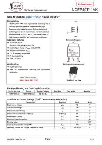
Pb Free Product http //www.ncepower.com NCEP40T11AK NCE N-Channel Super Trench Power MOSFET Description The NCEP40T11AK uses Super Trench technology that is uniquely optimized to provide the most efficient high frequency switching performance. Both conduction and switching power losses are minimized due to an extremely low combination of R and Q . This device is ideal for DS(ON) g hig
ncep40t11k.pdf
http //www.ncepower.com NCEP40T11K NCE N-Channel Super Trench Power MOSFET Description The NCEP40T11K uses Super Trench technology that is uniquely optimized to provide the most efficient high frequency switching performance. Both conduction and switching power losses are minimized due to an extremely low combination of R and Q . This device is ideal for DS(ON) g high-frequency switch
ncep40t11ag.pdf
Pb Free Product http //www.ncepower.com NCEP40T11AG NCE N-Channel Super Trench Power MOSFET Description The NCEP40T11AG uses Super Trench technology that is uniquely optimized to provide the most efficient high frequency switching performance. Both conduction and switching power losses are minimized due to an extremely low combination of RDS(ON) and Qg. This device is ideal for
ncep85t11.pdf
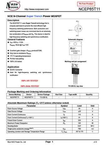
Pb Free Product http //www.ncepower.com NCEP85T11 NCE N-Channel Super Trench Power MOSFET Description The NCEP85T11 uses Super Trench technology that is uniquely optimized to provide the most efficient high frequency switching performance. Both conduction and switching power losses are minimized due to an extremely low combination of RDS(ON) and Qg. This device is ideal for hi
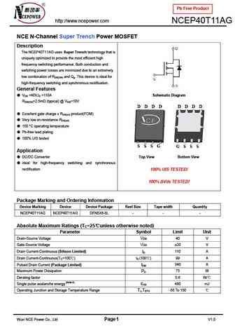
ncep40t11g.pdf
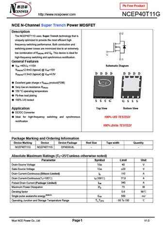
Pb Free Product http //www.ncepower.com NCEP40T11G NCE N-Channel Super Trench Power MOSFET Description The NCEP40T11G uses Super Trench technology that is uniquely optimized to provide the most efficient high frequency switching performance. Both conduction and switching power losses are minimized due to an extremely low combination of RDS(ON) and Qg. This device is ideal for
ncep02t11t.pdf
http //www.ncepower.com NCEP02T11T NCE N-Channel Super Trench Power MOSFET Description The NCEP02T11T uses Super Trench technology that is uniquely optimized to provide the most efficient high frequency switching performance. Both conduction and switching power losses are minimized due to an extremely low combination of RDS(ON) and Qg. This device is ideal for high-frequency sw
but11apx.pdf

INCHANGE Semiconductor isc Product Specification isc Silicon NPN Power Transistor BUT11APX DESCRIPTION High Voltage High Speed Switching APPLICATIONS Converters Inverters Switching regulators Motor control systems ABSOLUTE MAXIMUM RATINGS (Ta=25 ) SYMBOL PARAMETER VALUE UNIT VCES Collector-Emitter Voltage VBE= 0 1000 V VCEO Collector-Emitter Voltage 450
aot11s65.pdf

isc N-Channel MOSFET Transistor AOT11S65 FEATURES Drain Current I =11A@ T =25 D C Drain Source Voltage- V =650V(Min) DSS Static Drain-Source On-Resistance R = 0.399 (Max) DS(on) 100% avalanche tested Minimum Lot-to-Lot variations for robust device performance and reliable operation DESCRIPTION Designed for use in switch mode power supplies and general purpo
but11ai.pdf
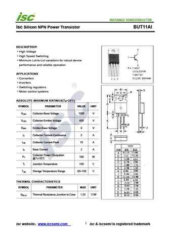
isc Silicon NPN Power Transistor BUT11AI DESCRIPTION High Voltage High Speed Switching Minimum Lot-to-Lot variations for robust device performance and reliable operation APPLICATIONS Converters Inverters Switching regulators Motor control systems ABSOLUTE MAXIMUM RATINGS(T =25 ) a SYMBOL PARAMETER VALUE UNIT V Collector-Base Voltage 1000 V CBO V Collector-Emitter
aot1100l.pdf

isc N-Channel MOSFET Transistor AOT1100L FEATURES Drain Current I = 130A@ T =25 D C Drain Source Voltage- V = 100V(Min) DSS Static Drain-Source On-Resistance R = 12m (Max) DS(on) 100% avalanche tested Minimum Lot-to-Lot variations for robust device performance and reliable operation DESCRIPTION Designed for use in switch mode power supplies and general purp
apt11n80bc3g.pdf
isc N-Channel MOSFET Transistor APT11N80BC3G FEATURES Drain Current I =11A@ T =25 D C Drain Source Voltage- V =800V(Min) DSS Static Drain-Source On-Resistance R =0.45 (Max) DS(on) 100% avalanche tested Minimum Lot-to-Lot variations for robust device performance and reliable operation DESCRIPTION Designed for use in switch mode power supplies and general pur
but11fi.pdf
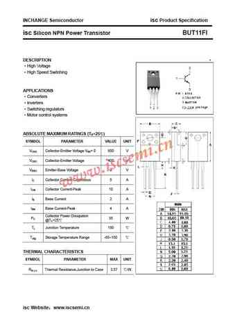
INCHANGE Semiconductor isc Product Specification isc Silicon NPN Power Transistor BUT11FI DESCRIPTION High Voltage High Speed Switching APPLICATIONS Converters Inverters Switching regulators Motor control systems ABSOLUTE MAXIMUM RATINGS (Ta=25 ) SYMBOL PARAMETER VALUE UNIT VCES Collector-Emitter Voltage VBE= 0 850 V VCEO Collector-Emitter Voltage 400 V
aot11n70.pdf
isc N-Channel MOSFET Transistor AOT11N70 FEATURES Drain Current I = 11A@ T =25 D C Drain Source Voltage- V = 700V(Min) DSS Static Drain-Source On-Resistance R = 0.87 (Max) DS(on) 100% avalanche tested Minimum Lot-to-Lot variations for robust device performance and reliable operation DESCRIPTION Designed for use in switch mode power supplies and general purp
but11a.pdf
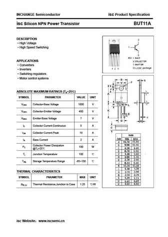
INCHANGE Semiconductor isc Product Specification isc Silicon NPN Power Transistor BUT11A DESCRIPTION High Voltage High Speed Switching APPLICATIONS Converters Inverters Switching regulators Motor control systems ABSOLUTE MAXIMUM RATINGS (Ta=25 ) SYMBOL PARAMETER VALUE UNIT VCBO Collector-Base Voltage 1000 V VCEO Collector-Emitter Voltage 450 V VEBO Emitt
but11afi.pdf
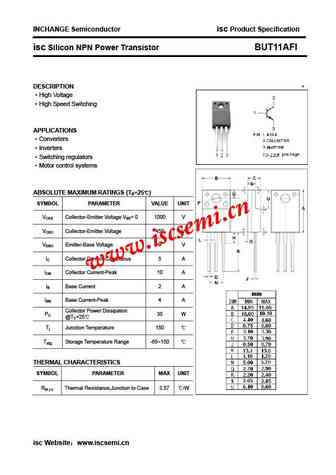
INCHANGE Semiconductor isc Product Specification isc Silicon NPN Power Transistor BUT11AFI DESCRIPTION High Voltage High Speed Switching APPLICATIONS Converters Inverters Switching regulators Motor control systems ABSOLUTE MAXIMUM RATINGS (Ta=25 ) SYMBOL PARAMETER VALUE UNIT VCES Collector-Emitter Voltage VBE= 0 1000 V VCEO Collector-Emitter Voltage 450
aot11s60l.pdf
isc N-Channel MOSFET Transistor AOT11S60L FEATURES Drain Current I = 11A@ T =25 D C Drain Source Voltage- V = 600V(Min) DSS Static Drain-Source On-Resistance R = 0.399 (Max) DS(on) 100% avalanche tested Minimum Lot-to-Lot variations for robust device performance and reliable operation DESCRIPTION Designed for use in switch mode power supplies and general pu
aot11n60.pdf

isc N-Channel MOSFET Transistor AOT11N60 FEATURES Drain Current I = 11A@ T =25 D C Drain Source Voltage- V = 600V(Min) DSS Static Drain-Source On-Resistance R = 0.7 (Max) DS(on) 100% avalanche tested Minimum Lot-to-Lot variations for robust device performance and reliable operation DESCRIPTION Designed for use in switch mode power supplies and general purpo
but11.pdf
INCHANGE Semiconductor isc Product Specification isc Silicon NPN Power Transistor BUT11 DESCRIPTION High Voltage High Speed Switching APPLICATIONS Converters Inverters Switching regulators Motor control systems ABSOLUTE MAXIMUM RATINGS (Ta=25 ) SYMBOL PARAMETER VALUE UNIT VCBO Collector-Base Voltage 850 V VCEO Collector-Emitter Voltage 400 V VEBO Emitter
but11af.pdf
INCHANGE Semiconductor isc Product Specification isc Silicon NPN Power Transistor BUT11AF DESCRIPTION High Voltage High Speed Switching APPLICATIONS Converters Inverters Switching regulators Motor control systems ABSOLUTE MAXIMUM RATINGS (Ta=25 ) SYMBOL PARAMETER VALUE UNIT VCBO Collector-Base Voltage 1000 V VCEO Collector-Emitter Voltage 450 V VEBO Em
apt11f80b.pdf
isc N-Channel MOSFET Transistor APT11F80B FEATURES Drain Current I = 12A@ T =25 D C Drain Source Voltage- V =800V(Min) DSS Static Drain-Source On-Resistance R = 0.9 (Max) DS(on) 100% avalanche tested Minimum Lot-to-Lot variations for robust device performance and reliable operation DESCRIPTION Designed for use in switch mode power supplies and general purpo
Другие транзисторы: KTC4075-GR, KTC4075-O, KTC4075-Y, KTC4347, KTC4373-O, KTC4373-Y, T03N100GP, T10N60GP, 2SD313, TFH1036, TFH1037, TFH2411, TFH2412, TFH2444, TFH45, TFJD1760, TTC004B
Параметры биполярного транзистора и их взаимосвязь

Список транзисторов
Обновления
BJT: ZDT6705 | GA1L4Z | GA1A4M | SBT42 | 2SA200-Y | 2SA200-O | 2SD882-Q | 2SD882-P | 2SD882-E | 2SC945-L | 2SC945-H | 2SC4226-R23 | 2SC3357-F | 2SC3357-E | 2SC3356-R26 | 2SC3356-R24 | 2SC3356-R23 | 2SB772-Q | 2SB772-P | 2SB772-E | 2SA1015-L
Popular searches
2sc2389 | b331 transistor | 2sa720 | 2sc1345 | 2sd555 | a950 transistor | k2611 | c1740 transistor