2SC1894 Datasheet. Specs and Replacement
Type Designator: 2SC1894 📄📄
Material of Transistor: Si
Polarity: NPN
Absolute Maximum Ratings
Maximum Collector Power Dissipation (Pc): 50 W
Maximum Collector-Base Voltage |Vcb|: 1500 V
Maximum Collector-Emitter Voltage |Vce|: 600 V
Maximum Emitter-Base Voltage |Veb|: 5 V
Maximum Collector Current |Ic max|: 6 A
Max. Operating Junction Temperature (Tj): 150 °C
Electrical Characteristics
Transition Frequency (ft): 1.5 MHz
Forward Current Transfer Ratio (hFE), MIN: 8
Package: TO3
2SC1894 Substitution
- BJT ⓘ Cross-Reference Search
2SC1894 datasheet
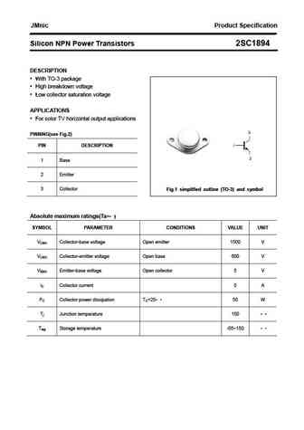
JMnic Product Specification Silicon NPN Power Transistors 2SC1894 DESCRIPTION With TO-3 package High breakdown voltage Low collector saturation voltage APPLICATIONS For color TV horizontal output applications PINNING(see Fig.2) PIN DESCRIPTION 1 Base 2 Emitter 3 Collector Fig.1 simplified outline (TO-3) and symbol Absolute maximum ratings(Ta= ) SYMBOL PARAME... See More ⇒

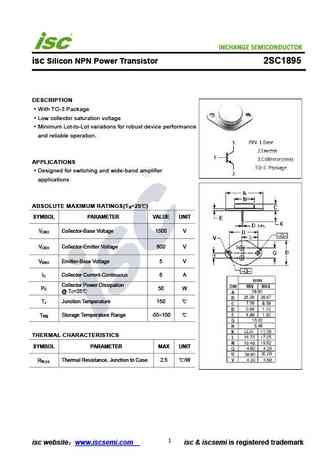
INCHANGE Semiconductor isc Silicon NPN Power Transistor 2SC1894 DESCRIPTION With TO-3 Package Low collector saturation voltage Minimum Lot-to-Lot variations for robust device performance and reliable operation. APPLICATIONS Designed for switching and wide-band amplifier applications ABSOLUTE MAXIMUM RATINGS(T =25 ) a SYMBOL PARAMETER VALUE UNIT V Collector-Base Voltage 15... See More ⇒
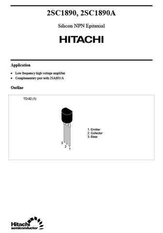
2SC1890, 2SC1890A Silicon NPN Epitaxial Application Low frequency high voltage amplifier Complementary pair with 2SA893/A Outline TO-92 (1) 1. Emitter 2. Collector 3. Base 3 2 1 2SC1890, 2SC1890A Absolute Maximum Ratings (Ta = 25 C) Ratings Item Symbol 2SC1890 2SC1890A Unit Collector to base voltage VCBO 90 120 V Collector to emitter voltage VCEO 90 120 V Emitter to... See More ⇒
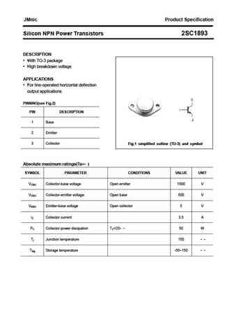
JMnic Product Specification Silicon NPN Power Transistors 2SC1893 DESCRIPTION With TO-3 package High breakdown voltage APPLICATIONS For line-operated horizontal deflection output applications PINNING(see Fig.2) PIN DESCRIPTION 1 Base 2 Emitter 3 Collector Fig.1 simplified outline (TO-3) and symbol Absolute maximum ratings(Ta= ) SYMBOL PARAMETER CONDITIONS VAL... See More ⇒

Detailed specifications: 2SC1888, 2SC1889, 2SC189, 2SC1890, 2SC1890A, 2SC1891, 2SC1892, 2SC1893, TIP122, 2SC1895, 2SC1896, 2SC1897, 2SC1898, 2SC1899, 2SC19, 2SC190, 2SC1900
Keywords - 2SC1894 pdf specs
2SC1894 cross reference
2SC1894 equivalent finder
2SC1894 pdf lookup
2SC1894 substitution
2SC1894 replacement
🌐 : EN ES РУ

LIST
Last Update
BJT: GA1A4M | SBT42 | 2SA200-Y | 2SA200-O | 2SD882-Q | 2SD882-P
Popular searches
2n3053 | a1015 | mpsa42 | 2n5551 transistor | a1015 transistor | c945 | ac128 transistor | 2n3055 transistor