2SD2110 Specs and Replacement
Type Designator: 2SD2110
Material of Transistor: Si
Polarity: NPN
Absolute Maximum Ratings
Maximum Collector Power Dissipation (Pc): 25 W
Maximum Collector-Base Voltage |Vcb|: 80 V
Maximum Collector-Emitter Voltage |Vce|: 80 V
Maximum Emitter-Base Voltage |Veb|: 7 V
Maximum Collector Current |Ic max|: 4 A
Max. Operating Junction Temperature (Tj): 150 °C
Electrical Characteristics
Forward Current Transfer Ratio (hFE), MIN: 12000
Noise Figure, dB: -
Package: TO220FM
- BJT ⓘ Cross-Reference Search
2SD2110 datasheet
..1. Size:198K inchange semiconductor
2sd2110.pdf 
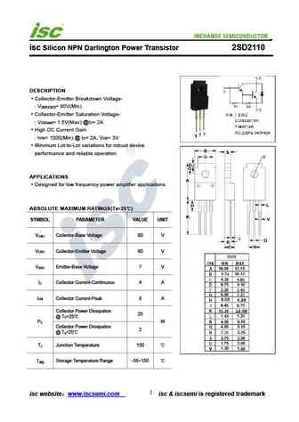
isc Silicon NPN Darlington Power Transistor 2SD2110 DESCRIPTION Collector-Emitter Breakdown Voltage- V = 80V(Min) (BR)CEO Collector-Emitter Saturation Voltage- V = 1.5V(Max) @I = 2A CE(sat) C High DC Current Gain h = 1000(Min) @ I = 2A, V = 3V FE C CE Minimum Lot-to-Lot variations for robust device performance and reliable operation APPLICATIONS Designed for low fr... See More ⇒
8.1. Size:67K sanyo
2sd2117.pdf 

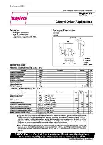
Ordering number EN3204 NPN Epitaxial Planar Silicon Transistor 2SD2117 General Driver Applications Features Package Dimensions Darlington connection. unit mm High DC current gain. 2064A Large current capacity, wide ASO. [2SD2117] 2.5 1.45 6.9 1.0 0.6 0.9 0.5 1 2 3 0.45 1 Emitter 2 Collector 3 Base 2.54 2.54 SANYO NMP Specifications Absolute Maximum Ra... See More ⇒
8.2. Size:74K sanyo
2sd2116.pdf 

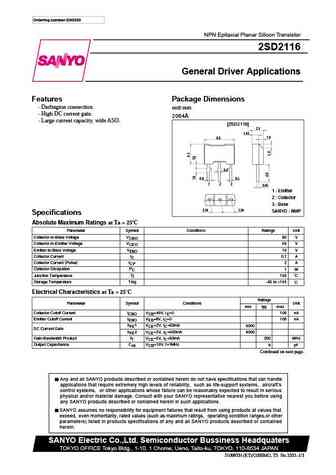
Ordering number EN3203 NPN Epitaxial Planar Silicon Transistor 2SD2116 General Driver Applications Features Package Dimensions Darlington connection. unit mm High DC current gain. 2064A Large current capacity, wide ASO. [2SD2116] 2.5 1.45 6.9 1.0 0.6 0.9 0.5 1 2 3 0.45 1 Emitter 2 Collector 3 Base 2.54 2.54 SANYO NMP Specifications Absolute Maximum Ra... See More ⇒
8.3. Size:157K rohm
2sd2114ks.pdf 

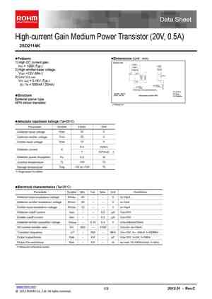
High-current Gain Medium Power Transistor (20V, 0.5A) 2SD2114K Features Dimensions (Unit mm) 1) High DC current gain. 2SD2114K 2.9 0.2 1.1+0.2 hFE = 1200 (Typ.) 1.9 0.2 -0.1 0.8 0.1 0.95 0.95 2) High emitter-base voltage. (1) (2) VEBO =12V (Min.) 0 0.1 3) Low VCE (sat). VCE (sat) = 0.18V (Typ.) (3) (IC / IB = 500mA / 20mA) +0.1 0.15-0.06 +0.1 0.4 -0... See More ⇒
8.4. Size:87K rohm
2sd2098 2sd2118 2sd2097.pdf 

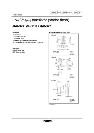
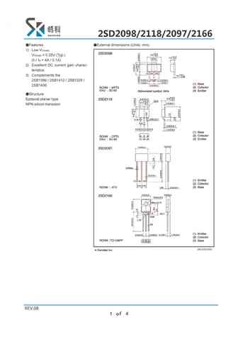
2SD2098 / 2SD2118 / 2SD2097 Transistors Low VCE(sat) transistor (strobe flash) 2SD2098 / 2SD2118 / 2SD2097 External dimensions (Units mm) Features 1) Low VCE(sat). 2SD2098 +0.2 VCE(sat) = 0.25V (Typ.) 4.5 -0.1 +0.2 1.5 1.6 0.1 -0.1 (IC/IB = 4A / 0.1A) 2) Excellent DC current gain characteristics. 3) Complements the 2SB1386 / 2SB1412 / 2SB1326. (1) (2) (3) 0.4+0.1 -0.05 ... See More ⇒
8.5. Size:124K rohm
2sd2114.pdf 

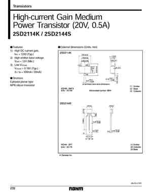
Transistors High-current Gain Medium Power Transistor (20V, 0.5A) 2SD2114K / 2SD2144S FFeatures FExternal dimensions (Units mm) 1) High DC current gain. hFE = 1200 (Typ.) 2) High emitter-base voltage. VEBO = 12V (Min.) 3) Low VCE(sat). VCE(sat) = 0.18V (Typ.) (IC / IB = 500mA / 20mA) FStructure Epitaxial planar type NPN silicon transistor (96-232-C107) 232 Transistors 2SD211... See More ⇒
8.6. Size:89K rohm
2sd2114k-s.pdf 

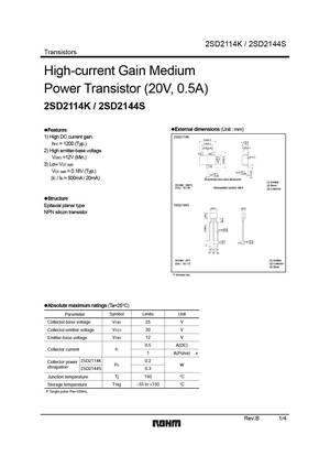
2SD2114K / 2SD2144S Transistors High-current Gain Medium Power Transistor (20V, 0.5A) 2SD2114K / 2SD2144S External dimensions (Unit mm) Features 1) High DC current gain. 2SD2114K 2.9 0.2 1.1+0.2 1.9 0.2 -0.1 hFE = 1200 (Typ.) 0.8 0.1 0.95 0.95 2) High emitter-base voltage. (1) (2) 0 0.1 VEBO =12V (Min.) 3) Low VCE (sat). (3) +0.1 VCE (sat) = 0.18V (Ty... See More ⇒
8.7. Size:89K rohm
2sd2114k 2sd2144s.pdf 

2SD2114K / 2SD2144S Transistors High-current Gain Medium Power Transistor (20V, 0.5A) 2SD2114K / 2SD2144S External dimensions (Unit mm) Features 1) High DC current gain. 2SD2114K 2.9 0.2 1.1+0.2 1.9 0.2 -0.1 hFE = 1200 (Typ.) 0.8 0.1 0.95 0.95 2) High emitter-base voltage. (1) (2) 0 0.1 VEBO =12V (Min.) 3) Low VCE (sat). (3) +0.1 VCE (sat) = 0.18V (Ty... See More ⇒
8.8. Size:31K hitachi
2sd2115.pdf 

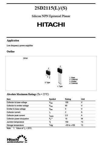
2SD2115(L)/(S) Silicon NPN Epitaxial Planar Application Low frequency power amplifier Outline DPAK 4 4 1 2 1. Base 3 2. Collector 3. Emitter S Type 12 4. Collector 3 L Type Absolute Maximum Ratings (Ta = 25 C) Item Symbol Rating Unit Collector to base voltage VCBO 150 V Collector to emitter voltage VCEO 60 V Emitter to base voltage VEBO 5V Collector current IC 2A Colle... See More ⇒
8.9. Size:250K secos
2sd2114.pdf 

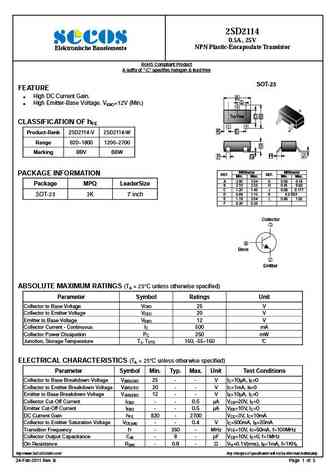
2SD2114 0.5A , 25V NPN Plastic-Encapsulate Transistor Elektronische Bauelemente RoHS Compliant Product A suffix of -C specifies halogen & lead-free SOT-23 FEATURE High DC Current Gain. A L High Emitter-Base Voltage. VEBO=12V (Min.) 3 3 Top View C B CLASSIFICATION OF hFE 1 1 2 2 K E Product-Rank 2SD2114-V 2SD2114-W Range 820 1800 1200 2700 D Marking BBV ... See More ⇒
8.10. Size:70K secos
2sd2118.pdf 

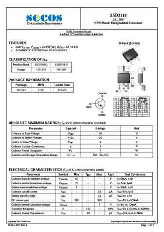
2SD2118 5A , 50V NPN Plastic Encapsulated Transistor Elektronische Bauelemente RoHS Compliant Product A suffix of -C specifies halogen & lead-free FEATURES D-Pack (TO-252) Low VCE(sat). VCE(sat) = 0.25V(Typ.) (IC/IB = 4A / 0.1A) Excellent DC Current Gain Characteristics CLASSIFICATION OF hFE Product-Rank 2SD2118-Q 2SD2118-R A C B D Range 120 270 180 390 G E... See More ⇒
8.11. Size:883K htsemi
2sd2114.pdf 

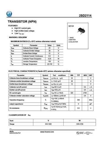
2SD2114 TRANSISTOR (NPN) FEATURES SOT-23 High DC current gain. High emitter-base voltage. Low VCE (sat). MARKING BBV,BBW 1. BASE 2.EMITTER MAXIMUM RATINGS (TA=25 unless otherwise noted) 3.COLLECTOR Symbol Parameter Value Units VCBO Collector-Base Voltage 25 V VCEO Collector-Emitter Voltage 20 V VEBO Emitter-Base Voltage 12 V IC Collector Current -Continuou... See More ⇒
8.12. Size:210K lge
2sd2118.pdf 

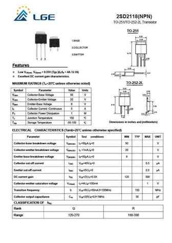
2SD2118(NPN) TO-251/TO-252-2L Transistor TO-251 1.BASE 2.COLLECTOR 3.EMITTER 1 2 3 Features Low VCE(sat). VCE(sat) = 0.25V (Typ.)(IC/IB = 4A / 0.1A) Excellent DC current gain characteristics. TO-252-2L MAXIMUM RATINGS (TA=25 unless otherwise noted) Symbol Parameter Value Units VCBO Collector-Base Voltage 50 V VCEO Collector-Emitter Voltage 20 V VEBO Emitter-Base... See More ⇒
8.13. Size:229K lge
2sd2114 sot-23.pdf 

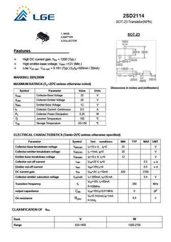
2SD2114 SOT-23 Transistor(NPN) 1. BASE SOT-23 2.EMITTER 3.COLLECTOR Features High DC current gain. hFE = 1200 (Typ.) High emitter-base voltage. VEBO =12V (Min.) Low VCE (sat). VCE (sat) = 0.18V (Typ.) (IC/IB=500mA / 20mA) MARKING BBV,BBW MAXIMUM RATINGS (TA=25 unless otherwise noted) Dimensions in inches and (millimeters) Symbol Parameter Value Units VCBO Collec... See More ⇒
8.14. Size:106K lrc
l2sd2114kvlt1g.pdf 

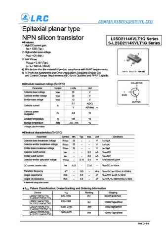
LESHAN RADIO COMPANY, LTD. Epitaxial planar type NPN silicon transistor L2SD2114KVLT1G Series Features S-L2SD2114KVLT1G Series 1) High DC current gain. hFE = 1200 (Typ.) 2) High emitter-base voltage. 3 VEBO =12V (Min.) 3) Low V CE (sat). 1 VCE (sat) = 0.18V (Typ.) 2 (IC / IB = 500mA / 20mA) 4) We declare that the material of product compliance with RoHS requirements. SOT 2... See More ⇒
8.15. Size:105K lrc
l2sd2114kwlt1g.pdf 

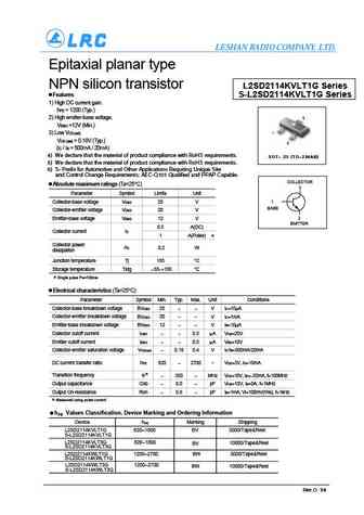
LESHAN RADIO COMPANY, LTD. Epitaxial planar type NPN silicon transistor L2SD2114KVLT1G Series Features S-L2SD2114KVLT1G Series 1) High DC current gain. hFE = 1200 (Typ.) 3 2) High emitter-base voltage. VEBO =12V (Min.) 3) Low VCE (sat). 1 VCE (sat) = 0.18V (Typ.) 2 (IC / IB = 500mA / 20mA) 4) We declare that the material of product compliance with RoHS requirements. SOT 23 (TO... See More ⇒
8.16. Size:784K kexin
2sd2114.pdf 

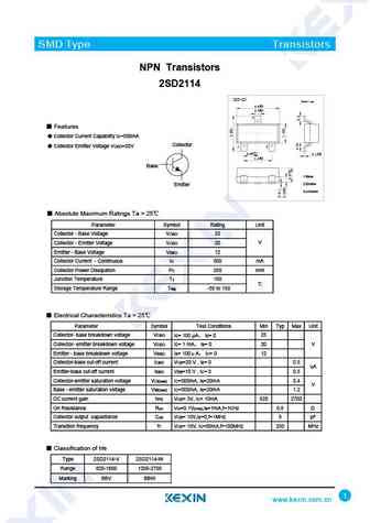
SMD Type Transistors NPN Transistors 2SD2114 SOT-23 Unit mm +0.1 2.9 -0.1 +0.1 0.4-0.1 3 Features Collector Current Capability IC=500mA Collector Collector Emitter Voltage VCEO=20V 1 2 +0.1 +0.05 0.95 -0.1 0.1 -0.01 +0.1 1.9 -0.1 Base 1.Base 2.Emitter Emitter 3.collector Absolute Maximum Ratings Ta = 25 Parameter Symbol Rating Unit Collector - Ba... See More ⇒
8.18. Size:227K inchange semiconductor
2sd2118.pdf 
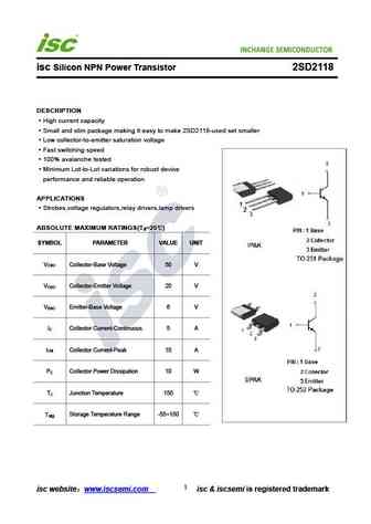
INCHANGE Semiconductor isc Silicon NPN Power Transistor 2SD2118 DESCRIPTION High current capacity Small and slim package making it easy to make 2SD2118-used set smaller Low collector-to-emitter saturation voltage Fast switching speed 100% avalanche tested Minimum Lot-to-Lot variations for robust device performance and reliable operation APPLICATIONS Strobes,voltage regu... See More ⇒
8.19. Size:197K inchange semiconductor
2sd2112.pdf 
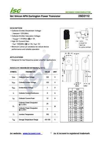
isc Silicon NPN Darlington Power Transistor 2SD2112 DESCRIPTION Collector-Emitter Breakdown Voltage- V = 120V(Min) (BR)CEO Collector-Emitter Saturation Voltage- V = 1.5V(Max) @I = 3A CE(sat) C High DC Current Gain h = 1000(Min) @ I = 3A, V = 3V FE C CE Minimum Lot-to-Lot variations for robust device performance and reliable operation APPLICATIONS Designed for low f... See More ⇒
8.20. Size:197K inchange semiconductor
2sd2113.pdf 
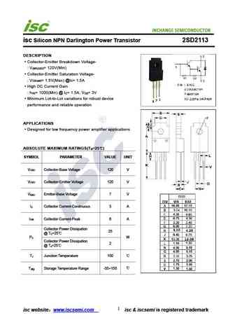
isc Silicon NPN Darlington Power Transistor 2SD2113 DESCRIPTION Collector-Emitter Breakdown Voltage- V = 120V(Min) (BR)CEO Collector-Emitter Saturation Voltage- V = 1.5V(Max) @I = 1.5A CE(sat) C High DC Current Gain h = 1000(Min) @ I = 1.5A, V = 3V FE C CE Minimum Lot-to-Lot variations for robust device performance and reliable operation APPLICATIONS Designed for l... See More ⇒
8.21. Size:197K inchange semiconductor
2sd2111.pdf 
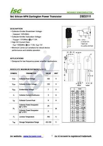
isc Silicon NPN Darlington Power Transistor 2SD2111 DESCRIPTION Collector-Emitter Breakdown Voltage- V = 120V(Min) (BR)CEO Collector-Emitter Saturation Voltage- V = 1.5V(Max) @I = 1.5A CE(sat) C High DC Current Gain h = 1000(Min) @ I = 1.5A, V = 3V FE C CE Minimum Lot-to-Lot variations for robust device performance and reliable operation APPLICATIONS Designed for l... See More ⇒
8.22. Size:193K inchange semiconductor
2sd211.pdf 
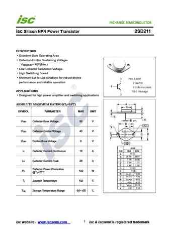
INCHANGE Semiconductor isc Silicon NPN Power Transistor 2SD211 DESCRIPTION Excellent Safe Operating Area Collector-Emitter Sustaining Voltage- V = 40V(Min.) CEO(SUS) Low Collector Saturation Voltage- High Switching Speed Minimum Lot-to-Lot variations for robust device performance and reliable operation APPLICATIONS Designed for high power amplifier and switching applic... See More ⇒
Detailed specifications: 2SD2105, 2SD2106, 2SD2107, 2SD2107B, 2SD2107C, 2SD2108, 2SD2109, 2SD211, 2SC2655, 2SD2111, 2SD2112, 2SD2113, 2SD2115, 2SD2115L, 2SD2115S, 2SD2116, 2SD2117
Keywords - 2SD2110 pdf specs
2SD2110 cross reference
2SD2110 equivalent finder
2SD2110 pdf lookup
2SD2110 substitution
2SD2110 replacement
