2SD855B Datasheet. Specs and Replacement
Type Designator: 2SD855B 📄📄
Material of Transistor: Si
Polarity: NPN
Absolute Maximum Ratings
Maximum Collector Power Dissipation (Pc): 30 W
Maximum Collector-Base Voltage |Vcb|: 100 V
Maximum Collector-Emitter Voltage |Vce|: 60 V
Maximum Emitter-Base Voltage |Veb|: 5 V
Maximum Collector Current |Ic max|: 1 A
Max. Operating Junction Temperature (Tj): 150 °C
Electrical Characteristics
Forward Current Transfer Ratio (hFE), MIN: 40
Noise Figure, dB: -
Package: TO220
- BJT ⓘ Cross-Reference Search
2SD855B datasheet
8.2. Size:212K inchange semiconductor
2sd855.pdf 
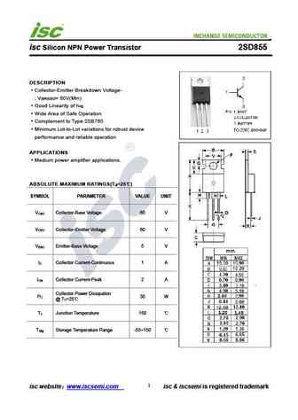
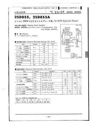
isc Silicon NPN Power Transistor 2SD855 DESCRIPTION Collector-Emitter Breakdown Voltage- V = 60V(Min) (BR)CEO Good Linearity of h FE Wide Area of Safe Operation Complement to Type 2SB760 Minimum Lot-to-Lot variations for robust device performance and reliable operation APPLICATIONS Medium power amplifier applications. ABSOLUTE MAXIMUM RATINGS(T =25 ) a SYMBOL PARA... See More ⇒
9.5. Size:189K wingshing
2sd850.pdf
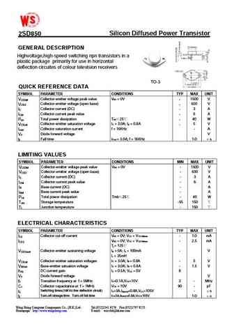
Silicon Diffused Power Transistor 2SD850 GENERAL DESCRIPTION Highvoltage,high-speed switching npn transistors in a plastic package primarily for use in horizontal deflection circuites of colour television receivers TO-3 QUICK REFERENCE DATA SYMBOL PARAMETER CONDITIONS TYP MAX UNIT Collector-emitter voltage peak value V = 0V BE V - 1500 V CESM Collector-emitter voltage (open base)... See More ⇒
9.6. Size:150K inchange semiconductor
2sd850.pdf
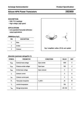
Inchange Semiconductor Product Specification Silicon NPN Power Transistors 2SD850 DESCRIPTION With TO-3 package High voltage ,high speed APPLICATIONS Line-operated horizontal deflection output applications PINNING(see fig.2) PIN DESCRIPTION 1 Base 2 Emitter Fig.1 simplified outline (TO-3) and symbol 3 Collector Absolute maximum ratings(Ta= ) SYMBOL PARAMETER... See More ⇒
9.7. Size:208K inchange semiconductor
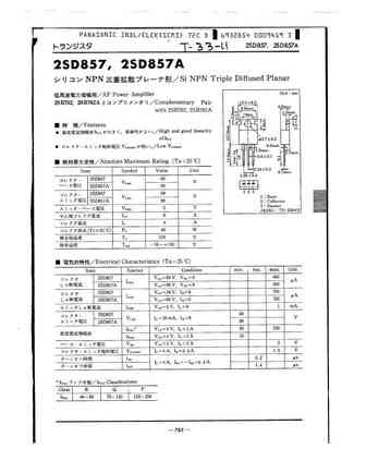
2sd857.pdf
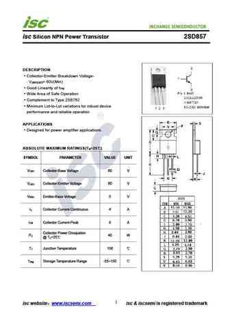
isc Silicon NPN Power Transistor 2SD857 DESCRIPTION Collector-Emitter Breakdown Voltage- V = 60V(Min) (BR)CEO Good Linearity of h FE Wide Area of Safe Operation Complement to Type 2SB762 Minimum Lot-to-Lot variations for robust device performance and reliable operation APPLICATIONS Designed for power amplifier applications. ABSOLUTE MAXIMUM RATINGS(T =25 ) a SYMBO... See More ⇒
9.8. Size:213K inchange semiconductor
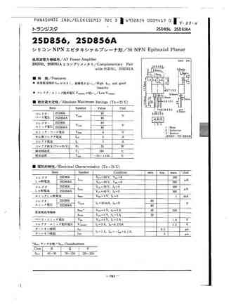
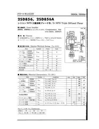
2sd856.pdf
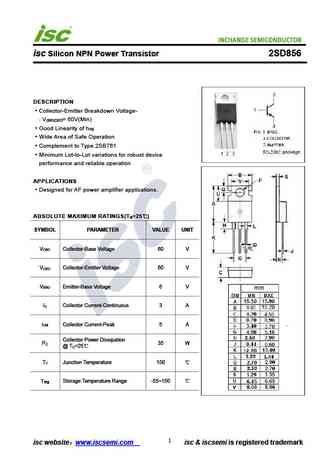
isc Silicon NPN Power Transistor 2SD856 DESCRIPTION Collector-Emitter Breakdown Voltage- V = 60V(Min) (BR)CEO Good Linearity of h FE Wide Area of Safe Operation Complement to Type 2SB761 Minimum Lot-to-Lot variations for robust device performance and reliable operation APPLICATIONS Designed for AF power amplifier applications. ABSOLUTE MAXIMUM RATINGS(T =25 ) a SY... See More ⇒
9.9. Size:212K inchange semiconductor
2sd859.pdf
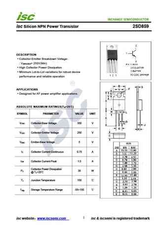
isc Silicon NPN Power Transistor 2SD859 DESCRIPTION Collector-Emitter Breakdown Voltage- V = 250V(Min) (BR)CEO High Collector Power Dissipation Minimum Lot-to-Lot variations for robust device performance and reliable operation APPLICATIONS Designed for AF power amplifier applications. ABSOLUTE MAXIMUM RATINGS(T =25 ) a SYMBOL PARAMETER VALUE UNIT V Collector-Base Voltag... See More ⇒
9.10. Size:217K inchange semiconductor
2sd858.pdf
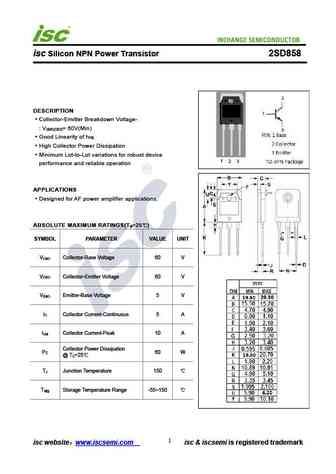
isc Silicon NPN Power Transistor 2SD858 DESCRIPTION Collector-Emitter Breakdown Voltage- V = 60V(Min) (BR)CEO Good Linearity of h FE High Collector Power Dissipation Minimum Lot-to-Lot variations for robust device performance and reliable operation APPLICATIONS Designed for AF power amplifier applications. ABSOLUTE MAXIMUM RATINGS(T =25 ) a SYMBOL PARAMETER VALUE UNI... See More ⇒
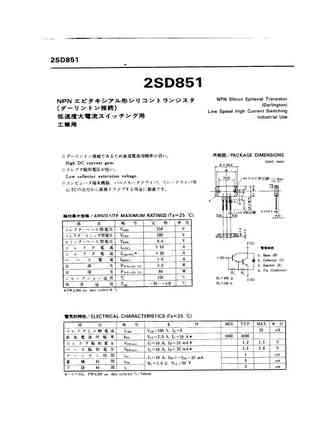
Detailed specifications: 2SD848A, 2SD849, 2SD850, 2SD851, 2SD852, 2SD854, 2SD855, 2SD855A, 2SC2625, 2SD856, 2SD856A, 2SD856B, 2SD857, 2SD857A, 2SD857B, 2SD858, 2SD858A
Keywords - 2SD855B pdf specs
2SD855B cross reference
2SD855B equivalent finder
2SD855B pdf lookup
2SD855B substitution
2SD855B replacement