BCW31LT3 Specs and Replacement
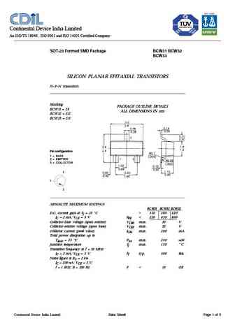
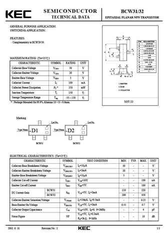
Type Designator: BCW31LT3
Material of Transistor: Si
Polarity: NPN
Absolute Maximum Ratings
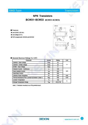
Maximum Collector Power Dissipation (Pc): 0.3 W
Maximum Collector-Base Voltage |Vcb|: 30 V
Maximum Collector-Emitter Voltage |Vce|: 20 V
Maximum Emitter-Base Voltage |Veb|: 5 V
Maximum Collector Current |Ic max|: 0.1 A
Max. Operating Junction Temperature (Tj): 150 °C
Electrical Characteristics
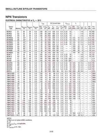
Transition Frequency (ft): 300 MHz
Collector Capacitance (Cc): 4 pF
Forward Current Transfer Ratio (hFE), MIN: 110
Package: TO236
BCW31LT3 Substitution
- BJT ⓘ Cross-Reference Search
BCW31LT3 datasheet
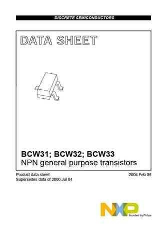
DISCRETE SEMICONDUCTORS DATA SHEET BCW31; BCW32; BCW33 NPN general purpose transistors Product data sheet 2004 Feb 06 Supersedes data of 2000 Jul 04 NXP Semiconductors Product data sheet BCW31; BCW32; NPN general purpose transistors BCW33 FEATURES PINNING Low current (100 mA) PIN DESCRIPTION Low voltage (32 V). 1 base 2 emitter APPLICATIONS 3 collector General ... See More ⇒
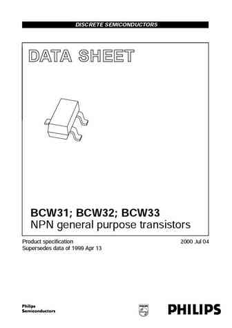
DISCRETE SEMICONDUCTORS DATA SHEET ok, halfpage M3D088 BCW31; BCW32; BCW33 NPN general purpose transistors Product specification 2000 Jul 04 Supersedes data of 1999 Apr 13 Philips Semiconductors Product specification NPN general purpose transistors BCW31; BCW32; BCW33 FEATURES PINNING Low current (100 mA) PIN DESCRIPTION Low voltage (32 V). 1 base 2 emitter APPLICATIONS... See More ⇒
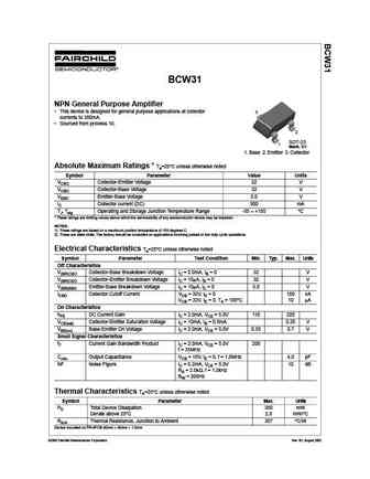
BCW31 NPN General Purpose Amplifier This device is designed for general purpose applications at collector 3 currents to 300mA. Sourced from process 10. 2 SOT-23 1 Mark D1 1. Base 2. Emitter 3. Collector Absolute Maximum Ratings * Ta=25 C unless otherwise noted Symbol Parameter Value Units VCEO Collector-Emitter Voltage 32 V VCBO Collector-Base Voltage 32 V VEBO Emitte... See More ⇒
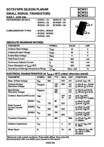
Important notice Dear Customer, On 7 February 2017 the former NXP Standard Product business became a new company with the tradename Nexperia. Nexperia is an industry leading supplier of Discrete, Logic and PowerMOS semiconductors with its focus on the automotive, industrial, computing, consumer and wearable application markets In data sheets and application notes which still contain... See More ⇒
Detailed specifications: BCW30, BCW30CSM, BCW30LT1, BCW30LT3, BCW30R, BCW31, BCW31CSM, BCW31LT1, 9014, BCW31R, BCW32, BCW32CSM, BCW32LT1, BCW32LT3, BCW32R, BCW33, BCW33CSM
Keywords - BCW31LT3 pdf specs
BCW31LT3 cross reference
BCW31LT3 equivalent finder
BCW31LT3 pdf lookup
BCW31LT3 substitution
BCW31LT3 replacement
