BDW51A Datasheet. Specs and Replacement
Type Designator: BDW51A
Material of Transistor: Si
Polarity: NPN
Absolute Maximum Ratings
Maximum Collector Power Dissipation (Pc): 117 W
Maximum Collector-Base Voltage |Vcb|: 60 V
Maximum Collector-Emitter Voltage |Vce|: 60 V
Maximum Emitter-Base Voltage |Veb|: 5 V
Maximum Collector Current |Ic max|: 15 A
Max. Operating Junction Temperature (Tj): 200 °C
Electrical Characteristics
Transition Frequency (ft): 3 MHz
Forward Current Transfer Ratio (hFE), MIN: 20
Package: TO3
BDW51A Substitution
- BJT ⓘ Cross-Reference Search
BDW51A datasheet
bdw51 bdw51a bdw51b bdw51c.pdf ![]()
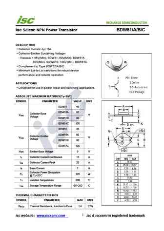
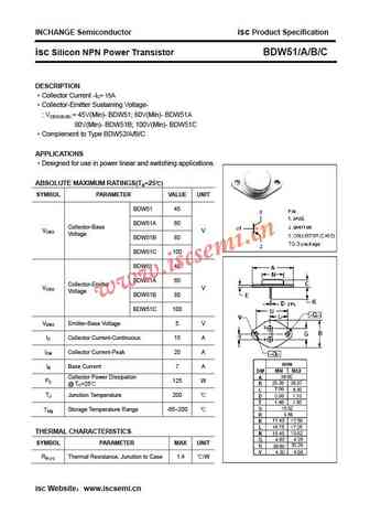
isc Silicon NPN Power Transistor BDW51/A/B/C DESCRIPTION Collector Current -I = 15A C Collector-Emitter Sustaining Voltage- V = 45V(Min)- BDW51; 60V(Min)- BDW51A CEO(SUS) 80V(Min)- BDW51B; 100V(Min)- BDW51C Complement to Type BDW52/A/B/C Minimum Lot-to-Lot variations for robust device performance and reliable operation APPLICATIONS Designed for use in power linear and sw... See More ⇒
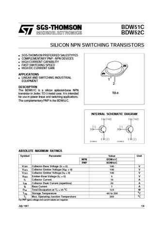
BDW51C BDW52C SILICON NPN SWITCHING TRANSISTORS SGS-THOMSON PREFERRED SALESTYPES COMPLEMENTARY PNP - NPN DEVICES HIGH CURRENT CAPABILITY FAST SWITCHING SPEED HIGH DC CURRENT GAIN APPLICATIONS LINEAR AND SWITCHING INDUSTRIAL 1 EQUIPMENT 2 DESCRIPTION The BDW51C is a silicon epitaxial-base NPN TO-3 transistor in Jedec TO-3 metal case. It is intended for use in power ... See More ⇒
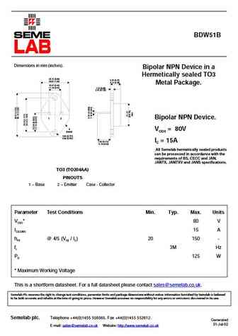
BDW51B Dimensions in mm (inches). Bipolar NPN Device in a Hermetically sealed TO3 25.15 (0.99) 6.35 (0.25) 26.67 (1.05) 9.15 (0.36) Metal Package. 10.67 (0.42) 11.18 (0.44) 1.52 (0.06) 3.43 (0.135) 1 2 Bipolar NPN Device. 3 VCEO = 80V (case) 3.84 (0.151) 4.09 (0.161) 7.92 (0.312) IC = 15A 12.70 (0.50) All Semelab hermetically sealed products can be processed in a... See More ⇒
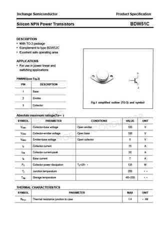
Inchange Semiconductor Product Specification Silicon NPN Power Transistors BDW51C DESCRIPTION With TO-3 package Complement to type BDW52C Excellent safe operating area APPLICATIONS For use in power linear and switching applications PINNING(see Fig.2) PIN DESCRIPTION 1 Base 2 Emitter Fig.1 simplified outline (TO-3) and symbol 3 Collector Absolute maximum ratings... See More ⇒
Detailed specifications: BDW41, BDW42, BDW43, BDW44, BDW45, BDW46, BDW48, BDW51, A1015, BDW51B, BDW51C, BDW52, BDW52A, BDW52C, BDW53, BDW53A, BDW53B
Keywords - BDW51A pdf specs
BDW51A cross reference
BDW51A equivalent finder
BDW51A pdf lookup
BDW51A substitution
BDW51A replacement
