C442 Specs and Replacement
Type Designator: C442
Material of Transistor: Si
Polarity: NPN
Absolute Maximum Ratings
Maximum Collector Power Dissipation (Pc): 0.38 W
Maximum Collector-Base Voltage |Vcb|: 40 V
Maximum Collector-Emitter Voltage |Vce|: 30 V
Maximum Emitter-Base Voltage |Veb|: 10 V
Max. Operating Junction Temperature (Tj): 175 °C
Electrical Characteristics
Transition Frequency (ft): 130 MHz
Collector Capacitance (Cc): 14 pF
Forward Current Transfer Ratio (hFE), MIN: 115
Noise Figure, dB: -
Package: TO18
- BJT ⓘ Cross-Reference Search
C442 datasheet
0.1. Size:71K 1
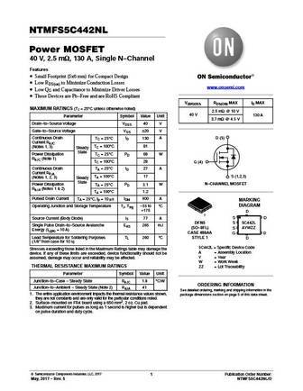
ntmfs5c442nlt1g.pdf 

NTMFS5C442NL Power MOSFET 40 V, 2.5 mW, 130 A, Single N-Channel Features Small Footprint (5x6 mm) for Compact Design Low RDS(on) to Minimize Conduction Losses www.onsemi.com Low QG and Capacitance to Minimize Driver Losses These Devices are Pb-Free and are RoHS Compliant V(BR)DSS RDS(ON) MAX ID MAX MAXIMUM RATINGS (TJ = 25 C unless otherwise noted) 2.5 mW @ 10 V 40 ... See More ⇒
0.2. Size:121K 1
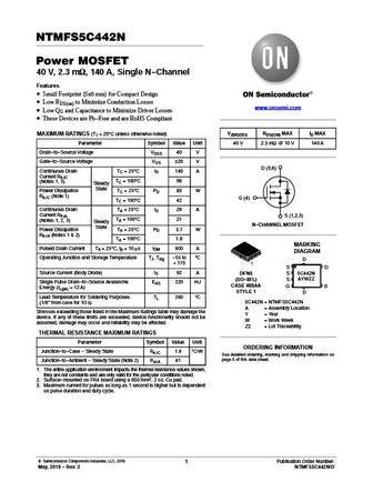
ntmfs5c442nt3g.pdf 

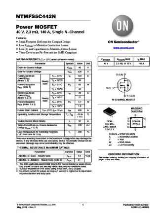
NTMFS5C442N Power MOSFET 40 V, 2.3 mW, 140 A, Single N-Channel Features Small Footprint (5x6 mm) for Compact Design Low RDS(on) to Minimize Conduction Losses www.onsemi.com Low QG and Capacitance to Minimize Driver Losses These Devices are Pb-Free and are RoHS Compliant V(BR)DSS RDS(ON) MAX ID MAX MAXIMUM RATINGS (TJ = 25 C unless otherwise noted) Parameter Symbol Va... See More ⇒
0.3. Size:106K sanyo
2sc4428.pdf 

Ordering number EN2851 NPN Triple Diffused Planar Silicon Transistor 2SC4428 800V/6A Switching Regulator Applications Features Package Dimensions High breakdown voltage, high reliability. unit mm Fast switching speed (tf 0.1 s typ). 2039D Wide ASO. [2SC4428] Adoption of MBIT process. 16.0 5.6 3.4 Micaless package facilitating easy mounting. 3.1 2.8 2.0 2... See More ⇒
0.4. Size:107K sanyo
2sc4429.pdf 

Ordering number EN2852 NPN Triple Diffused Planar Silicon Transistor 2SC4429 800V/8A Switching Regulator Applications Features Package Dimensions High breakdown voltage, high reliability. unit mm Fast switching speed (tf 0.1 s typ). 2039D Wide ASO. [2SC4429] Adoption of MBIT process. 16.0 5.6 3.4 Micaless package facilitating easy mounting. 3.1 2.8 2.0 2... See More ⇒
0.5. Size:101K sanyo
2sc4425.pdf 

Ordering number EN2848 NPN Triple Diffused Planar Silicon Transistor 2SC4425 400V/25A Switching Regulator Applications Features Package Dimensions High breakdown voltage, high reliability. unit mm Fast switching speed (tf 0.1 s typ). 2039D Wide ASO. [2SC4425] Adoption of MBIT process. 16.0 5.6 3.4 Micaless package facilitating easy mounting. 3.1 2.8 2.0 ... See More ⇒
0.6. Size:105K sanyo
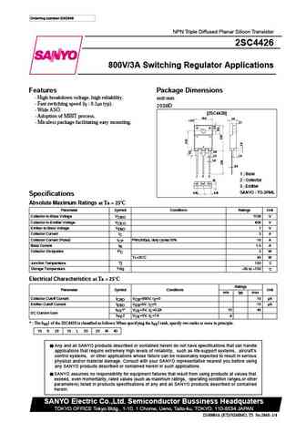
2sc4426.pdf 

Ordering number EN2849 NPN Triple Diffused Planar Silicon Transistor 2SC4426 800V/3A Switching Regulator Applications Features Package Dimensions High breakdown voltage, high reliability. unit mm Fast switching speed (tf 0.1 s typ). 2039D Wide ASO. [2SC4426] Adoption of MBIT process. 16.0 5.6 3.4 Micaless package facilitating easy mounting. 3.1 2.8 2.0 2... See More ⇒
0.7. Size:104K sanyo
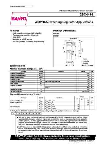
2sc4424.pdf 

Ordering number EN2847 NPN Triple Diffused Planar Silicon Transistor 2SC4424 400V/16A Switching Regulator Applications Features Package Dimensions High breakdown voltage, high reliability. unit mm Fast switching speed (tf 0.1 s typ). 2039D Wide ASO. [2SC4424] Adoption of MBIT process. 16.0 5.6 3.4 Micaless package facilitating easy mounting. 3.1 2.8 2.0 ... See More ⇒
0.8. Size:102K sanyo
2sc4423.pdf 

Ordering number EN2854 NPN Triple Diffused Planar Silicon Transistor 2SC4423 400V/12A Switching Regulator Applications Features Package Dimensions High breakdown voltage, high reliability. unit mm Fast switching speed (tf 0.1 s typ). 2039D Wide ASO. [2SC4423] Adoption of MBIT process. 16.0 5.6 3.4 Micaless package facilitating easy mounting. 3.1 2.8 2.0 ... See More ⇒
0.9. Size:108K sanyo
2sc4427.pdf 

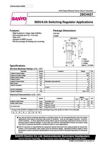
Ordering number EN2850 NPN Triple Diffused Planar Silicon Transistor 2SC4427 800V/4.5A Switching Regulator Applications Features Package Dimensions High breakdown voltage, high reliability. unit mm Fast switching speed (tf 0.1 s typ). 2039D Wide ASO. [2SC4427] Adoption of MBIT process. 16.0 5.6 3.4 Micaless package facilitating easy mounting. 3.1 2.8 2.0... See More ⇒
0.10. Size:121K onsemi
ntmfs5c442n.pdf 

NTMFS5C442N Power MOSFET 40 V, 2.3 mW, 140 A, Single N-Channel Features Small Footprint (5x6 mm) for Compact Design Low RDS(on) to Minimize Conduction Losses www.onsemi.com Low QG and Capacitance to Minimize Driver Losses These Devices are Pb-Free and are RoHS Compliant V(BR)DSS RDS(ON) MAX ID MAX MAXIMUM RATINGS (TJ = 25 C unless otherwise noted) Parameter Symbol Va... See More ⇒
0.11. Size:72K onsemi
ntmfs5c442nl.pdf 

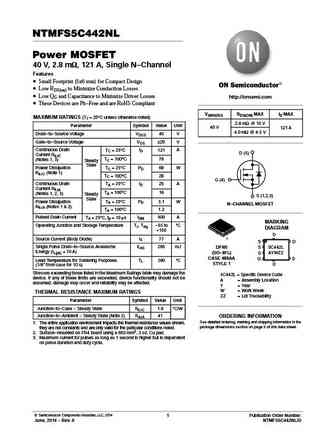
NTMFS5C442NL Power MOSFET 40 V, 2.8 mW, 121 A, Single N-Channel Features Small Footprint (5x6 mm) for Compact Design Low RDS(on) to Minimize Conduction Losses Low QG and Capacitance to Minimize Driver Losses http //onsemi.com These Devices are Pb-Free and are RoHS Compliant V(BR)DSS RDS(ON) MAX ID MAX MAXIMUM RATINGS (TJ = 25 C unless otherwise noted) 2.8 mW @ 10 V ... See More ⇒
0.12. Size:181K onsemi
nvmfs5c442n.pdf 

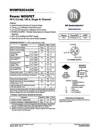
NVMFS5C442N Power MOSFET 40 V, 2.3 mW, 140 A, Single N-Channel Features Small Footprint (5x6 mm) for Compact Design Low RDS(on) to Minimize Conduction Losses www.onsemi.com Low QG and Capacitance to Minimize Driver Losses NVMFS5C442NWF - Wettable Flank Option for Enhanced Optical Inspection V(BR)DSS RDS(ON) MAX ID MAX AEC-Q101 Qualified and PPAP Capable 40 V 2.3 ... See More ⇒
0.13. Size:73K onsemi
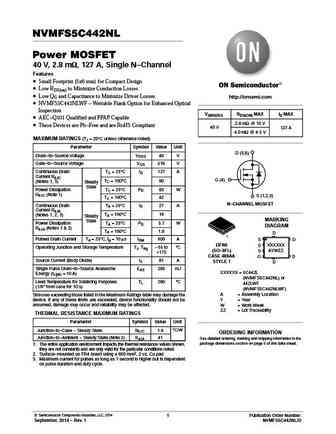
nvmfs5c442nl.pdf 

NVMFS5C442NL Power MOSFET 40 V, 2.8 mW, 127 A, Single N-Channel Features Small Footprint (5x6 mm) for Compact Design Low RDS(on) to Minimize Conduction Losses Low QG and Capacitance to Minimize Driver Losses http //onsemi.com NVMFS5C442NLWF - Wettable Flank Option for Enhanced Optical Inspection V(BR)DSS RDS(ON) MAX ID MAX AEC-Q101 Qualified and PPAP Capable 2.8 ... See More ⇒
0.14. Size:115K onsemi
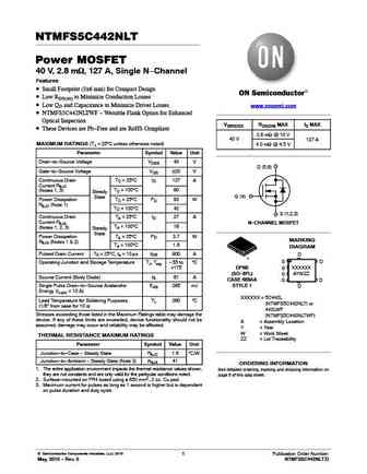
ntmfs5c442nlt.pdf 

NTMFS5C442NLT Power MOSFET 40 V, 2.8 mW, 127 A, Single N-Channel Features Small Footprint (5x6 mm) for Compact Design Low RDS(on) to Minimize Conduction Losses Low QG and Capacitance to Minimize Driver Losses www.onsemi.com NTMFS5C442NLTWF - Wettable Flank Option for Enhanced Optical Inspection V(BR)DSS RDS(ON) MAX ID MAX These Devices are Pb-Free and are RoHS Com... See More ⇒
0.15. Size:82K panasonic
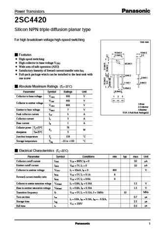
2sc4420.pdf 

Power Transistors 2SC4420 Silicon NPN triple diffusion planar type For high breakdown voltage high-speed switching Unit mm 15.0 0.3 5.0 0.2 Features 11.0 0.2 3.2 High-speed switching High collector to base voltage VCBO 3.2 0.1 Wide area of safe operation (ASO) Satisfactory linearity of foward current transfer ratio hFE Full-pack package which can be installed to the hea... See More ⇒
0.16. Size:48K hitachi
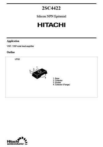
2sc4422.pdf 

2SC4422 Silicon NPN Epitaxial Application VHF / UHF wide band amplifier Outline UPAK 1 2 3 4 1. Base 2. Collector 3. Emitter 4. Collector (Flange) 2SC4422 Absolute Maximum Ratings (Ta = 25 C) Item Symbol Ratings Unit Collector to base voltage VCBO 15 V Collector to emitter voltage VCEO 11 V Emitter to base voltage VEBO 2V Collector current IC 50 mA Collector power dissipa... See More ⇒
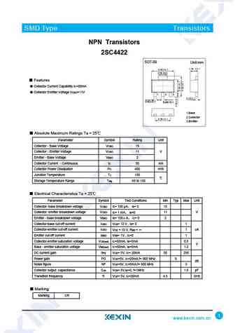
0.18. Size:998K kexin
2sc4422.pdf 

SMD Type Transistors NPN Transistors 2SC4422 SOT-89 Unit mm 1.70 0.1 Features Collector Current Capability IC=50mA Collector Emitter Voltage VCEO=11V 0.42 0.1 0.46 0.1 1.Base 2.Collector 3.Emitter Absolute Maximum Ratings Ta = 25 Parameter Symbol Rating Unit Collector - Base Voltage VCBO 15 Collector - Emitter Voltage VCEO 11 V Emitter - Base Voltage VE... See More ⇒
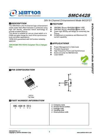
0.19. Size:378K semtron
smc4428.pdf 

SMC4428 30V N-Channel Enhancement Mode MOSFET DESCRIPTION FEATURE The SMC4428 is the N-Channel logic enhancement 30V/20A, RDS(ON) =6m (typ.)@VGS =10V mode power field effect transistor is produced using 30V/16A, RDS(ON) =8m (typ.)@VGS =4.5V high cell density. advanced trench technology to Super high density cell design for extremely low provide excellent R... See More ⇒
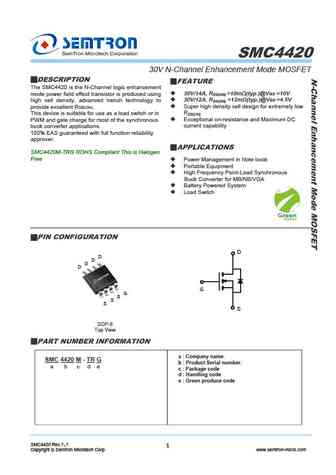
0.20. Size:380K semtron
smc4420.pdf 

SMC4420 30V N-Channel Enhancement Mode MOSFET DESCRIPTION FEATURE The SMC4420 is the N-Channel logic enhancement 30V/14A, RDS(ON) =10m (typ.)@VGS =10V mode power field effect transistor is produced using 30V/12A, RDS(ON) =12m (typ.)@VGS =4.5V high cell density. advanced trench technology to Super high density cell design for extremely low provide excellent... See More ⇒
0.21. Size:195K inchange semiconductor
2sc4428.pdf 
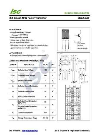
INCHANGE Semiconductor isc Silicon NPN Power Transistor 2SC4428 DESCRIPTION High Breakdown Voltage- V = 800V(Min) (BR)CEO Fast Switching speed Wide Area of Safe Operation 100% avalanche tested Minimum Lot-to-Lot variations for robust device performance and reliable operation APPLICATIONS Designed for switching regulator Applications ABSOLUTE MAXIMUM RATINGS(Ta=25 ) ... See More ⇒
0.22. Size:225K inchange semiconductor
2sc4429.pdf 
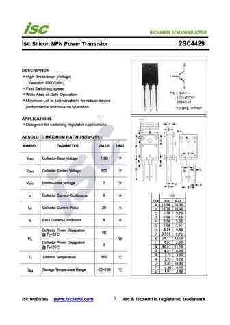
isc Silicon NPN Power Transistor 2SC4429 DESCRIPTION High Breakdown Voltage- V = 800V(Min) (BR)CEO Fast Switching speed Wide Area of Safe Operation Minimum Lot-to-Lot variations for robust device performance and reliable operation APPLICATIONS Designed for switching regulator Applications ABSOLUTE MAXIMUM RATINGS(Ta=25 ) SYMBOL PARAMETER VALUE UNIT V Collector-Base Vo... See More ⇒
0.23. Size:184K inchange semiconductor
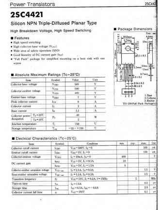
2sc4421.pdf 
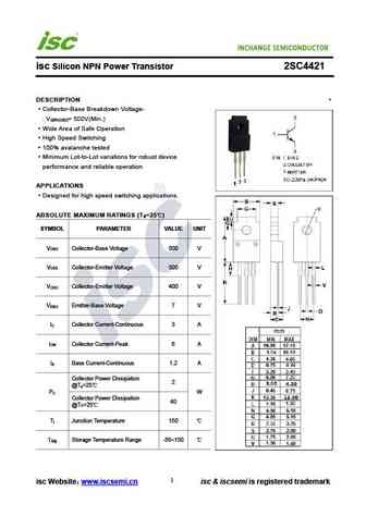
INCHANGE Semiconductor isc Silicon NPN Power Transistor 2SC4421 DESCRIPTION Collector-Base Breakdown Voltage- V = 500V(Min.) (BR)CBO Wide Area of Safe Operation High Speed Switching 100% avalanche tested Minimum Lot-to-Lot variations for robust device performance and reliable operation APPLICATIONS Designed for high speed switching applications. ABSOLUTE MAXIMUM RA... See More ⇒
0.24. Size:195K inchange semiconductor
2sc4425.pdf 
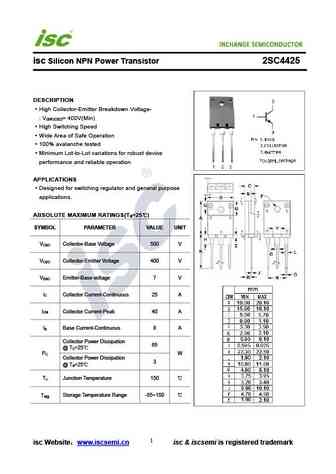
INCHANGE Semiconductor isc Silicon NPN Power Transistor 2SC4425 DESCRIPTION High Collector-Emitter Breakdown Voltage- V = 400V(Min) (BR)CEO High Switching Speed Wide Area of Safe Operation 100% avalanche tested Minimum Lot-to-Lot variations for robust device performance and reliable operation APPLICATIONS Designed for switching regulator and general purpose applicatio... See More ⇒
0.25. Size:195K inchange semiconductor
2sc4426.pdf 
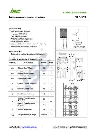
INCHANGE Semiconductor isc Silicon NPN Power Transistor 2SC4426 DESCRIPTION High Breakdown Voltage- V = 800V(Min) (BR)CEO Fast Switching speed Wide Area of Safe Operation 100% avalanche tested Minimum Lot-to-Lot variations for robust device performance and reliable operation APPLICATIONS Designed for switching regulator Applications ABSOLUTE MAXIMUM RATINGS(Ta=25 ) ... See More ⇒
0.26. Size:221K inchange semiconductor
2sc4424.pdf 
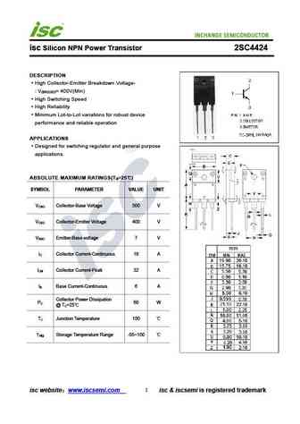
isc Silicon NPN Power Transistor 2SC4424 DESCRIPTION High Collector-Emitter Breakdown Voltage- V = 400V(Min) (BR)CEO High Switching Speed High Reliability Minimum Lot-to-Lot variations for robust device performance and reliable operation APPLICATIONS Designed for switching regulator and general purpose applications. ABSOLUTE MAXIMUM RATINGS(T =25 ) a SYMBOL PARAMETER... See More ⇒
0.27. Size:221K inchange semiconductor
2sc4423.pdf 
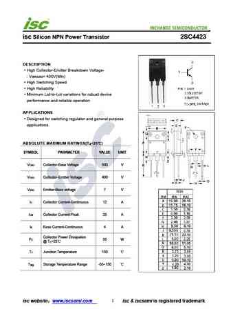
isc Silicon NPN Power Transistor 2SC4423 DESCRIPTION High Collector-Emitter Breakdown Voltage- V = 400V(Min) (BR)CEO High Switching Speed High Reliability Minimum Lot-to-Lot variations for robust device performance and reliable operation APPLICATIONS Designed for switching regulator and general purpose applications. ABSOLUTE MAXIMUM RATINGS(T =25 ) a SYMBOL PARAMETER... See More ⇒
0.28. Size:196K inchange semiconductor
2sc4427.pdf 
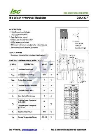
INCHANGE Semiconductor isc Silicon NPN Power Transistor 2SC4427 DESCRIPTION High Breakdown Voltage- V = 800V(Min) (BR)CEO Fast Switching speed Wide Area of Safe Operation 100% avalanche tested Minimum Lot-to-Lot variations for robust device performance and reliable operation APPLICATIONS Designed for switching regulator Applications ABSOLUTE MAXIMUM RATINGS(Ta=25 ) ... See More ⇒
Detailed specifications: C407, C420, C424, C425, C426, C428, C434, C441, 2N3904, C450, C5, C50-28, C5-8, C5-8Z, C5T2192, C5T2432, C5T2484
Keywords - C442 pdf specs
C442 cross reference
C442 equivalent finder
C442 pdf lookup
C442 substitution
C442 replacement
