2N3443 Specs and Replacement
Type Designator: 2N3443
Material of Transistor: Ge
Polarity: PNP
Absolute Maximum Ratings
Maximum Collector Power Dissipation (Pc): 0.3 W
Maximum Collector-Base Voltage |Vcb|: 20 V
Maximum Collector-Emitter Voltage |Vce|: 15 V
Maximum Collector Current |Ic max|: 0.1 A
Max. Operating Junction Temperature (Tj): 100 °C
Electrical Characteristics
Transition Frequency (ft): 75 MHz
Collector Capacitance (Cc): 2.5 pF
Forward Current Transfer Ratio (hFE), MIN: 20
Noise Figure, dB: -
Package: TO5
- BJT ⓘ Cross-Reference Search
2N3443 datasheet
9.1. Size:135K motorola
2n3442r7.pdf 

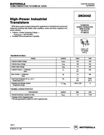
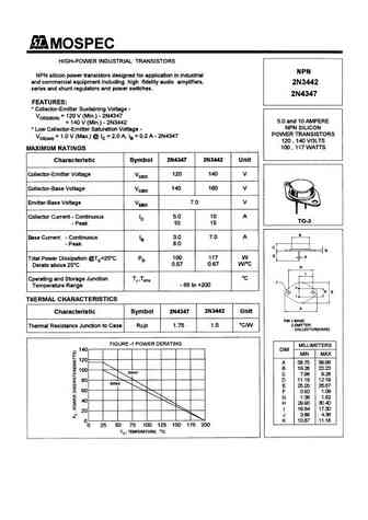
Order this document MOTOROLA by 2N3442/D SEMICONDUCTOR TECHNICAL DATA 2N3442 High-Power Industrial Transistors 10 AMPERE NPN silicon power transistor designed for applications in industrial and commercial POWER TRANSISTOR equipment including high fidelity audio amplifiers, series and shunt regulators and NPN SILICON power switches. 140 VOLTS Collector Emitter Sustaining Vol... See More ⇒
9.2. Size:47K st
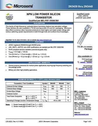
2n3439 2n3440.pdf 

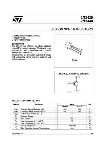
2N3439 2N3440 SILICON NPN TRANSISTORS STMicroelectronics PREFERRED SALESTYPES NPN TRANSISTOR DESCRIPTION The 2N3439 and 2N3440 are silicon epitaxial planar NPN transistors in jedec TO-39 metal case designed for use in consumer and industrial line-operated applications. These devices are particularly suited as drivers in high-voltage low current inverters, switching and seri... See More ⇒
9.3. Size:61K central
2n3442.pdf 

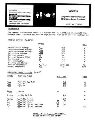
145 Adams Avenue, Hauppauge, NY 11788 USA Tel (631) 435-1110 Fax (631) 435-1824 ... See More ⇒
9.4. Size:65K onsemi
2n3442g.pdf 

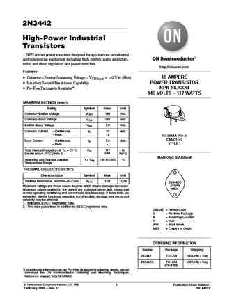
2N3442 High-Power Industrial Transistors NPN silicon power transistor designed for applications in industrial and commercial equipment including high fidelity audio amplifiers, series and shunt regulators and power switches. http //onsemi.com Features 10 AMPERE Collector -Emitter Sustaining Voltage - VCEO(sus) = 140 Vdc (Min) POWER TRANSISTOR Excellent Second Breakdown Capabi... See More ⇒
9.5. Size:65K onsemi
2n3442-d.pdf 

2N3442 High-Power Industrial Transistors NPN silicon power transistor designed for applications in industrial and commercial equipment including high fidelity audio amplifiers, series and shunt regulators and power switches. http //onsemi.com Features 10 AMPERE Collector -Emitter Sustaining Voltage - VCEO(sus) = 140 Vdc (Min) POWER TRANSISTOR Excellent Second Breakdown Capabi... See More ⇒
9.6. Size:197K comset
2n3442-2n4347.pdf 

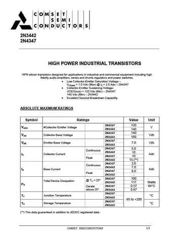
2N3442 2N4347 HIGH POWER INDUSTRIAL TRANSISTORS HIGH POWER INDUSTRIAL TRANSISTORS NPN silicon transistors designed for applications in industrial and commercial equipment including high fidelity audio amplifiers, series and shunts regulators and power switches. Low Collector-Emitter Saturation Voltage VCE(sat) = 1.0 Vdc (Max) @ IC = 2.0 Adc 2N4347 Collector-Emitter Susta... See More ⇒
9.8. Size:94K semelab
2n3440c3c.pdf 

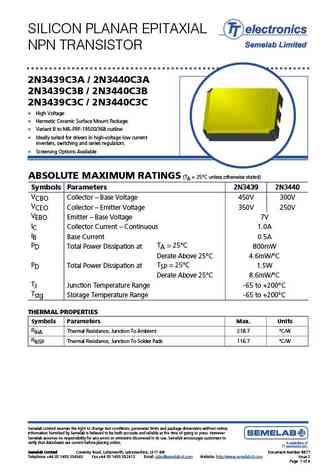
SILICON PLANAR EPITAXIAL NPN TRANSISTOR 2N3439C3A / 2N3440C3A 2N3439C3B / 2N3440C3B 2N3439C3C / 2N3440C3C High Voltage Hermetic Ceramic Surface Mount Package. Variant B to MIL-PRF-19500/368 outline Ideally suited for drivers in high-voltage low current inverters, switching and series regulators. Screening Options Available ABSOLUTE MAXIMUM RATINGS (TA =... See More ⇒
9.9. Size:94K semelab
2n3440c3a.pdf 

SILICON PLANAR EPITAXIAL NPN TRANSISTOR 2N3439C3A / 2N3440C3A 2N3439C3B / 2N3440C3B 2N3439C3C / 2N3440C3C High Voltage Hermetic Ceramic Surface Mount Package. Variant B to MIL-PRF-19500/368 outline Ideally suited for drivers in high-voltage low current inverters, switching and series regulators. Screening Options Available ABSOLUTE MAXIMUM RATINGS (TA =... See More ⇒
9.10. Size:13K semelab
2n3441.pdf 

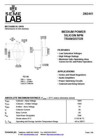
2N3441 SEME LAB MECHANICAL DATA Dimensions in mm (inches) MEDIUM POWER SILICON NPN 6.35 (0.250) 8.64 (0.340) 3.68 (0.145) rad. TRANSISTOR 3.61 (0.142) max. 3.86 (0.145) rad. FEATURES Low Saturation Voltages High Voltage Ratings Maximum Safe Operating Area Curves for DC and Pulse Operation. 1.27 (0.050) 1.91 (0.750) 4.83 (0.190) 5.33 (0.210) 9.14 (0.360)... See More ⇒
9.11. Size:94K semelab
2n3440c3b.pdf 

SILICON PLANAR EPITAXIAL NPN TRANSISTOR 2N3439C3A / 2N3440C3A 2N3439C3B / 2N3440C3B 2N3439C3C / 2N3440C3C High Voltage Hermetic Ceramic Surface Mount Package. Variant B to MIL-PRF-19500/368 outline Ideally suited for drivers in high-voltage low current inverters, switching and series regulators. Screening Options Available ABSOLUTE MAXIMUM RATINGS (TA =... See More ⇒
9.12. Size:94K semelab
2n3440csm4r.pdf 

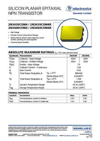
SILICON PLANAR EPITAXIAL NPN TRANSISTOR 2N3439CSM4 / 2N3439CSM4R 2N3440CSM4 / 2N3440CSM4R High Voltage Hermetic Ceramic Surface Mount Package. Ideally suited for drivers in high-voltage low current inverters, switching and series regulators. Screening Options Available ABSOLUTE MAXIMUM RATINGS (TA = 25 C unless otherwise stated) 2N3439 2N3440 Symbols Parame... See More ⇒
9.13. Size:11K semelab
2n3447.pdf 

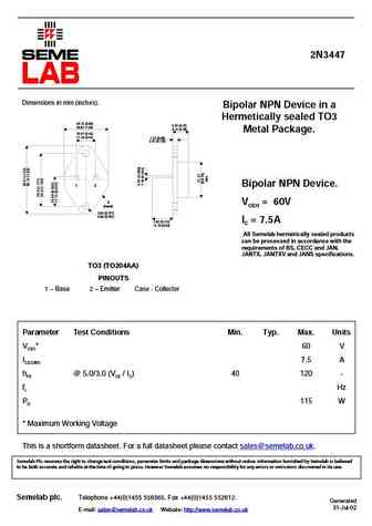
2N3447 Dimensions in mm (inches). Bipolar NPN Device in a Hermetically sealed TO3 25.15 (0.99) 6.35 (0.25) 26.67 (1.05) 9.15 (0.36) Metal Package. 10.67 (0.42) 11.18 (0.44) 1.52 (0.06) 3.43 (0.135) 1 2 Bipolar NPN Device. 3 VCEO = 60V (case) 3.84 (0.151) 4.09 (0.161) 7.92 (0.312) IC = 7.5A 12.70 (0.50) All Semelab hermetically sealed products can be processed in ... See More ⇒
9.14. Size:11K semelab
2n3445.pdf 

2N3445 Dimensions in mm (inches). Bipolar NPN Device in a Hermetically sealed TO3 25.15 (0.99) 6.35 (0.25) 26.67 (1.05) 9.15 (0.36) Metal Package. 10.67 (0.42) 11.18 (0.44) 1.52 (0.06) 3.43 (0.135) 1 2 Bipolar NPN Device. 3 VCEO = 60V (case) 3.84 (0.151) 4.09 (0.161) 7.92 (0.312) IC = 7.5A 12.70 (0.50) All Semelab hermetically sealed products can be processed in ... See More ⇒
9.15. Size:21K semelab
2n3440dcsm.pdf 

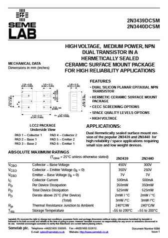
2N3439DCSM 2N3440DCSM HIGH VOLTAGE, MEDIUM POWER, NPN DUAL TRANSISTOR IN A HERMETICALLY SEALED MECHANICAL DATA CERAMIC SURFACE MOUNT PACKAGE Dimensions in mm (inches) FOR HIGH RELIABILITY APPLICATIONS FEATURES 2.29 0.20 1.65 0.13 1.40 0.15 (0.055 0.006) (0.09 0.008) (0.065 0.005) DUAL SILICON PLANAR EPITAXIAL NPN TRANSISTOR 2 3 HERMETIC CERAMIC SURFACE... See More ⇒
9.16. Size:172K jmnic
2n3445.pdf 

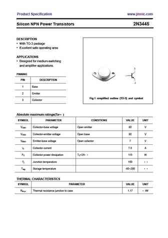
Product Specification www.jmnic.com Silicon NPN Power Transistors 2N3445 DESCRIPTION With TO-3 package Excellent safe operating area APPLICATIONS Designed for medium-switching and amplifier applications. PINNING PIN DESCRIPTION 1 Base 2 Emitter Fig.1 simplified outline (TO-3) and symbol 3 Collector Absolute maximum ratings(Ta= ) SYMBOL PARAMETER CONDITIONS VALU... See More ⇒
9.17. Size:172K jmnic
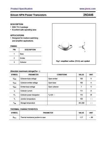
2n3446.pdf 

Product Specification www.jmnic.com Silicon NPN Power Transistors 2N3446 DESCRIPTION With TO-3 package Excellent safe operating area APPLICATIONS Designed for medium-switching and amplifier applications. PINNING PIN DESCRIPTION 1 Base 2 Emitter Fig.1 simplified outline (TO-3) and symbol 3 Collector Absolute maximum ratings(Ta= ) SYMBOL PARAMETER CONDITIONS VALU... See More ⇒
9.18. Size:272K microsemi
2n3439 2n3440.pdf 

2N3439 thru 2N3440 Qualified Levels NPN LOW POWER SILICON JAN, JANTX, Available on TRANSISTOR JANTXV and JANS commercial versions Qualified per MIL-PRF-19500/368 DESCRIPTION This family of high-frequency, epitaxial planar transistors feature low saturation voltage. These devices are also available in TO-39 and low profile U4 and UA packaging. Microsemi also offers nume... See More ⇒
9.19. Size:190K microsemi
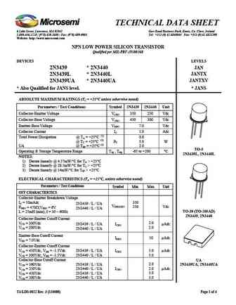
2n3440ua.pdf 

TECHNICAL DATA SHEET 6 Lake Street, Lawrence, MA 01841 Gort Road Business Park, Ennis, Co. Clare, Ireland 1-800-446-1158 / (978) 620-2600 / Fax (978) 689-0803 Tel +353 (0) 65 6840044 Fax +353 (0) 65 6822298 Website http //www.microsemi.com NPN LOW POWER SILICON TRANSISTOR Qualified per MIL-PRF-19500/368 DEVICES LEVELS JAN 2N3439 * 2N3440 JANTX 2N3439L * 2N3440L JANTXV ... See More ⇒
9.20. Size:129K inchange semiconductor
2n3448.pdf 
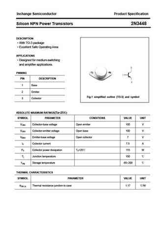
Inchange Semiconductor Product Specification Silicon NPN Power Transistors 2N3448 DESCRIPTION With TO-3 package Excellent Safe Operating Area APPLICATIONS Designed for medium-switching and amplifier applications. PINNING PIN DESCRIPTION 1 Base 2 Emitter Fig.1 simplified outline (TO-3) and symbol 3 Collector ABSOLUTE MAXIMUM RATINGS(Ta=25 ) SYMBOL PARAMETER CON... See More ⇒
9.21. Size:130K inchange semiconductor
2n3441.pdf 
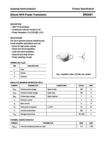
Inchange Semiconductor Product Specification Silicon NPN Power Transistors 2N3441 DESCRIPTION With TO-66 package Continuous collector current-IC=3A Power dissipation -PD=25W @TC=25 APPLICATIONS For use in general-purpose switching and Linear amplifier applications such as Driver for high power outputs Series and shunt regulators Audio and servo amplifiers ... See More ⇒
9.23. Size:130K inchange semiconductor
2n3442.pdf 
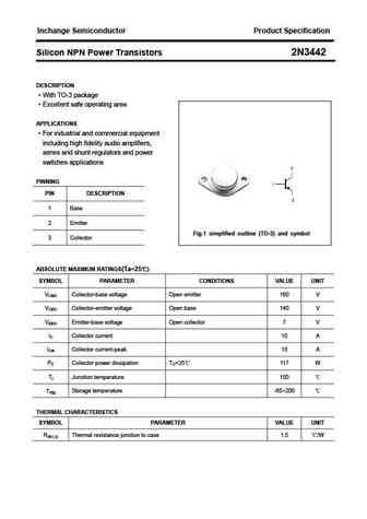
Inchange Semiconductor Product Specification Silicon NPN Power Transistors 2N3442 DESCRIPTION With TO-3 package Excellent safe operating area APPLICATIONS For industrial and commercial equipment including high fidelity audio amplifiers, series and shunt regulators and power switches applications PINNING PIN DESCRIPTION 1 Base 2 Emitter Fig.1 simplified outline (T... See More ⇒
9.24. Size:129K inchange semiconductor
2n3447.pdf 
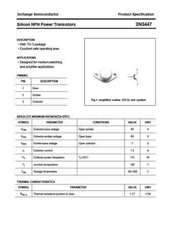
Inchange Semiconductor Product Specification Silicon NPN Power Transistors 2N3447 DESCRIPTION With TO-3 package Excellent safe operating area APPLICATIONS Designed for medium-switching and amplifier applications. PINNING PIN DESCRIPTION 1 Base 2 Emitter Fig.1 simplified outline (TO-3) and symbol 3 Collector ABSOLUTE MAXIMUM RATINGS(Ta=25 ) SYMBOL PARAMETER CON... See More ⇒
9.25. Size:114K inchange semiconductor
2n3445.pdf 
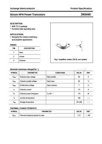
Inchange Semiconductor Product Specification Silicon NPN Power Transistors 2N3445 DESCRIPTION With TO-3 package Excellent safe operating area APPLICATIONS Designed for medium-switching and amplifier applications. PINNING PIN DESCRIPTION 1 Base 2 Emitter Fig.1 simplified outline (TO-3) and symbol 3 Collector Absolute maximum ratings(Ta= ) SYMBOL PARAMETER CONDI... See More ⇒
9.26. Size:114K inchange semiconductor
2n3446.pdf 
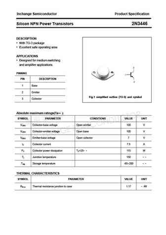
Inchange Semiconductor Product Specification Silicon NPN Power Transistors 2N3446 DESCRIPTION With TO-3 package Excellent safe operating area APPLICATIONS Designed for medium-switching and amplifier applications. PINNING PIN DESCRIPTION 1 Base 2 Emitter Fig.1 simplified outline (TO-3) and symbol 3 Collector Absolute maximum ratings(Ta= ) SYMBOL PARAMETER CONDI... See More ⇒
Detailed specifications: 2N3440
, 2N3440CSM4
, 2N3440L
, 2N3440S
, 2N3441
, 2N3441X
, 2N3441Y
, 2N3442
, 13007
, 2N3444
, 2N3444S
, 2N3445
, 2N3446
, 2N3447
, 2N3448
, 2N3449
, 2N345
.
History: 2N3446
Keywords - 2N3443 pdf specs
2N3443 cross reference
2N3443 equivalent finder
2N3443 pdf lookup
2N3443 substitution
2N3443 replacement
