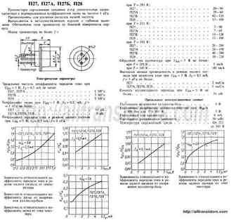
P28 Specs and Replacement
Type Designator: P28
Material of Transistor: Ge
Polarity: PNP
Absolute Maximum Ratings
Maximum Collector Power Dissipation (Pc): 0.03 W
Maximum Collector-Base Voltage |Vcb|: 5 V
Maximum Collector Current |Ic max|: 0.006 A
Max. Operating Junction Temperature (Tj): 75 °C
Electrical Characteristics
Transition Frequency (ft): 5 MHz
Collector Capacitance (Cc): 50 pF
Forward Current Transfer Ratio (hFE), MIN: 20
Noise Figure, dB: -
P28 Substitution
- BJT ⓘ Cross-Reference Search
P28 datasheet
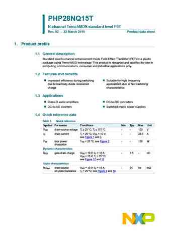
PHP28NQ15T N-channel TrenchMOS standard level FET Rev. 02 22 March 2010 Product data sheet 1. Product profile 1.1 General description Standard level N-channel enhancement mode Field-Effect Transistor (FET) in a plastic package using TrenchMOS technology. This product is designed and qualified for use in computing, communications, consumer and industrial applications only. 1.2 Feat... See More ⇒
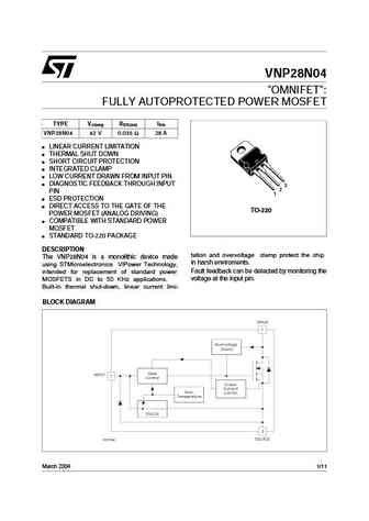
VNP28N04 "OMNIFET" FULLY AUTOPROTECTED POWER MOSFET TYPE V R I clamp DS(on) lim VNP28N04 42 V 0.035 28 A LINEAR CURRENT LIMITATION THERMAL SHUT DOWN SHORT CIRCUIT PROTECTION INTEGRATED CLAMP LOW CURRENT DRAWN FROM INPUT PIN DIAGNOSTIC FEEDBACK THROUGH INPUT 3 2 PIN 1 ESD PROTECTION DIRECT ACCESS TO THE GATE OF THE TO-220 POWER MOSFET (ANALOG DRIVING) COMPATIBLE... See More ⇒
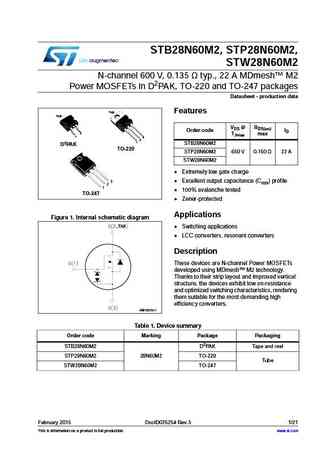
stb28n60m2 sti28n60m2 stp28n60m2 stw28n60m2.pdf ![]()
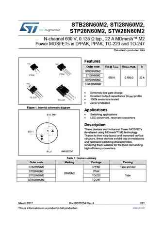
STB28N60M2, STI28N60M2, STP28N60M2, STW28N60M2 N-channel 600 V, 0.135 typ., 22 A MDmesh M2 Power MOSFETs in D PAK, I PAK, TO-220 and TO-247 Datasheet - production data Features Order code V @ T R max. I DS Jmax DS(on) D STB28N60M2 STI28N60M2 650 V 0.150 22 A STP28N60M2 STW28N60M2 Extremely low gate charge Excellent output capacitance (C ) profile ... See More ⇒
stb28n65m2 stf28n65m2 stp28n65m2 stw28n65m2.pdf ![]()
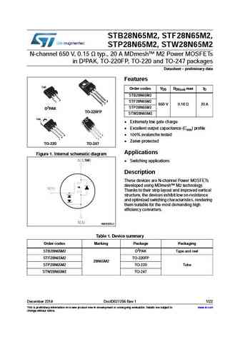
STB28N65M2, STF28N65M2, STP28N65M2, STW28N65M2 N-channel 650 V, 0.15 typ., 20 A MDmesh M2 Power MOSFETs in D PAK, TO-220FP, TO-220 and TO-247 packages Datasheet - preliminary data Features TAB Order codes VDS RDS(on) max ID STB28N65M2 3 3 STF28N65M2 1 2 650 V 0.18 20 A 1 STP28N65M2 D2PAK TO-220FP STW28N65M2 TAB Extremely low gate charge Excellent output... See More ⇒
stb28nm50n stf28nm50n stp28nm50n stw28nm50n.pdf ![]()
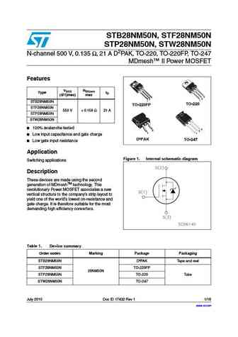
STB28NM50N, STF28NM50N STP28NM50N, STW28NM50N N-channel 500 V, 0.135 , 21 A D2PAK, TO-220, TO-220FP, TO-247 MDmesh II Power MOSFET Features VDSS RDS(on) Type ID (@Tjmax) max 3 3 2 2 1 1 STB28NM50N TO-220 TO-220FP STF28NM50N 550 V ... See More ⇒
stb28nm60nd stf28nm60nd stp28nm60nd stw28nm60nd.pdf ![]()
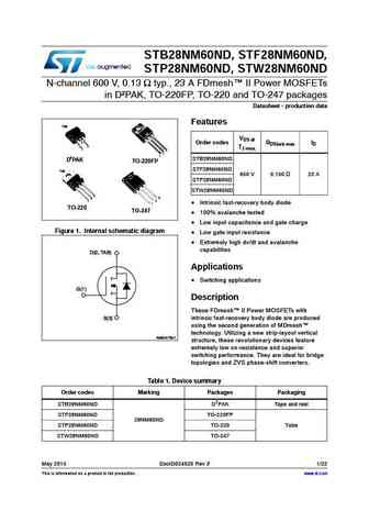
STB28NM60ND, STF28NM60ND, STP28NM60ND, STW28NM60ND N-channel 600 V, 0.13 typ., 23 A FDmesh II Power MOSFETs in D PAK, TO-220FP, TO-220 and TO-247 packages Datasheet - production data Features TAB VDS @ 2 Order codes RDS(on) max ID 3 TJ max. 1 3 2 1 2 STB28NM60ND D PAK TO-220FP STF28NM60ND TAB 650 V 0.150 23 A STP28NM60ND STW28NM60ND 3 3 3 2 2 1 2 1 1... See More ⇒
stb28n60m2 stp28n60m2 stw28n60m2.pdf ![]()
STB28N60M2, STP28N60M2, STW28N60M2 N-channel 600 V, 0.135 typ., 22 A MDmesh M2 Power MOSFETs in D2PAK, TO-220 and TO-247 packages Datasheet - production data TAB Features TAB VDS @ RDS(on) Order code ID 3 TJmax max 1 3 2 1 STB28N60M2 D2PAK TO-220 STP28N60M2 650 V 0.150 22 A STW28N60M2 Extremely low gate charge 3 Excellent output capacitance (Coss) prof... See More ⇒
vnp28n04fi vnb28n04 vnv28n04.pdf ![]()
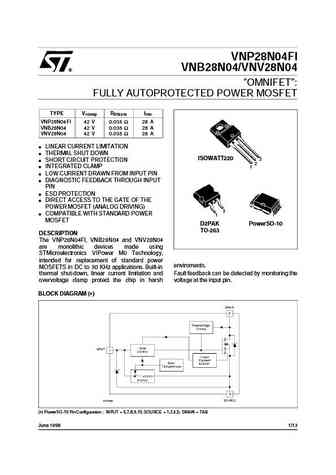
VNP28N04FI VNB28N04/VNV28N04 OMNIFET FULLY AUTOPROTECTED POWER MOSFET TYPE V R I clamp DS(on) lim VNP28N04FI 42 V 0.035 28 A VNB28N04 42 V 0.035 28 A VNV28N04 42 V 0.035 28 A LINEAR CURRENT LIMITATION THERMAL SHUT DOWN ISOWATT220 3 SHORT CIRCUIT PROTECTION 2 INTEGRATED CLAMP 1 LOW CURRENT DRAWN FROM INPUT PIN DIAGNOSTIC FEEDBACK THROUGH INPUT PI... See More ⇒

VNP28N04 "OMNIFET" FULLY AUTOPROTECTED POWER MOSFET TYPE V R I clamp DS(on) lim VNP28N04 42 V 0.035 28 A LINEAR CURRENT LIMITATION THERMAL SHUT DOWN SHORT CIRCUIT PROTECTION INTEGRATED CLAMP LOW CURRENT DRAWN FROM INPUT PIN DIAGNOSTIC FEEDBACK THROUGH INPUT 3 2 PIN 1 ESD PROTECTION DIRECT ACCESS TO THE GATE OF THE TO-220 POWER MOSFET (ANALOG DRIVING) COMPATIBLE... See More ⇒
stb28n60dm2 stp28n60dm2 stw28n60dm2.pdf ![]()
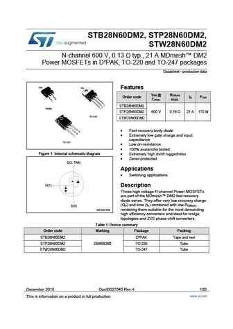
STB28N60DM2, STP28N60DM2, STW28N60DM2 N-channel 600 V, 0.13 typ., 21 A MDmesh DM2 Power MOSFETs in D PAK, TO-220 and TO-247 packages Datasheet - production data Features V @ R DS DS(on) Order code I P D TOT T max. Jmax. STB28N60DM2 STP28N60DM2 600 V 0.16 21 A 170 W STW28N60DM2 Fast-recovery body diode Extremely low gate charge and input capacita... See More ⇒
SSM6P28TU TOSHIBA Field-Effect Transistor Silicon P-Channel MOS Type SSM6P28TU High-Speed Switching Applications Power Management Switch Applications Unit mm 1.8V drive 2.1 0.1 P-ch 2-in-1 1.7 0.1 Low ON-resistance Ron = 460 m (max) (@VGS = -1.8 V) Ron = 306 m (max) (@VGS = -2.5 V) 1 6 Ron = 234 m (max) (@VGS = -4.0 V) 5 2 Absolute Maximum Rati... See More ⇒
Preliminary Data Sheet R07DS0507EJ0100 NP28N10SDE Rev.1.00 Sep 16, 2011 MOS FIELD EFFECT TRANSISTOR Description The NP28N10SDE is N-channel MOS Field Effect Transistor designed for high current switching applications. Features Low on-state resistance RDS(on)1 = 52 m MAX. (VGS = 10 V, ID = 14 A) RDS(on)2 = 59 m MAX. (VGS = 4.5 V, ID = 14 A) Low Ciss Ciss = 2200... See More ⇒
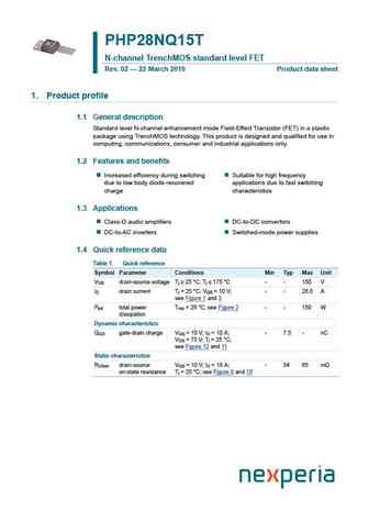
PHP28NQ15T N-channel TrenchMOS standard level FET Rev. 02 22 March 2010 Product data sheet 1. Product profile 1.1 General description Standard level N-channel enhancement mode Field-Effect Transistor (FET) in a plastic package using TrenchMOS technology. This product is designed and qualified for use in computing, communications, consumer and industrial applications only. 1.2 Feat... See More ⇒
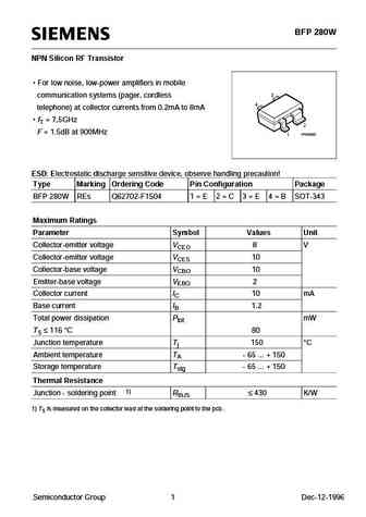
BFP 280W NPN Silicon RF Transistor For low noise, low-power amplifiers in mobile communication systems (pager, cordless telephone) at collector currents from 0.2mA to 8mA fT = 7,5GHz F = 1.5dB at 900MHz ESD Electrostatic discharge sensitive device, observe handling precaution! Type Marking Ordering Code Pin Configuration Package BFP 280W REs Q62702-F1504 1 = E 2 = C 3 = E 4... See More ⇒
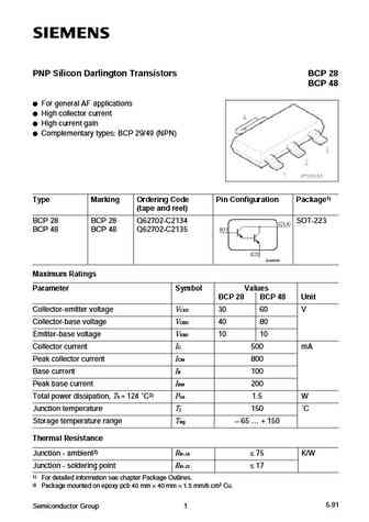
PNP Silicon Darlington Transistors BCP 28 BCP 48 For general AF applications High collector current High current gain Complementary types BCP 29/49 (NPN) Type Marking Ordering Code Pin Configuration Package1) (tape and reel) BCP 28 BCP 28 Q62702-C2134 SOT-223 BCP 48 BCP 48 Q62702-C2135 Maximum Ratings Parameter Symbol Values BCP 28 BCP 48 Unit Collector-emitter voltage VCE0 3... See More ⇒
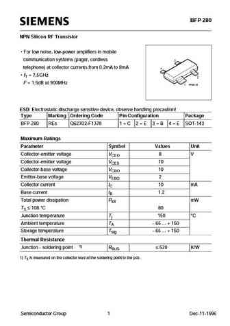
BFP 280 NPN Silicon RF Transistor For low noise, low-power amplifiers in mobile communication systems (pager, cordless telephone) at collector currents from 0.2mA to 8mA fT = 7,5GHz F = 1.5dB at 900MHz ESD Electrostatic discharge sensitive device, observe handling precaution! Type Marking Ordering Code Pin Configuration Package BFP 280 REs Q62702-F1378 1 = C 2 = E 3 = B 4 =... See More ⇒
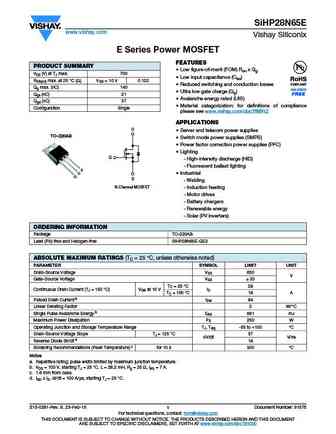
SUP28N15-52 Vishay Siliconix N-Channel 150-V (D-S) 175 C MOSFET FEATURES PRODUCT SUMMARY TrenchFET Power MOSFET VDS (V) RDS(on) ( )ID (A) 175 C Junction Temperature 0.052 at VGS = 10 V 28 150 PWM Optimized 0.060 at VGS = 6 V 26 Compliant to RoHS Directive 2002/95/EC APPLICATIONS Primary Side Switch TO-220AB D G DRAIN connected to TAB G D S... See More ⇒
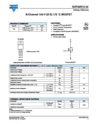
SiHP28N60EF www.vishay.com Vishay Siliconix EF Series Power MOSFET with Fast Body Diode FEATURES PRODUCT SUMMARY Fast body diode MOSFET using E series VDS (V) at TJ max. 650 technology Reduced trr, Qrr, and IRRM RDS(on) max. at 25 C ( ) VGS = 10 V 0.123 Low figure-of-merit (FOM) Ron x Qg Qg (Max.) (nC) 120 Low input capacitance (Ciss) Qgs (nC) 17 Low switc... See More ⇒

SUP28N15-52 Vishay Siliconix N-Channel 150-V (D-S) 175 C MOSFET FEATURES PRODUCT SUMMARY TrenchFET Power MOSFET VDS (V) RDS(on) ( )ID (A) 175 C Junction Temperature 0.052 at VGS = 10 V 28 150 PWM Optimized 0.060 at VGS = 6 V 26 Compliant to RoHS Directive 2002/95/EC APPLICATIONS Primary Side Switch TO-220AB D G DRAIN connected to TAB G D S... See More ⇒
IKP28N65ES5 High speed switching series 5 th generation TRENCHSTOPTM 5 high speed soft switching IGBT copacked with full rated current RAPID 1 fast and soft anti parallel diode C Features and Benefits High speed S5 technology offering High speed smooth switching device for hard & soft switching Very Low V CEsat 650V breakdown voltage G Low Q G E IGBT copacked... See More ⇒
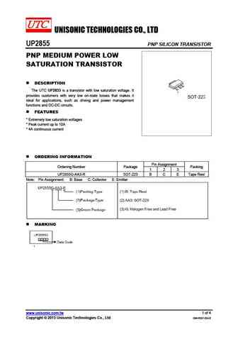
UNISONIC TECHNOLOGIES CO., LTD UP2855 PNP SILICON TRANSISTOR PNP MEDIUM POWER LOW SATURATION TRANSISTOR DESCRIPTION The UTC UP2855 is a transistor with low saturation voltage. It provides customers with very low on-state losses that makes it ideal for applications, such as driving and power management functions and DC-DC circuits. FEATURES * Extremely low saturation ... See More ⇒
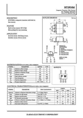
RT2P28M Composite Transistor With Resistor For Switching Application Silicon PNP Epitaxial Type OUTLINE DRAWING Unit mm DESCRIPTION 2.1 RT2P28M is composite transistor with built-in 1.25 bias resistor. FEATURE Built-in bias resistor (R2=47k ) Mini package for easy mounting APPLICATION Inverted circuit, Switching circuit, Interface circui... See More ⇒
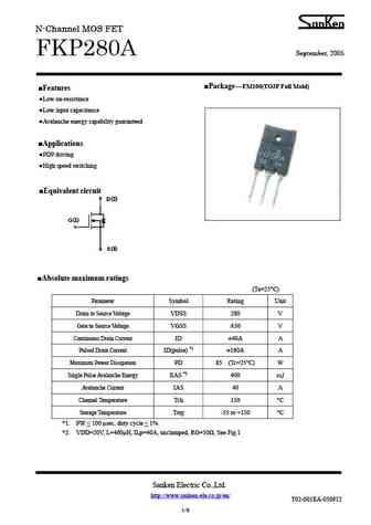
N-Channel MOS FET FKP280A September, 2005 Package---FM100(TO3P Full Mold) Features Low on-resistance Low input capacitance Avalanche energy capability guaranteed Applications PDP driving High speed switching Equivalent circuit (2) (1) (3) Absolute maximum ratings (Ta=25 C) Parameter Symbol Rating Unit Drain to Source Vol... See More ⇒
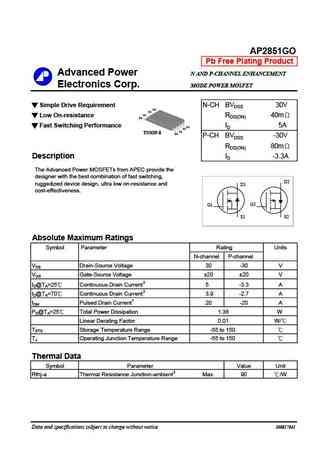
AP2851GO Pb Free Plating Product Advanced Power N AND P-CHANNEL ENHANCEMENT Electronics Corp. MODE POWER MOSFET Simple Drive Requirement N-CH BVDSS 30V G2 S2 S2 Low On-resistance RDS(ON) 40m D2 Fast Switching Performance G1 ID 5A S1 S1 TSSOP-8 D1 P-CH BVDSS -30V RDS(ON) 80m Description ID -3.3A The Advanced Power ... See More ⇒
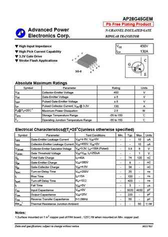
AP28G45GEM Pb Free Plating Product Advanced Power N-CHANNEL INSULATED GATE Electronics Corp. BIPOLAR TRANSISTOR High Input Impedance VCE 450V High Pick Current Capability ICP 130A C C 3.3V Gate Drive C C Strobe Flash Applications C G G E E SO-8 E E Absolute Maximum Ratings Symbol Parameter Rating ... See More ⇒
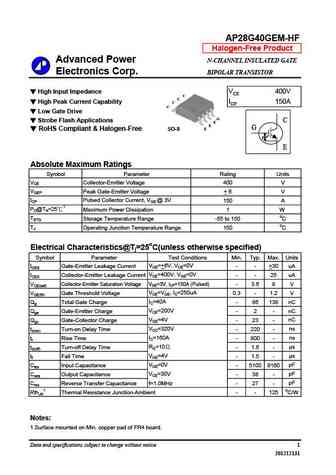
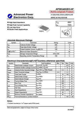
AP28G40GEM-HF Halogen-Free Product Advanced Power N-CHANNEL INSULATED GATE Electronics Corp. BIPOLAR TRANSISTOR High Input Impedance VCE 400V C C High Peak Current Capability C ICP 150A C Low Gate Drive G Strobe Flash Applications C E E G E RoHS Compliant & Halogen-Free SO-8 E Absolute Maximum Ratings Symbol Parameter Rating Units VCE Collector-Emitter V... See More ⇒
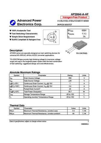
AP2864I-A-HF Halogen-Free Product Advanced Power N-CHANNEL ENHANCEMENT MODE Electronics Corp. POWER MOSFET 100% Avalanche Test BVDSS 650V D Fast Switching Characteristic RDS(ON) 1.1 Simple Drive Requirement ID 7A G RoHS Compliant & Halogen-Free S Description G D AP2864 series are specially designed as main switching devices for S TO-220CFM(I) universal 90 265VA... See More ⇒
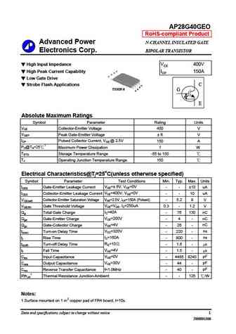
AP28G40GEO RoHS-compliant Product Advanced Power N-CHANNEL INSULATED GATE Electronics Corp. BIPOLAR TRANSISTOR High Input Impedance VCE 400V C High Peak Current Capability ICP 150A C C C Low Gate Drive Strobe Flash Applications C G E E TSSOP-8 G E E Absolute Maximum Ratings Symbol Parameter Rating Units VCE Collector-Emitter Voltage 400 V VGEP Peak Gate-E... See More ⇒
AP28G45GEO-HF RoHS-compliant Product Advanced Power N-CHANNEL INSULATED GATE Electronics Corp. BIPOLAR TRANSISTOR High Input Impedance VCE 400V High Peak Current Capability E ICP 150A E E G Low Gate Drive Strobe Flash Applications C C C C TSSOP-8 G C E Absolute Maximum Ratings Symbol Parameter Rating Units VCE Collector-Emitter Voltage 400 V VGE Peak Gate-... See More ⇒

AP2852GO Pb Free Plating Product Advanced Power N AND P-CHANNEL ENHANCEMENT Electronics Corp. MODE POWER MOSFET Simple Drive Requirement N-CH BVDSS 30V G2 S2 S2 Low On-resistance RDS(ON) 32m D2 Fast Switching Perfromance G1 ID 5.5A S1 S1 TSSOP-8 D1 P-CH BVDSS -30V RDS(ON) 50m Description ID -4.4A The Advanced Powe... See More ⇒
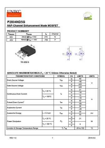
P2804ND5G N&P-Channel Enhancement Mode MOSFET PRODUCT SUMMARY V(BR)DSS RDS(ON) ID Channel 28m @VGS =10V 40V 21A N 48m @VGS = -10V -40V -16A P TO-252-5 ABSOLUTE MAXIMUM RATINGS (TA = 25 C Unless Otherwise Noted) PARAMETERS/TEST CONDITIONS SYMBOL CH. LIMITS UNITS N 40 VDS Drain-Source Voltage P -40 V N 20 VGS Gate-Source Voltage P 20 N 21 TC = 25 C P -16 ID ... See More ⇒
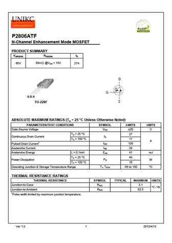
P2806ATF N-Channel Enhancement Mode MOSFET PRODUCT SUMMARY V(BR)DSS RDS(ON) ID 60V 30m @VGS = 10V 27A TO-220F ABSOLUTE MAXIMUM RATINGS (TA = 25 C Unless Otherwise Noted) PARAMETERS/TEST CONDITIONS SYMBOL LIMITS UNITS VGS Gate-Source Voltage 20 V TC = 25 C 27 ID Continuous Drain Current TC = 100 C 17 A IDM 105 Pulsed Drain Current1 IAS Avalanche Current 29 E... See More ⇒
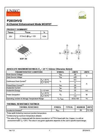
P2803HVG N-Channel Enhancement Mode MOSFET PRODUCT SUMMARY V(BR)DSS RDS(ON) ID 30V 27.5m @VGS = 10V 6.5A SOP- 08 ABSOLUTE MAXIMUM RATINGS (TA = 25 C Unless Otherwise Noted) PARAMETERS/TEST CONDITIONS SYMBOL LIMITS UNITS VDS Drain-Source Voltage 30 V VGS Gate-Source Voltage 20 TA = 25 C 6.5 ID Continuous Drain Current2 TA = 70 C 5 A IDM 30 Pulsed Drain Curre... See More ⇒
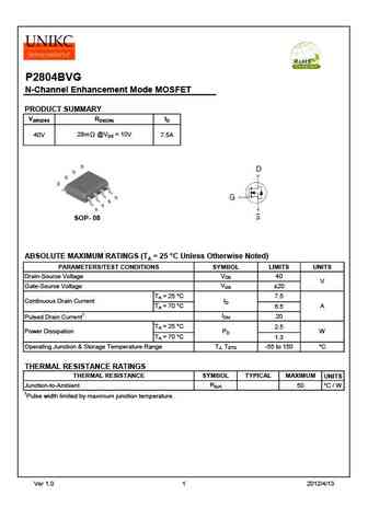
P2804BVG N-Channel Enhancement Mode MOSFET PRODUCT SUMMARY V(BR)DSS RDS(ON) ID 40V 28m @VGS = 10V 7.5A SOP- 08 ABSOLUTE MAXIMUM RATINGS (TA = 25 C Unless Otherwise Noted) PARAMETERS/TEST CONDITIONS SYMBOL LIMITS UNITS VDS Drain-Source Voltage 40 V VGS Gate-Source Voltage 20 TA = 25 C 7.5 ID Continuous Drain Current TA = 70 A C 6.5 IDM 20 Pulsed Drain Current... See More ⇒
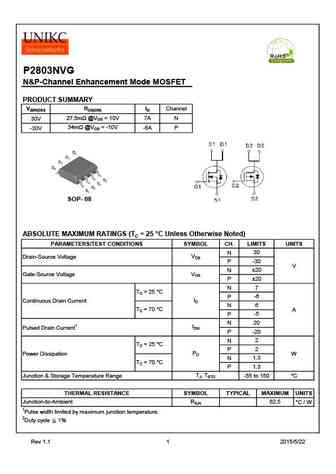
P2803NVG N&P-Channel Enhancement Mode MOSFET PRODUCT SUMMARY V(BR)DSS RDS(ON) ID Channel 27.5m @VGS = 10V 30V 7A N 34m @VGS = -10V -30V -6A P SOP- 08 ABSOLUTE MAXIMUM RATINGS (TC = 25 C Unless Otherwise Noted) PARAMETERS/TEST CONDITIONS SYMBOL CH. LIMITS UNITS N 30 VDS Drain-Source Voltage P -30 V N 20 VGS Gate-Source Voltage P 20 N 7 TC = 25 C P -6 ID Co... See More ⇒
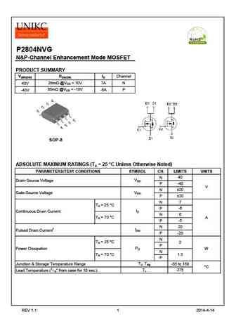
P2804NVG N&P-Channel Enhancement Mode MOSFET PRODUCT SUMMARY V(BR)DSS RDS(ON) ID Channel 28m @VGS = 10V 40V 7A N 65m @VGS = -10V -40V -6A P SOP-8 ABSOLUTE MAXIMUM RATINGS (TA = 25 C Unless Otherwise Noted) PARAMETERS/TEST CONDITIONS SYMBOL CH. LIMITS UNITS N 40 VDS Drain-Source Voltage P -40 V N 20 VGS Gate-Source Voltage P 20 N 7 TA = 25 C P -6 ID Contin... See More ⇒
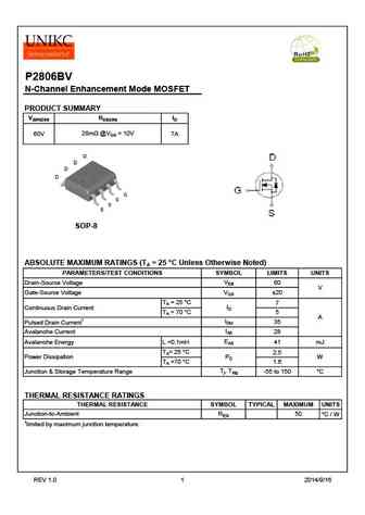
P2806BV N-Channel Enhancement Mode MOSFET PRODUCT SUMMARY V(BR)DSS RDS(ON) ID 28m @VGS = 10V 60V 7A SOP-8 ABSOLUTE MAXIMUM RATINGS (TA = 25 C Unless Otherwise Noted) PARAMETERS/TEST CONDITIONS SYMBOL LIMITS UNITS Drain-Source Voltage VDS 60 V VGS Gate-Source Voltage 20 TA = 25 C 7 ID Continuous Drain Current TA = 70 C 5 A IDM 35 Pulsed Drain Current1 IAS ... See More ⇒

P2804BI N-Channel Enhancement Mode MOSFET PRODUCT SUMMARY V(BR)DSS RDS(ON) ID 28m @VGS = 10V 40V 33A TO-251 ABSOLUTE MAXIMUM RATINGS (TA = 25 C Unless Otherwise Noted) PARAMETERS/TEST CONDITIONS SYMBOL LIMITS UNITS VGS Gate-Source Voltage 20 V TC = 25 C 33 ID Continuous Drain Current TC = 100 C 20 A IDM 120 Pulsed Drain Current1 IAS Avalanche Current 22 EA... See More ⇒
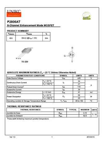
P2806AT N-Channel Enhancement Mode MOSFET PRODUCT SUMMARY V(BR)DSS RDS(ON) ID 60V 30m @VGS = 10V 34A TO-220 ABSOLUTE MAXIMUM RATINGS (TA = 25 C Unless Otherwise Noted) PARAMETERS/TEST CONDITIONS SYMBOL LIMITS UNITS VGS Gate-Source Voltage 20 V TC = 25 C 34 ID Continuous Drain Current TC = 100 C 21 A IDM 110 Pulsed Drain Current1 IAS Avalanche Current 29 EAS... See More ⇒
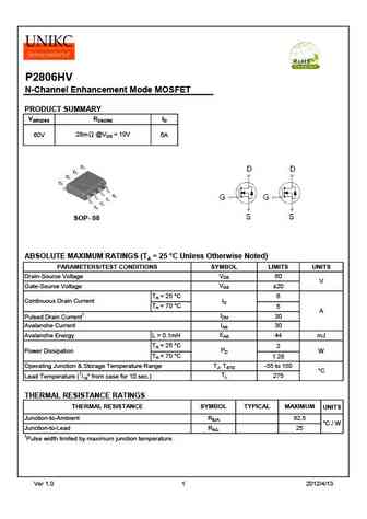
P2806HV N-Channel Enhancement Mode MOSFET PRODUCT SUMMARY V(BR)DSS RDS(ON) ID 60V 28m @VGS = 10V 6A SOP- 08 ABSOLUTE MAXIMUM RATINGS (TA = 25 C Unless Otherwise Noted) PARAMETERS/TEST CONDITIONS SYMBOL LIMITS UNITS VDS Drain-Source Voltage 60 V VGS Gate-Source Voltage 20 TA = 25 C 6 ID Continuous Drain Current TA = 70 C 5 A IDM 30 Pulsed Drain Current1 IAS... See More ⇒

P2804BDG N-Channel Enhancement Mode MOSFET PRODUCT SUMMARY V(BR)DSS RDS(ON) ID 28m @VGS = 10V 40V 25A TO-252 ABSOLUTE MAXIMUM RATINGS (TC = 25 C Unless Otherwise Noted) PARAMETERS/TEST CONDITIONS SYMBOL LIMITS UNITS VGS Gate-Source Voltage 20 V TC = 25 C 25 ID Continuous Drain Current TC = 100 C 16 A IDM 75 Pulsed Drain Current1 IAS Avalanche Current 26 EA... See More ⇒
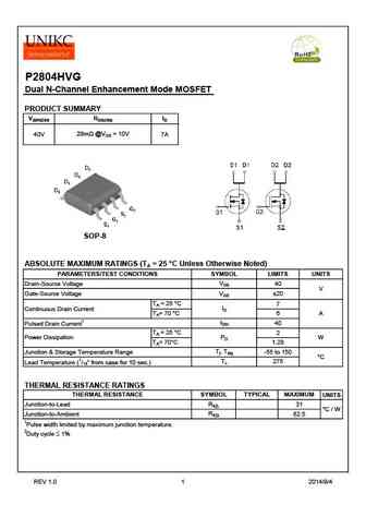
P2804HVG Dual N-Channel Enhancement Mode MOSFET PRODUCT SUMMARY V(BR)DSS RDS(ON) ID 28m @VGS = 10V 40V 7A SOP-8 ABSOLUTE MAXIMUM RATINGS (TA = 25 C Unless Otherwise Noted) PARAMETERS/TEST CONDITIONS SYMBOL LIMITS UNITS VDS Drain-Source Voltage 40 V VGS Gate-Source Voltage 20 TA = 25 C 7 ID Continuous Drain Current TA= 70 C 6 A IDM 40 Pulsed Drain Current1 ... See More ⇒
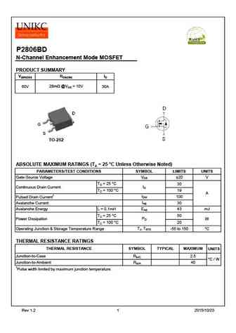
P2806BD N-Channel Enhancement Mode MOSFET PRODUCT SUMMARY V(BR)DSS RDS(ON) ID 28m @VGS = 10V 60V 30A TO-252 ABSOLUTE MAXIMUM RATINGS (TA = 25 C Unless Otherwise Noted) PARAMETERS/TEST CONDITIONS SYMBOL LIMITS UNITS VGS Gate-Source Voltage 20 V TC = 25 C 30 ID Continuous Drain Current TC = 100 C 19 A IDM 100 Pulsed Drain Current1 IAS Avalanche Current 30 EA... See More ⇒
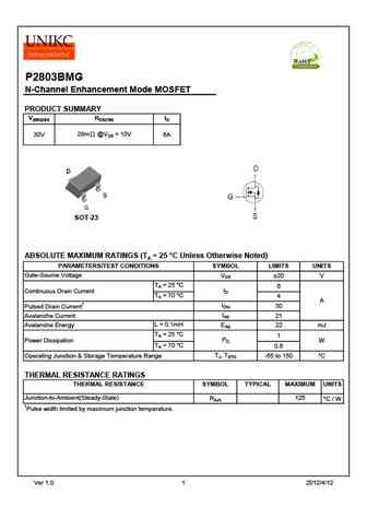
P2803BMG N-Channel Enhancement Mode MOSFET PRODUCT SUMMARY V(BR)DSS RDS(ON) ID 30V 28m @VGS = 10V 6A SOT-23 ABSOLUTE MAXIMUM RATINGS (TA = 25 C Unless Otherwise Noted) PARAMETERS/TEST CONDITIONS SYMBOL LIMITS UNITS Gate-Source Voltage VGS 20 V TA = 25 C 6 ID Continuous Drain Current TA = 70 C 4 A IDM 30 Pulsed Drain Current1 IAS Avalanche Current 21 L = 0.... See More ⇒
dh100p28 dh100p28f dh100p28i dh100p28e dh100p28b dh100p28d.pdf ![]()
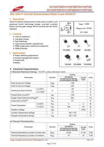
DH100P28/DH100P28F/DH100P28I DH100P28E/DH100P28B/DH100P28D 30A 100V P-channel Enhancement Mode Power MOSFET 1 Description These P-channel enhancement mode power mosfets used 2 D advanced trench technology design, provided excellent V = -100V DSS Rdson and low gate charge. Which accords with the RoHS G R = 47m DS(on) (TYP) standard. 1 3 S ID =-30A 2 Features Low on resista... See More ⇒
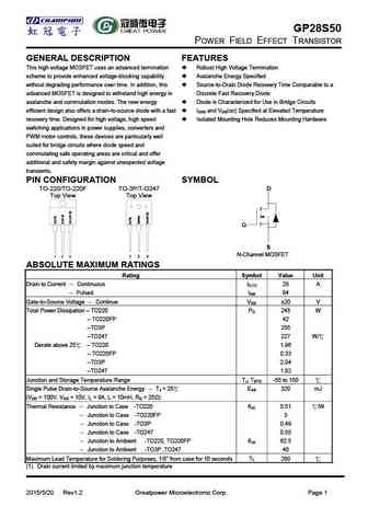
GP28S50 POWER FIELD EFFECT TRANSISTOR GENERAL DESCRIPTION FEATURES This high voltage MOSFET uses an advanced termination Robust High Voltage Termination scheme to provide enhanced voltage-blocking capability Avalanche Energy Specified without degrading performance over time. In addition, this Source-to-Drain Diode Recovery Time Comparable to a advanced MOSFET is designed to wi... See More ⇒
knp2803a knb2803a knd2803a kny2803a.pdf ![]()
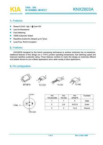
150A 30V KNX2803A N-CHANNEL MOSFET KIA KIA KIA SEMICONDUCTORS SEMICONDUCTORS SEMICONDUCTORS 1. Features R =2.2m typ. @ V =10V DS(on) GS Low On-Resistance Fast Switching 100% Avalanche Tested Repetitive Avalanche Allowed up to Tjmax Lead-Free, RoHS Compliant 2. Features KNX2803A designed by the trench processing techniques to achieve extremely l... See More ⇒
knp2804a knb2804a knd2804a.pdf ![]()
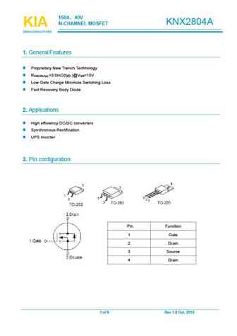
150A 40V KNX2804A N-CHANNELMOSFET KIA KIA KIA SEMICONDUCTORS SEMICONDUCTORS SEMICONDUCTORS 1.General Features Proprietary NewTrenchTechnology R =3.0m (typ.)@V =10V DS(ON),typ. GS LowGate Charge Minimize Switching Loss Fast Recovery Body Diode 2.Applications High efficiency DC/DCconverters Synchronous Rectification UPSInverter 3. Pinconfiguration Pin Function 1 Gat... See More ⇒
knp2803a knb2803a knd2803a.pdf ![]()
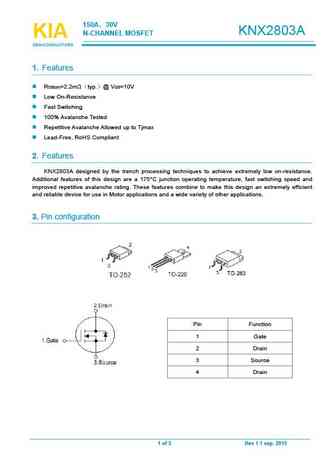
150A 30V KNX2803A N-CHANNELMOSFET KIA KIA KIA SEMICONDUCTORS SEMICONDUCTORS SEMICONDUCTORS 1. Features R =2.2m typ. @V =10V DS(on) GS LowOn-Resistance Fast Switching 100%AvalancheTested RepetitiveAvalancheAllowed up toTjmax Lead-Free, RoHSCompliant 2. Features KNX2803A designed by the trench processing techniques to achieve extremely low on-resistance. Addition... See More ⇒
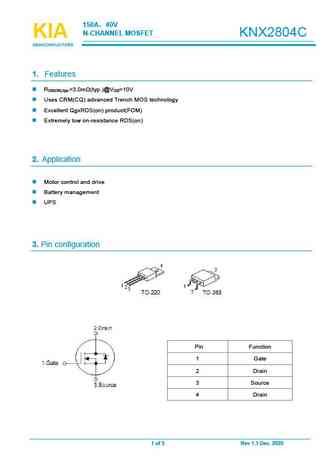
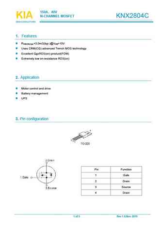
150A 40V N-CHANNEL MOSFET KNX2804C KIA KIA KIA SEMICONDUCTORS SEMICONDUCTORS SEMICONDUCTORS 1. Features R =3.0m (typ.)@V =10V DS(ON),typ. GS Uses CRM(CQ) advanced Trench MOS technology Excellent QgxRDS(on) product(FOM) Extremely low on-resistance RDS(on) 2. Application Motor control and drive Battery management UPS 3. Pin configuration Pin Func... See More ⇒
150A 40V N-CHANNELMOSFET KNX2804C KIA KIA KIA SEMICONDUCTORS SEMICONDUCTORS SEMICONDUCTORS 1. Features R =3.0m (typ.)@V =10V DS(ON),typ. GS Uses CRM(CQ) advancedTrench MOStechnology Excellent QgxRDS(on) product(FOM) Extremely lowon-resistance RDS(on) 2. Application Motor control and drive Battery management UPS 3. Pinconfiguration Pin Function 1 Gate 2 Drain 3 S... See More ⇒
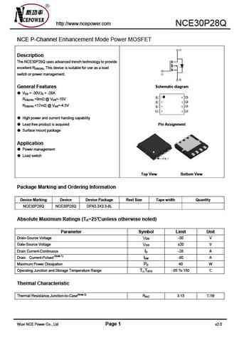
http //www.ncepower.com NCE30P28Q NCE P-Channel Enhancement Mode Power MOSFET Description The NCE30P28Q uses advanced trench technology to provide excellent RDS(ON), This device is suitable for use as a load switch or power management. Schematic diagram General Features VDS = -30V,ID = -28A RDS(ON) ... See More ⇒
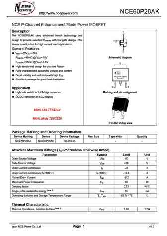
NCE60P28AK http //www.ncepower.com NCE P-Channel Enhancement Mode Power MOSFET Description The NCE60P28AK uses advanced trench technology and design to provide excellent RDS(ON) with low gate charge .This device is well suited for high current load applications. General Features VDS =-60V,ID =-28A RDS(ON) ... See More ⇒
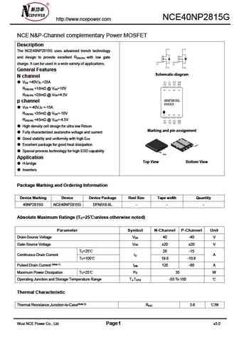
NCE40NP2815G http //www.ncepower.com NCE N&P-Channel complementary Power MOSFET Description The NCE40NP2815G uses advanced trench technology and design to provide excellent R with low gate DS(ON) charge. It can be used in a wide variety of applications. General Features Schematic diagram N channel V =40V,I =28A DS D R ... See More ⇒
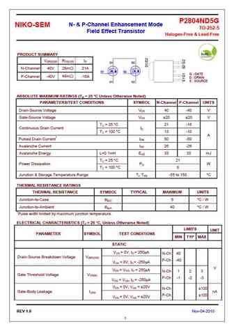
P2804ND5G N- & P-Channel Enhancement Mode NIKO-SEM TO-252-5 Field Effect Transistor Halogen-Free & Lead-Free PRODUCT SUMMARY V(BR)DSS RDS(ON) ID D1 D2 28m N-Channel 40V 21A G1 G2 G GATE 48m -16A P-Channel -40V D DRAIN S SOURCE S1 S2 ABSOLUTE MAXIMUM RATINGS (TA = 25 C Unless Otherwise Noted) PARAMETERS/TEST CONDITIONS SYMBOL N-Channel P-Channe... See More ⇒

P2804NVG N&P-Channel Enhancement Mode MOSFET PRODUCT SUMMARY V(BR)DSS RDS(ON) ID Channel 28m @VGS = 10V 40V 7A N 65m @VGS = -10V -40V -6A P SOP-8 ABSOLUTE MAXIMUM RATINGS (TA = 25 C Unless Otherwise Noted) PARAMETERS/TEST CONDITIONS SYMBOL CH. LIMITS UNITS N 40 VDS Drain-Source Voltage P -40 V N 20 VGS Gate-Source Voltage P 20 N 7 TA = 25 C P -6 ID Contin... See More ⇒
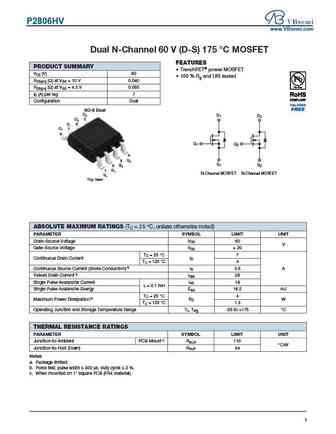
P2806HV www.VBsemi.com Dual N-Channel 60 V (D-S) 175 C MOSFET FEATURES PRODUCT SUMMARY TrenchFET power MOSFET VDS (V) 60 100 % Rg and UIS tested RDS(on) ( ) at VGS = 10 V 0.040 RDS(on) ( ) at VGS = 4.5 V 0.055 ID (A) per leg 7 Configuration Dual SO-8 Dual D2 D1 D2 D2 5 D1 6 D1 7 8 G1 G2 4 G2 3 3 S1 S2 S2 S2 2 2 G G1 1 1 N-Channel MOSFET N-Channel... See More ⇒
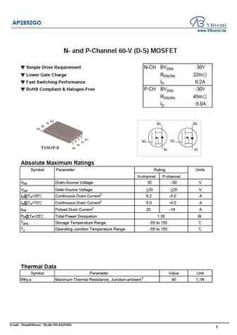
AP2852GO www.VBsemi.tw N- and P-Channel 60-V (D-S) MOSFET Simple Drive Requirement N-CH BVDSS 30V Lower Gate Charge RDS(ON) 22m Fast Switching Performance ID 6.2A RoHS Compliant & Halogen-Free P-CH BVDSS -30V RDS(ON) 45m ID -5.0A D1 D2 G2 G1 S1 S2 Absolute Maximum Ratings Symbol Parameter Rating Units N-channel P-channel VDS Drain-Source Voltage 30 -30 V VGS... See More ⇒
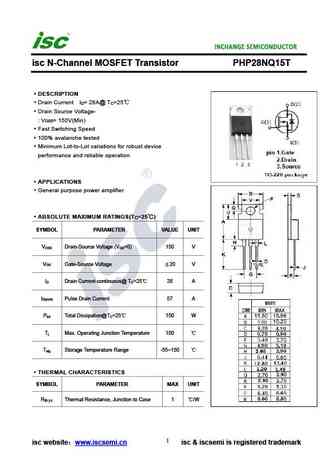
isc N-Channel MOSFET Transistor PHP28NQ15T DESCRIPTION Drain Current I = 28A@ T =25 D C Drain Source Voltage- V = 150V(Min) DSS Fast Switching Speed 100% avalanche tested Minimum Lot-to-Lot variations for robust device performance and reliable operation APPLICATIONS General purpose power amplifier ABSOLUTE MAXIMUM RATINGS(T =25 ) C SYMBOL PARAMETER VALUE ... See More ⇒
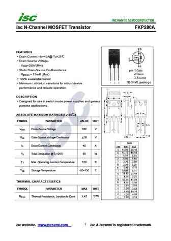
isc N-Channel MOSFET Transistor FKP280A FEATURES Drain Current I =40A@ T =25 D C Drain Source Voltage- V =280V(Min) DSS Static Drain-Source On-Resistance R = 53m (Max) DS(on) 100% avalanche tested Minimum Lot-to-Lot variations for robust device performance and reliable operation DESCRIPTION Designed for use in switch mode power supplies and general purpose ... See More ⇒
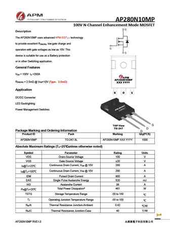
AP280N10MP 100V N-Channel Enhancement Mode MOSFET Description The AP280N10MP uses advanced APM-SGT technology to provide excellent R , low gate charge and DS(ON) operation with gate voltages as low as 10V. This device is suitable for use as a Battery protection or in other Switching application. General Features V = 100V I =280A DS D R ... See More ⇒
Detailed specifications: P216V, P217, P217A, P217B, P217G, P217V, P27, P27A, TIP142, P29, P29A, P30, P302, P303, P303A, P304, P306
Keywords - P28 pdf specs
P28 cross reference
P28 equivalent finder
P28 pdf lookup
P28 substitution
P28 replacement
