P29 Datasheet. Specs and Replacement
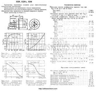
Type Designator: P29 📄📄
Material of Transistor: Ge
Polarity: PNP
Absolute Maximum Ratings
Maximum Collector Power Dissipation (Pc): 0.03 W
Maximum Collector-Base Voltage |Vcb|: 12 V
Maximum Collector Current |Ic max|: 0.1 A
Max. Operating Junction Temperature (Tj): 75 °C
Electrical Characteristics
Transition Frequency (ft): 5 MHz
Collector Capacitance (Cc): 6 pF
Forward Current Transfer Ratio (hFE), MIN: 20
Noise Figure, dB: -
P29 Substitution
- BJT ⓘ Cross-Reference Search
P29 datasheet
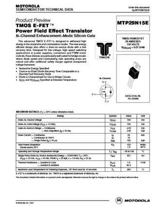
MOTOROLA Order this document SEMICONDUCTOR TECHNICAL DATA by MTP29N15E/D Product Preview MTP29N15E TMOS E-FET. Power Field Effect Transistor N Channel Enhancement Mode Silicon Gate TMOS POWER FET This advanced TMOS E FET is designed to withstand high 29 AMPERES energy in the avalanche and commutation modes. The new energy 150 VOLTS efficient design also offers a drain t... See More ⇒
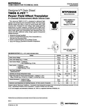
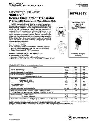
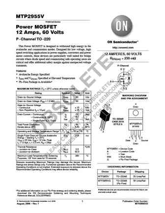
MOTOROLA Order this document SEMICONDUCTOR TECHNICAL DATA by MTP2955E/D Designer's Data Sheet MTP2955E TMOS E-FET. Motorola Preferred Device Power Field Effect Transistor P Channel Enhancement Mode Silicon Gate TMOS POWER FET This advanced TMOS E FET is designed to withstand high 12 AMPERES energy in the avalanche and commutation modes. The new energy 60 VOLTS efficie... See More ⇒
MOTOROLA Order this document SEMICONDUCTOR TECHNICAL DATA by MTP2955E/D Designer's Data Sheet MTP2955E TMOS E-FET. Motorola Preferred Device Power Field Effect Transistor P Channel Enhancement Mode Silicon Gate TMOS POWER FET This advanced TMOS E FET is designed to withstand high 12 AMPERES energy in the avalanche and commutation modes. The new energy 60 VOLTS efficie... See More ⇒
MOTOROLA Order this document SEMICONDUCTOR TECHNICAL DATA by MTP29N15E/D Product Preview MTP29N15E TMOS E-FET. Power Field Effect Transistor N Channel Enhancement Mode Silicon Gate TMOS POWER FET This advanced TMOS E FET is designed to withstand high 29 AMPERES energy in the avalanche and commutation modes. The new energy 150 VOLTS efficient design also offers a drain t... See More ⇒
... See More ⇒
MOTOROLA Order this document SEMICONDUCTOR TECHNICAL DATA by MTP2955V/D Designer's Data Sheet MTP2955V TMOS V Power Field Effect Transistor P Channel Enhancement Mode Silicon Gate TMOS POWER FET TMOS V is a new technology designed to achieve an on resis- 12 AMPERES tance area product about one half that of standard MOSFETs. This 60 VOLTS new technology more than do... See More ⇒
MOTOROLA Order this document SEMICONDUCTOR TECHNICAL DATA by MTP2955V/D Designer's Data Sheet MTP2955V TMOS V Power Field Effect Transistor P Channel Enhancement Mode Silicon Gate TMOS POWER FET TMOS V is a new technology designed to achieve an on resis- 12 AMPERES tance area product about one half that of standard MOSFETs. This 60 VOLTS new technology more than do... See More ⇒
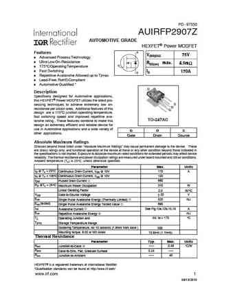
PD - 97550 AUIRFP2907Z AUTOMOTIVE GRADE HEXFET Power MOSFET D Features V(BR)DSS 75V Advanced Process Technology Ultra Low On-Resistance RDS(on) max. 4.5m G 175 C Operating Temperature Fast Switching ID 170A S Repetitive Avalanche Allowed up to Tjmax Lead-Free, RoHS Compliant Automotive Qualified * D Description Specifically designed for... See More ⇒
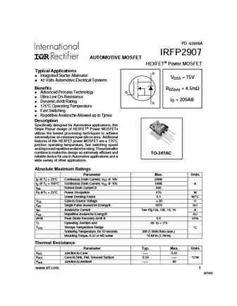
PD -93906A IRFP2907 AUTOMOTIVE MOSFET HEXFET Power MOSFET Typical Applications D Integrated Starter Alternator VDSS = 75V 42 Volts Automotive Electrical Systems Benefits RDS(on) = 4.5m Advanced Process Technology G Ultra Low On-Resistance ID = 209AV Dynamic dv/dt Rating S 175 C Operating Temperature Fast Switching Repetitive Avalanche Allowed up to Tjmax Descript... See More ⇒
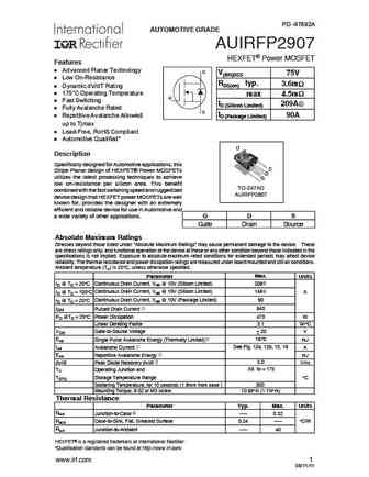
PD -97692A AUTOMOTIVE GRADE AUIRFP2907 HEXFET Power MOSFET Features l Advanced Planar Technology D V(BR)DSS 75V l Low On-Resistance RDS(on) typ. 3.6m l Dynamic dV/dT Rating l 175 C Operating Temperature max 4.5m G l Fast Switching ID (Silicon Limited) 209A l Fully Avalanche Rated S ID (Package Limited) 90A l Repetitive Avalanche Allowed up to Tjmax l Lead-Free, R... See More ⇒
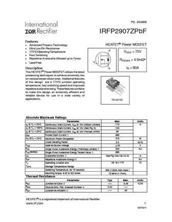
PD - 95480B IRFP2907ZPbF Features HEXFET Power MOSFET l Advanced Process Technology l Ultra Low On-Resistance D l 175 C Operating Temperature VDSS = 75V l Fast Switching l Repetitive Avalanche Allowed up to Tjmax RDS(on) = 4.5m G l Lead-Free ID = 90A S Description This HEXFET Power MOSFET utilizes the latest processing techniques to achieve extremely low on-resistan... See More ⇒
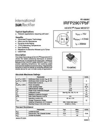
PD -95050C IRFP2907PbF HEXFET Power MOSFET Typical Applications D Telecom applications requiring soft start VDSS = 75V Benefits RDS(on) = 4.5m Advanced Process Technology G Ultra Low On-Resistance Dynamic dv/dt Rating ID = 209A S 175 C Operating Temperature Fast Switching Repetitive Avalanche Allowed up to Tjmax Lead-Free Description This Stripe Planar design... See More ⇒
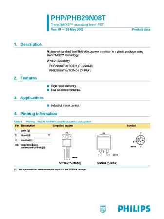
PHP/PHB29N08T TrenchMOS standard level FET Rev. 01 29 May 2002 Product data 1. Description N-channel standard level field-effect power transistor in a plastic package using TrenchMOS technology. Product availability PHP29N08T in SOT78 (TO-220AB) PHB29N08T in SOT404 (D2-PAK). 2. Features High noise immunity Low on-state resistance. 3. Applications Industrial motor cont... See More ⇒
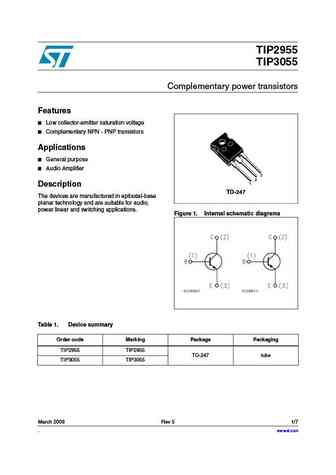
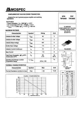
TIP2955 TIP3055 Complementary power transistors Features Low collector-emitter saturation voltage Complementary NPN - PNP transistors Applications General purpose Audio Amplifier 3 2 1 Description TO-247 The devices are manufactured in epitaxial-base planar technology and are suitable for audio, power linear and switching applications. Figure 1. Internal sche... See More ⇒
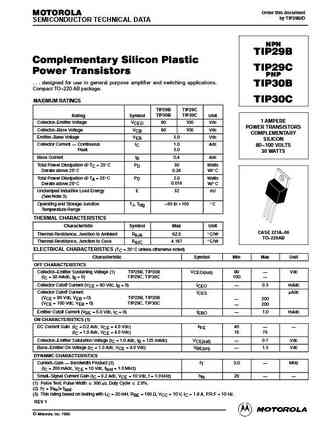
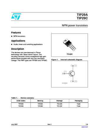
TIP29A TIP29C NPN power transistors . Features NPN transistors Applications Audio, linear and switching applications 3 Description 2 1 The devices are manufactured in Planar TO-220 technology with Base Island layout. The resulting transistor shows exceptional high gain performance coupled with very low saturation Figure 1. Internal schematic diagram voltage. ... See More ⇒
tip29a-tip29c tip30a-tip30c.pdf ![]()
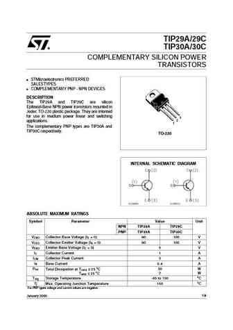
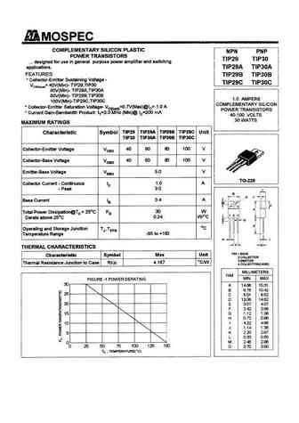
TIP29A/29C TIP30A/30C COMPLEMENTARY SILICON POWER TRANSISTORS STMicroelectronics PREFERRED SALESTYPES COMPLEMENTARY PNP - NPN DEVICES DESCRIPTION The TIP29A and TIP29C are silicon Epitaxial-Base NPN power transistors mounted in Jedec TO-220 plastic package. They are intented for use in medium power linear and switching 3 2 applications. 1 The complementary PNP types ar... See More ⇒
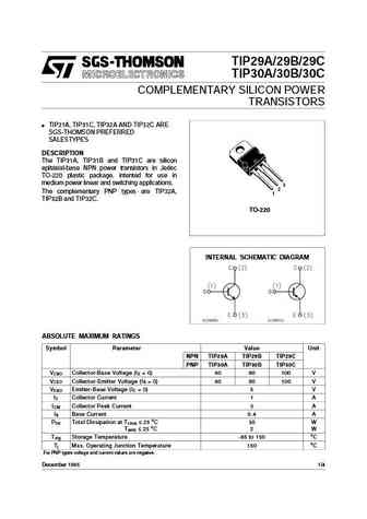
TIP29A/29B/29C TIP30A/30B/30C COMPLEMENTARY SILICON POWER TRANSISTORS TIP31A, TIP31C, TIP32A AND TIP32C ARE SGS-THOMSON PREFERRED SALESTYPES DESCRIPTION The TIP31A, TIP31B and TIP31C are silicon epitaxial-base NPN power transistors in Jedec TO-220 plastic package, intented for use in medium power linear and switching applications. 3 2 The complementary PNP types are TIP32A, 1... See More ⇒
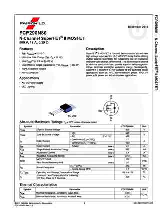
December 2015 FCP290N80 N-Channel SuperFET II MOSFET 800 V, 17 A, 0.29 Features Description Typ. RDS(on) = 0.245 SuperFET II MOSFET is Fairchild Semiconductor s brand-new high voltage super-junction (SJ) MOSFET family that is utilizing Ultra Low Gate Charge (Typ. Qg = 58 nC) charge balance technology for outstanding low on-resistance Low Eoss (Typ. 5.6 uJ ... See More ⇒
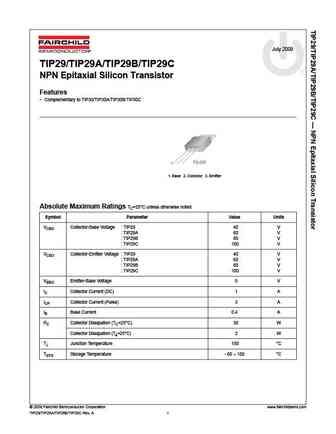
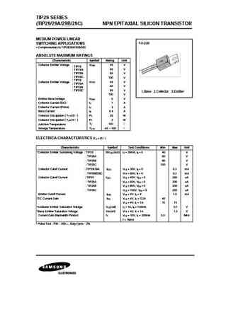
July 2008 TIP29/TIP29A/TIP29B/TIP29C NPN Epitaxial Silicon Transistor Features Complementary to TIP30/TIP30A/TIP30B/TIP30C 1. Base 2. Collector 3. Emitter Absolute Maximum Ratings TC=25 C unless otherwise noted Symbol Parameter Value Units VCBO Collector-Base Voltage TIP29 40 V TIP29A 60 V TIP29B 80 V TIP29C 100 V VCEO Collector-Emitter Voltage TIP29 40 V TIP... See More ⇒
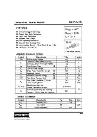
SFP2955 Advanced Power MOSFET FEATURES BVDSS = -60 V Avalanche Rugged Technology RDS(on) = 0.3 Rugged Gate Oxide Technology Lower Input Capacitance ID = -9.4 A Improved Gate Charge 175oC Opereting Temperature TO-220 Extended Safe Operating Area Lower Leakage Current -10 A (Max.) @ VDS = -60V Low RDS(ON) 0.22 (Typ.) 1 2 3 1.Gate 2. Drain 3. Source Absolu... See More ⇒
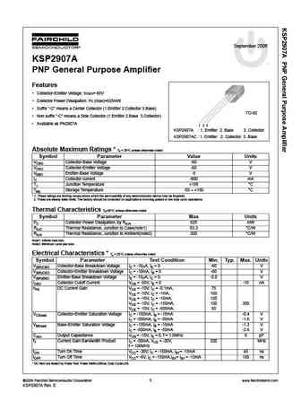
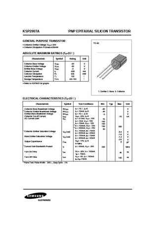
September 2006 KSP2907A tm PNP General Purpose Amplifier Features Collector-Emitter Voltage VCEO= 60V Collector Power Dissipation PC (max)=625mW Suffix -C means a Center Collector (1.Emitter 2.Collector 3.Base) TO-92 Non suffix -C means a Side Collector (1.Emitter 2.Base 3.Collector) Available as PN2907A 1 2 3 KSP2907A 1. Emitter 2. Base 3. Coll... See More ⇒
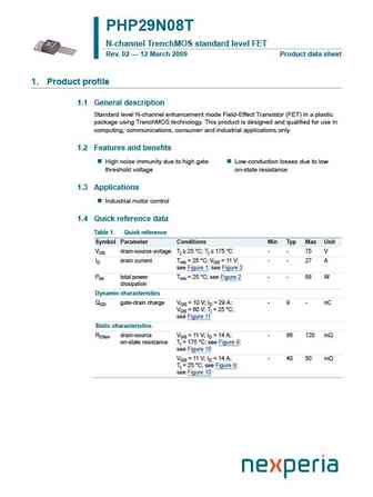
PHP29N08T N-channel TrenchMOS standard level FET Rev. 02 12 March 2009 Product data sheet 1. Product profile 1.1 General description Standard level N-channel enhancement mode Field-Effect Transistor (FET) in a plastic package using TrenchMOS technology. This product is designed and qualified for use in computing, communications, consumer and industrial applications only. 1.2 Featu... See More ⇒
KSP2907A PNP EPITAXIAL SILICON TRANSISTOR GENERAL PURPOSE TRANSISTOR TO-92 Collector-Emitter Voltage VCEO= 60V Collector Dissipation PC(max)=625mW ABSOLUTE MAXIMUM RATINGS (T =25 ) A Characteristic Symbol Rating Unit Collector-Base Voltage VCBO -60 V Collector-Emitter Voltage VCEO -60 V Emitter-Base Voltage VEBO -5 V Collector Current IC -600 mA Collector Dissipation PC 6... See More ⇒
TIP29 SERIES (TIP29/29A/29B/29C) NPN EPITAXIAL SILICON TRANSISTOR MEDIUM POWER LINEAR TO-220 SWITCHING APPLICATIONS Complementary to TIP30/30A/30B/30C ABSOLUTE MAXIMUM RATINGS Characteristic Symbol Rating Unit Collector Emitter Voltage VCBO 40 V TIP29 60 V TIP29A TIP29B 80 V TIP29C 100 V TIP29 Collector Emitter Voltage VCEO 40 V TIP29A 60 V TIP29B TI... See More ⇒
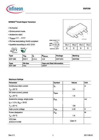
BSP 299 SIPMOS Small-Signal Transistor N channel Enhancement mode Avalanche rated VGS(th)= 2.1 ... 4.0 V Pin 1 Pin 2 Pin 3 Pin 4 G D S D Type VDS ID RDS(on) Package Marking BSP 299 500 V 0.4 A 4 SOT-223 BSP 299 Type Ordering Code Tape and Reel Information BSP 299 Q67000-S225 E6327 Maximum Ratings Parameter Symbol Values Unit Continuous drain current ID A TA... See More ⇒
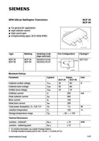
NPN Silicon Darlington Transistors BCP 29 BCP 49 For general AF applications High collector current High current gain Complementary types BCP 28/48 (PNP) Type Marking Ordering Code Pin Configuration Package1) (tape and reel) BCP 29 BCP 29 Q62702-C2136 SOT-223 BCP 49 BCP 49 Q62702-C2137 Maximum Ratings Parameter Symbol Values Unit BCP 29 BCP 49 Collector-emitter voltage VCE0 3... See More ⇒
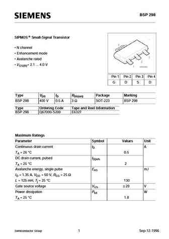
BSP 298 SIPMOS Small-Signal Transistor N channel Enhancement mode Avalanche rated VGS(th)= 2.1 ... 4.0 V Pin 1 Pin 2 Pin 3 Pin 4 G D S D Type VDS ID RDS(on) Package Marking BSP 298 400 V 0.5 A 3 SOT-223 BSP 298 Type Ordering Code Tape and Reel Information BSP 298 Q67000-S200 E6327 Maximum Ratings Parameter Symbol Values Unit Continuous drain current ID A TA... See More ⇒
BSP299 SIPMOS Small-Signal Transistor N channel Enhancement mode Avalanche rated VGS(th)= 2.1 ... 4.0 V Pb-free lead plating; RoHS compliant Qualified according to AEC Q101 Pin 1 Pin 2 Pin 3 Pin 4 G D S D Type VDS ID RDS(on) Package Marking BSP 299 500 V 0.4 A 4 SOT-223 BSP299 Type Pb-free Tape and Reel Information BSP 299 Yes L6327 Maximum Ratings ... See More ⇒
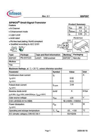
Rev. 2.1 BSP297 SIPMOS Small-Signal-Transistor Product Summary Feature VDS 200 V N-Channel RDS(on) 1.8 Enhancement mode ID 0.66 A Logic Level PG-SOT223 dv/dt rated Pb-free lead plating; RoHS compliant 4 Qualified according to AEC Q101 3 2 1 VPS05163 Packaging Type Package Tape and Reel Information Marking PG-SOT223 BSP297 L6327 1000 pcs/reel... See More ⇒
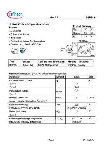
Rev 2.2 BSP295 SIPMOS Small-Signal-Transistor Product Summary Feature VDS 60 V N-Channel RDS(on) 0.3 Enhancement mode ID 1.8 A dv/dt rated PG-SOT223 Pb-free lead plating; RoHS compliant Qualified according to AEC Q101 4 3 2 1 VPS05163 Marking Type Package Tape and Reel Information Marking Packaging PG-SOT223 BSP295 L6327 1000 pcs/reel BSP295 Non dry Maximum... See More ⇒
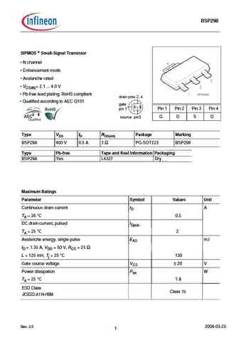
BSP298 SIPMOS Small-Signal Transistor N channel Enhancement mode Avalanche rated VGS(th)= 2.1 ... 4.0 V Pb-free lead plating; RoHS compliant Qualified according to AEC Q101 Pin 1 Pin 2 Pin 3 Pin 4 G D S D Type VDS ID RDS(on) Package Marking BSP298 400 V 0.5 A 3 PG-SOT223 BSP298 Type Pb-free Tape and Reel Information Packaging BSP298 Yes L6327 Dry Max... See More ⇒
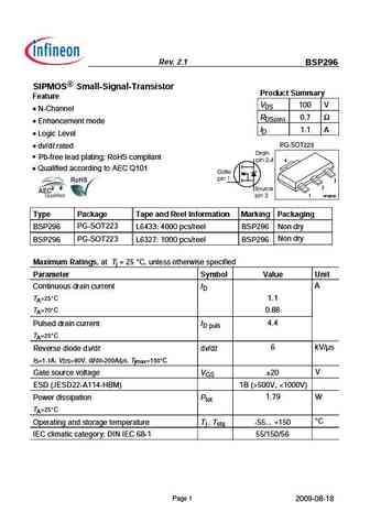
Rev. 2.1 BSP296 SIPMOS Small-Signal-Transistor Product Summary Feature VDS 100 V N-Channel RDS(on) 0.7 Enhancement mode ID 1.1 A Logic Level PG-SOT223 dv/dt rated Pb-free lead plating; RoHS compliant 4 Qualified according to AEC Q101 3 2 1 VPS05163 Type Package Tape and Reel Information Marking Packaging PG-SOT223 BSP296 L6433 4000 pcs/reel ... See More ⇒
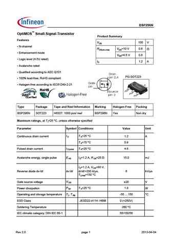
BSP296N OptiMOS Small-Signal-Transistor Product Summary Features VDS 100 V N-channel RDS(on),max VGS=10 V 0.6 W Enhancement mode VGS=4.5 V 0.8 Logic level (4.5V rated) ID 1.2 A Avalanche rated Qualified according to AEC Q101 PG-SOT223 100% lead-free; RoHS compliant Halogen-free according to IEC61249-2-21 Type Package Tape and Reel Informati... See More ⇒
tip29-a-b-c tip30-a-b-c to-220.pdf ![]()
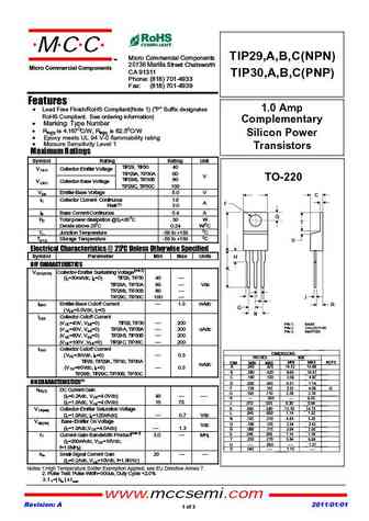
MCC Micro Commercial Components TM TIP29,A,B,C(NPN) 20736 Marilla Street Chatsworth Micro Commercial Components CA 91311 TIP30,A,B,C(PNP) Phone (818) 701-4933 Fax (818) 701-4939 Features Lead Free Finish/RoHS Compliant(Note 1) ("P" Suffix designates 1.0 Amp RoHS Compliant. See ordering information) Complementary Marking Type Number Rth(jc) is 4.167OC/W, Rth(ja) i... See More ⇒
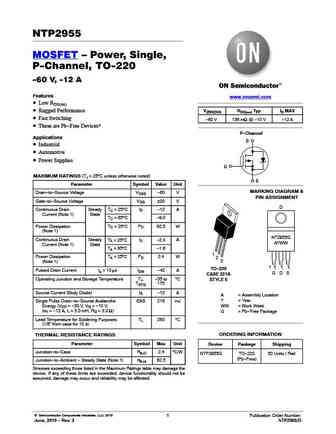
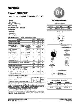
NTP2955 MOSFET Power, Single, P-Channel, TO-220 -60 V, -12 A Features www.onsemi.com Low RDS(on) Rugged Performance V(BR)DSS RDS(on) Typ ID MAX Fast Switching -60 V 156 mW @ -10 V -12 A These are Pb-Free Devices* P-Channel Applications D Industrial Automotive Power Supplies G MAXIMUM RATINGS (TJ = 25 C unless otherwise noted) S Parameter Symb... See More ⇒
NTP2955 Power MOSFET -60 V, -12 A, Single P-Channel, TO-220 Features Low RDS(on) http //onsemi.com Rugged Performance Fast Switching V(BR)DSS RDS(on) Typ ID MAX Pb-Free Package is Available* -60 V 156 mW @ -10 V -12 A Applications Industrial P-Channel Automotive D Power Supplies MAXIMUM RATINGS (TJ = 25 C unless otherwise noted) Parameter Symbol Va... See More ⇒
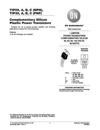
TIP29, A, B, C (NPN), TIP30, A, B, C (PNP) Complementary Silicon Plastic Power Transistors Designed for use in general purpose amplifier and switching applications. Compact TO-220 AB package. http //onsemi.com Features 1 AMPERE Pb-Free Packages are Available* POWER TRANSISTORS COMPLEMENTARY SILICON 40, 60, 80, 100 VOLTS, 80 WATTS MARKING DIAGRAM 4 TO-220AB TIPxxxG CASE 2... See More ⇒
Is Now Part of To learn more about ON Semiconductor, please visit our website at www.onsemi.com Please note As part of the Fairchild Semiconductor integration, some of the Fairchild orderable part numbers will need to change in order to meet ON Semiconductor s system requirements. Since the ON Semiconductor product management systems do not have the ability to manage part nomenclatur... See More ⇒
ksp2907abu ksp2907ata ksp2907atf ksp2907acta.pdf ![]()
Is Now Part of To learn more about ON Semiconductor, please visit our website at www.onsemi.com Please note As part of the Fairchild Semiconductor integration, some of the Fairchild orderable part numbers will need to change in order to meet ON Semiconductor s system requirements. Since the ON Semiconductor product management systems do not have the ability to manage part nomenclatur... See More ⇒
tip29g tip29ag tip29bg tip29cg tip30g tip30ag tip30bg tip30cg.pdf ![]()
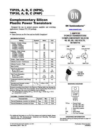
TIP29, A, B, C (NPN), TIP30, A, B, C (PNP) Complementary Silicon Plastic Power Transistors Designed for use in general purpose amplifier and switching applications. Compact TO-220 package. www.onsemi.com Features 1 AMPERE These Devices are Pb-Free and are RoHS Compliant* POWER TRANSISTORS MAXIMUM RATINGS COMPLEMENTARY SILICON Rating Symbol Value Unit 40, 60, 80, 100 VOLTS, Col... See More ⇒
tip29 tip29a tip29b tip29c tip30 tip30a tip30b tip30c.pdf ![]()
TIP29, A, B, C (NPN), TIP30, A, B, C (PNP) Complementary Silicon Plastic Power Transistors Designed for use in general purpose amplifier and switching applications. Compact TO-220 package. www.onsemi.com Features 1 AMPERE These Devices are Pb-Free and are RoHS Compliant* POWER TRANSISTORS MAXIMUM RATINGS COMPLEMENTARY SILICON Rating Symbol Value Unit 40, 60, 80, 100 VOLTS, Col... See More ⇒
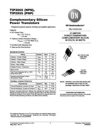
TIP3055 (NPN), TIP2955 (PNP) Complementary Silicon Power Transistors Designed for general-purpose switching and amplifier applications. http //onsemi.com Features DC Current Gain - 15 AMPERE hFE = 20 - 70 @ IC POWER TRANSISTORS = 4.0 Adc COMPLEMENTARY SILICON Collector-Emitter Saturation Voltage - 60 VOLTS, 90 WATTS VCE(sat) = 1.1 Vdc (Max) @ IC = 4.0 Adc Excell... See More ⇒
Is Now Part of To learn more about ON Semiconductor, please visit our website at www.onsemi.com Please note As part of the Fairchild Semiconductor integration, some of the Fairchild orderable part numbers will need to change in order to meet ON Semiconductor s system requirements. Since the ON Semiconductor product management systems do not have the ability to manage part nomenclatur... See More ⇒
MTP2955V Preferred Device Power MOSFET 12 Amps, 60 Volts P-Channel TO-220 This Power MOSFET is designed to withstand high energy in the http //onsemi.com avalanche and commutation modes. Designed for low voltage, high speed switching applications in power supplies, converters and power 12 AMPERES, 60 VOLTS motor controls, these devices are particularly well suited for bridge RDS(on) ... See More ⇒
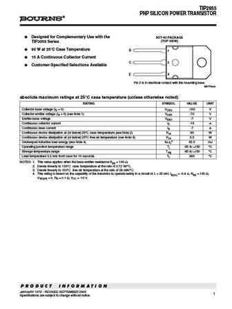
TIP2955 PNP SILICON POWER TRANSISTOR Designed for Complementary Use with the SOT-93 PACKAGE (TOP VIEW) TIP3055 Series 90 W at 25 C Case Temperature B 1 15 A Continuous Collector Current C 2 Customer-Specified Selections Available 3 E Pin 2 is in electrical contact with the mounting base. MDTRAAA absolute maximum ratings at 25 C case temperature (unless otherwi... See More ⇒
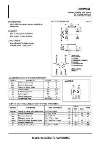
RT2P29M Composite Transistor With Resistor For Switching Application Silicon PNP Epitaxial Type OUTLINE DRAWING Unit mm DESCRIPTION 2.1 RT2P29M is composite transistor with built-in 1.25 bias resistor. FEATURE Built-in bias resistor (R2=100k ) Mini package for easy mounting APPLICATION Inverted circuit, Switching circuit, Interface circu... See More ⇒
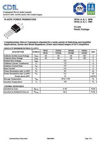
Continental Device India Limited An ISO/TS 16949, ISO 9001 and ISO 14001 Certified Company PLASTIC POWER TRANSISTORS TIP29, A, B, C NPN TIP30, A, B, C PNP TO-220 Plastic Package Complementary Silicon Transistors intended for a wide variety of Switching and Amplifier Applications, Series and Shunt Regulators, Driver and Output stages of Hi-Fi Amplifiers ABSOLUTE MAXIMUM RATINGS (Ta=25 ... See More ⇒
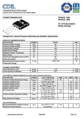
Continental Device India Limited An ISO/TS 16949, ISO 9001 and ISO 14001 Certified Company POWER TRANSISTORS TIP2955F PNP TIP3055F NPN TO- 3P Fully Isolated Plastic Package B C E Designed for General Purpose Switching and Amplifier Applications ABSOLUTE MAXIMUM RATINGS DESCRIPTION SYMBOL VALUE UNIT Collector-Emitter Voltage VCEO 60 V Collector-Emitter Voltage VCER 70 V Collector-... See More ⇒
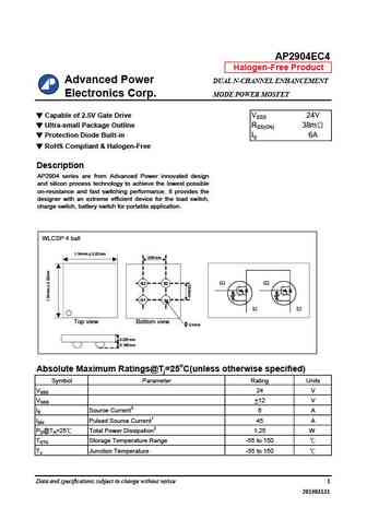
AP2904EC4 Halogen-Free Product Advanced Power DUAL N-CHANNEL ENHANCEMENT Electronics Corp. MODE POWER MOSFET Capable of 2.5V Gate Drive VSSS 24V Ultra-small Package Outline RSS(ON) 38m Protection Diode Built-in IS 6A RoHS Compliant & Halogen-Free Description AP2904 series are from Advanced Power innovated design and silicon process technology to achieve the lowest po... See More ⇒
AP2910EC4 Halogen-Free Product Advanced Power DUAL N-CHANNEL ENHANCEMENT Electronics Corp. MODE POWER MOSFET Capable of 2.5V Gate Drive VSSS 24V Ultra-small Package Outline RSS(ON) 22.5m Protection Diode Built-in IS 9A RoHS Compliant & Halogen-Free Description AP2910 series are from Advanced Power innovated design and silicon process technology to achieve the lowest ... See More ⇒
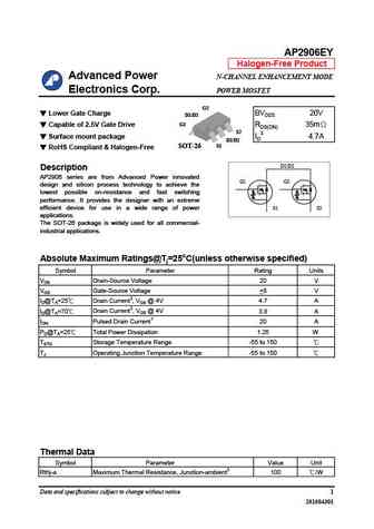
AP2906EY Halogen-Free Product Advanced Power N-CHANNEL ENHANCEMENT MODE Electronics Corp. POWER MOSFET G2 Lower Gate Charge BVDSS 20V D1/D2 G1 Capable of 2.5V Gate Drive RDS(ON) 35m S2 Surface mount package ID3 4.7A D1/D2 S1 SOT-26 RoHS Compliant & Halogen-Free D1/D2 Description AP2906 series are from Advanced Power innovated G1 G2 design and silicon process... See More ⇒
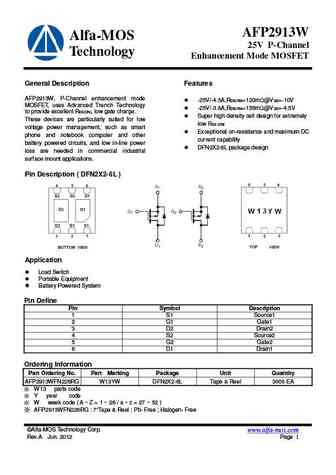
AFP2913W Alfa-MOS 25V P-Channel Technology Enhancement Mode MOSFET General Description Features AFP2913W, P-Channel enhancement mode -25V/-4.5A,RDS(ON)=120m @VGS=-10V MOSFET, uses Advanced Trench Technology -25V/-3.8A,RDS(ON)=155m @VGS=-4.5V to provide excellent RDS(ON), low gate charge. Super high density cell design for extremely These devices are particularly s... See More ⇒
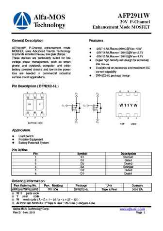
AFP2911W Alfa-MOS 20V P-Channel Technology Enhancement Mode MOSFET General Description Features AFP2911W, P-Channel enhancement mode -20V/-4.5A,RDS(ON)=96m @VGS=-4.5V MOSFET, uses Advanced Trench Technology -20V/-3.8A,RDS(ON)=128m @VGS=-2.5V to provide excellent RDS(ON), low gate charge. -20V/-2.5A,RDS(ON)=180m @VGS=-1.8V These devices are particularly suited fo... See More ⇒
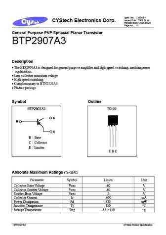
Spec. No. C317A3-H Issued Date 2002.06.11 CYStech Electronics Corp. Revised Date 2005.06.29 Page No. 1/5 General Purpose PNP Epitaxial Planar Transistor BTP2907A3 Description The BTP2907A3 is designed for general purpose amplifier and high-speed switching, medium power applications. Low collector saturation voltage High speed switching. Complementa... See More ⇒
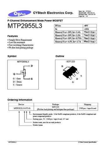
Spec. No. C733L3 Issued Date 2012.02.14 CYStech Electronics Corp. Revised Date 2014.07.25 Page No. 1/8 P-Channel Enhancement Mode Power MOSFET BVDSS -60V MTP2955L3 ID -4.8A 75m (typ.) RDSON@VGS=-10V, ID=-2.4A RDSON@VGS=-10V, ID=-1.5A 74m (typ.) Features 70m (typ.) RDSON@VGS=-10V, ID=-0.75A Simple Drive Requirement RDSON@VGS=-4.5V, ID=-1.7A 99m... See More ⇒
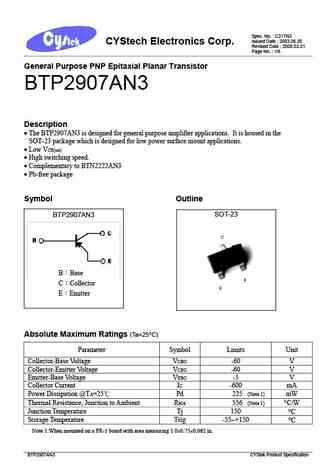
Spec. No. C317N3 Issued Date 2003.06.30 CYStech Electronics Corp. Revised Date 2008.03.21 Page No. 1/6 General Purpose PNP Epitaxial Planar Transistor BTP2907AN3 Description The BTP2907AN3 is designed for general purpose amplifier applications. It is housed in the SOT-23 package which is designed for low power surface mount applications. Low V CE(sat) ... See More ⇒
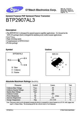
Spec. No. C317L3-H Issued Date 2003.04.15 CYStech Electronics Corp. Revised Date 2006.07.04 Page No. 1/5 General Purpose PNP Epitaxial Planar Transistor BTP2907AL3 Description The BTP2907AL3 is designed for general purpose amplifier applications. It is housed in the SOT-223 package which is designed for medium power surface mount applications. Low V CE(sat)... See More ⇒
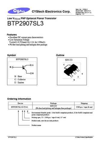
Spec. No. C824L3 Issued Date 2003.07.31 CYStech Electronics Corp. Revised Date 2013.11.12 Page No. 1/7 Low V PNP Epitaxial Planar Transistor CE(sat) BTP2907SL3 Features Excellent DC current gain characteristics Low Saturation Voltage V (sat)=-0.5V(max) (I =-1A, I =-100mA). CE C B Pb-free lead plating and halogen-free package Symbol Outline BTP2907SL3... See More ⇒
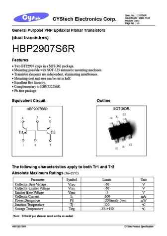
Spec. No. C317S6R Issued Date 2006.11.08 CYStech Electronics Corp. Revised Date Page No. 1/5 General Purpose PNP Epitaxial Planar Transistors (dual transistors) HBP2907S6R Features Two BTP2907 chips in a SOT-363 package. Mounting possible with SOT-323 automatic mounting machines. Transistor elements are independent, eliminating interference. Mount... See More ⇒
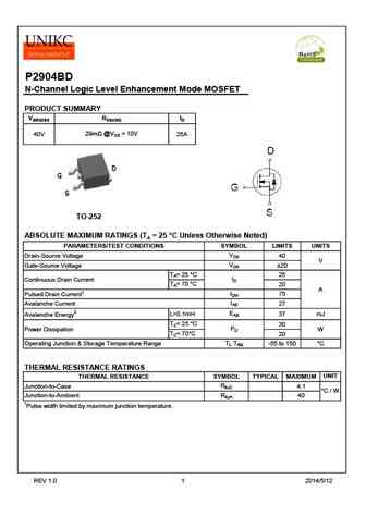
P2904BD N-Channel Logic Level Enhancement Mode MOSFET PRODUCT SUMMARY V(BR)DSS RDS(ON) ID 29m @VGS = 10V 40V 25A TO-252 ABSOLUTE MAXIMUM RATINGS (TA = 25 C Unless Otherwise Noted) PARAMETERS/TEST CONDITIONS SYMBOL LIMITS UNITS VDS Drain-Source Voltage 40 V VGS Gate-Source Voltage 20 TA= 25 C 25 ID Continuous Drain Current TA= 70 C 20 A IDM 75 Pulsed Drain ... See More ⇒
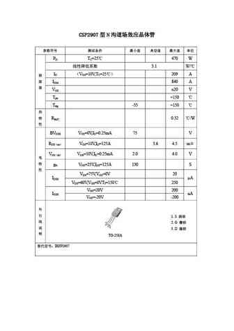
CSP2907 N PD TC=25 470 W 3.1 W/ ID VGS=10V,TC=25 209 A IDM 840 A VGS 20 V Tjm +150 Tstg -55 +150 RthJC 0.32 /W BVDSS VGS=0V,ID=0.25mA 75 V RDS on VGS=10V,ID=125A 3.6 4.5 m VGS th VDS=10V,ID=0.25mA 2.0 4... See More ⇒
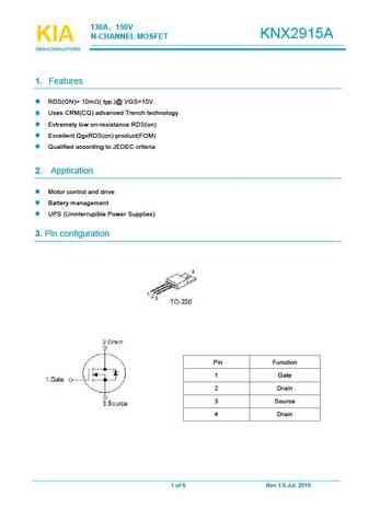
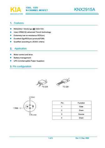
130A 150V N-CHANNELMOSFET KNX2915A KIA KIA KIA SEMICONDUCTORS SEMICONDUCTORS SEMICONDUCTORS 1. Features RDS(ON)=10m ( typ.)@VGS=10V Uses CRM(CQ) advancedTrench technology Extremely lowon-resistance RDS(on) Excellent QgxRDS(on) product(FOM) Qualified according to JEDECcriteria 2. Application Motor control and drive Battery management UPS(UninterrupiblePower Supplies)... See More ⇒
knb2910a knp2910a knh2910a.pdf ![]()
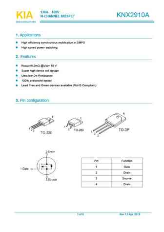
130A 100V KNX2910A N-CHANNELMOSFET KIA KIA KIA SEMICONDUCTORS SEMICONDUCTORS SEMICONDUCTORS 1.Applications High efficiency synchronous rectification in SMPS High speed power switching 2. Features R =5.0m @V =10 V DS(on) GS Super high dense cell design Ultra lowOn-Resistance 100%avalanchetested Lead Free and Green devices available (RoHSCompliant) 3. Pinconfiguratio... See More ⇒
130A 150V N-CHANNEL MOSFET KNX2915A KIA KIA KIA SEMICONDUCTORS SEMICONDUCTORS SEMICONDUCTORS 1. Features RDS(ON)= 10m ( typ.)@ VGS=10V Uses CRM(CQ) advanced Trench technology Extremely low on-resistance RDS(on) Excellent QgxRDS(on) product(FOM) Qualified according to JEDEC criteria 2. Application Motor control and drive Battery management UPS... See More ⇒
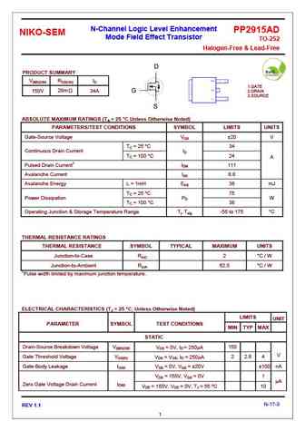
N-Channel Logic Level Enhancement PP2915AD NIKO-SEM Mode Field Effect Transistor TO-252 Halogen-Free & Lead-Free D PRODUCT SUMMARY V(BR)DSS RDS(ON) ID 1.GATE 29m 150V 34A G 2.DRAIN 3.SOURCE S ABSOLUTE MAXIMUM RATINGS (TA = 25 C Unless Otherwise Noted) PARAMETERS/TEST CONDITIONS SYMBOL LIMITS UNITS Gate-Source Voltage VGS 20 V TC = 25 C 34 Continuous Dra... See More ⇒
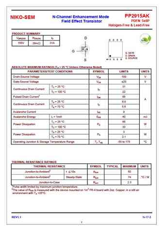
PP2915AK N-Channel Enhancement Mode NIKO-SEM PDFN 5x6P Field Effect Transistor Halogen-Free & Lead-Free PRODUCT SUMMARY V(BR)DSS RDS(ON) ID D D D D D 150V 29m 31A G G. GATE D. DRAIN S. SOURCE #1 S S S G S ABSOLUTE MAXIMUM RATINGS (TA = 25 C Unless Otherwise Noted) PARAMETERS/TEST CONDITIONS SYMBOL LIMITS UNITS Drain-Source Voltage VDS 150 V Gate-Source Vo... See More ⇒
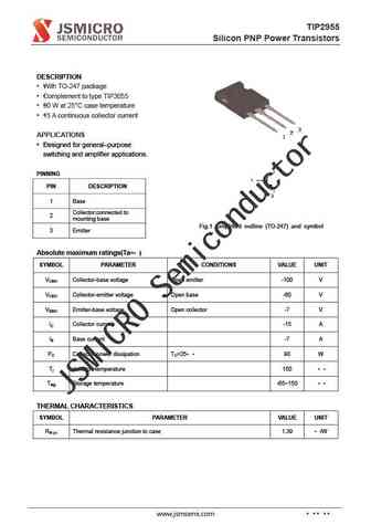
TIP2955 Silicon PNP Power Transistors DESCRIPTION With TO-247 package Complement to type TIP3055 90 W at 25 C case temperature 15 A continuous collector current APPLICATIONS Designed for general purpose switching and amplifier applications. PINNING PIN DESCRIPTION 1 Base Collector;connected to 2 mounting base Fig.1 simplified outline (TO-247) and symbol... See More ⇒
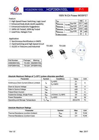
HGB290N10SL , HGP290N10SL P-1 100V N-Ch Power MOSFET Feature 100 V VDS High Speed Power Switching, Logic Level 22.7 RDS(on),typ TO-263 VGS=10V m Enhanced Body diode dv/dt capability VGS=4.5V 27.7 RDS(on),typ m Enhanced Avalanche Ruggedness 23.0 RDS(on),typ TO-220 VGS=10V m 100% UIS Tested, 100% Rg Tested VGS=4.5V 28 RDS(on),typ m Lead Free, Hal... See More ⇒
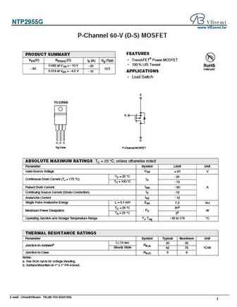
NTP2955G www.VBsemi.tw P-Channel 60-V (D-S) MOSFET FEATURES PRODUCT SUMMARY VDS (V) RDS(on) ( ) TrenchFET Power MOSFET ID (A) Qg (Typ) 100 % UIS Tested 0.062 at VGS = - 10 V - 20 - 60 12.5 0.074 at VGS = - 4.5 V - 15 APPLICATIONS Load Switch S TO-220AB G D G D S Top View P-Channel MOSFET ABSOLUTE MAXIMUM RATINGS TC = 25 C, unless otherwise noted Parameter S... See More ⇒
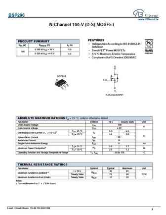
BSP296 www.VBsemi.tw N-Channel 100-V (D-S) MOSFET FEATURES PRODUCT SUMMARY Halogen-free According to IEC 61249-2-21 VDS (V) RDS(on) ( )ID (A) Definition 0.100 at VGS = 10 V 5.0 TrenchFET Power MOSFETs 100 0.120 at VGS = 4.5 V 4.5 175 C Maximum Junction Temperature Compliant to RoHS Directive 2002/95/EC D SOT-223 D G S D G S N-Channel MOSFET A... See More ⇒
INCHANGE Semiconductor isc N-Channel MOSFET Transistor FCP290N80 FEATURES With TO-220 packaging Low switching loss Ultra low gate charge Easy to use 100% avalanche tested Minimum Lot-to-Lot variations for robust device performance and reliable operationz APPLICATIONS Switching applications AC-DC converters LED lighting Uninterruptible power supply ABSOLU... See More ⇒
isc Silicon NPN Power Transistors TIP29C DESCRIPTION Collector-Emitter Sustaining Voltage- V = 100V(Min) CEO(SUS) Collector-Emitter Saturation Voltage- V = 0.7V(Max.)@I = 1.0A CE(sat) C Complement to Type TIP30C Minimum Lot-to-Lot variations for robust device performance and reliable operation APPLICATIONS Designed for use in general purpose amplifier and switching ap... See More ⇒
isc N-Channel MOSFET Transistor IRFP2907Z IIRFP2907Z FEATURES Static drain-source on-resistance RDS(on) 4.5m Enhancement mode 100% avalanche tested Minimum Lot-to-Lot variations for robust device performance and reliable operation DESCRITION Ultra Low On-resistance Fast Switching ABSOLUTE MAXIMUM RATINGS(T =25 ) a SYMBOL PARAMETER VALUE UNIT V Drain-... See More ⇒
isc N-Channel MOSFET Transistor IRFP2907 IIRFP2907 FEATURES Static drain-source on-resistance RDS(on) 4.5m Enhancement mode 100% avalanche tested Minimum Lot-to-Lot variations for robust device performance and reliable operation DESCRITION Ultra Low On-resistance Fast Switching ABSOLUTE MAXIMUM RATINGS(T =25 ) a SYMBOL PARAMETER VALUE UNIT V Drain-Sour... See More ⇒
isc Silicon NPN Power Transistors TIP29 DESCRIPTION Collector-Emitter Sustaining Voltage- V = 40V(Min) CEO(SUS) Collector-Emitter Saturation Voltage- V = 0.7V(Max.)@I = 1.0A CE(sat) C Complement to Type TIP30 Minimum Lot-to-Lot variations for robust device performance and reliable operation APPLICATIONS Designed for use in general purpose amplifier and switching appli... See More ⇒
isc Silicon NPN Power Transistors TIP29A DESCRIPTION Collector-Emitter Sustaining Voltage- V = 60V(Min) CEO(SUS) Collector-Emitter Saturation Voltage- V = 0.7V(Max.)@I = 1.0A CE(sat) C Complement to Type TIP30A Minimum Lot-to-Lot variations for robust device performance and reliable operation APPLICATIONS Designed for use in general purpose amplifier and switching app... See More ⇒
isc Silicon PNP Power Transistor TIP2955T DESCRIPTION Excellent Safe Operating Area DC Current Gain- h =20-70@I = 4A FE C Collector-Emitter Saturation Voltage- V )= 0.8V(Max)@ I = 4A CE(sat C Complement to Type TIP2955T Minimum Lot-to-Lot variations for robust device performance and reliable operation APPLICATIONS Designed for general-purpose switching and amplifier... See More ⇒
isc Silicon NPN Power Transistors TIP29B DESCRIPTION Collector-Emitter Sustaining Voltage- V = 80V(Min) CEO(SUS) Collector-Emitter Saturation Voltage- V = 0.7V(Max.)@I = 1.0A CE(sat) C Complement to Type TIP30B Minimum Lot-to-Lot variations for robust device performance and reliable operation APPLICATIONS Designed for use in general purpose amplifier and switching app... See More ⇒
isc Silicon PNP Power Transistor TIP2955 DESCRIPTION Excellent Safe Operating Area DC Current Gain- h =20-70@I = -4A FE C Collector-Emitter Saturation Voltage- V )= -1.1 V(Max)@ I = -4A CE(sat C Complement to Type TIP3055 Minimum Lot-to-Lot variations for robust device performance and reliable operation APPLICATIONS Designed for general-purpose switching and amplifi... See More ⇒
Detailed specifications: P217, P217A, P217B, P217G, P217V, P27, P27A, P28, 2N2907, P29A, P30, P302, P303, P303A, P304, P306, P306A
Keywords - P29 pdf specs
P29 cross reference
P29 equivalent finder
P29 pdf lookup
P29 substitution
P29 replacement
