PN3642 Specs and Replacement
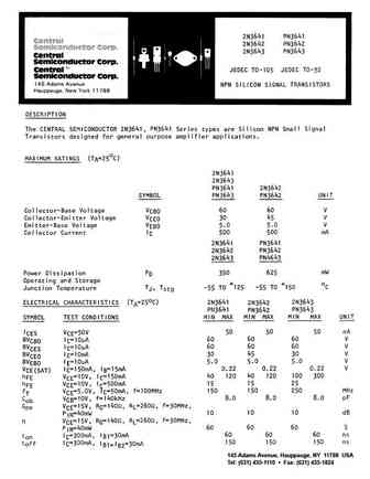
Type Designator: PN3642
Material of Transistor: Si
Polarity: NPN
Absolute Maximum Ratings
Maximum Collector Power Dissipation (Pc): 0.5 W
Maximum Collector-Base Voltage |Vcb|: 60 V
Maximum Collector-Emitter Voltage |Vce|: 45 V
Maximum Emitter-Base Voltage |Veb|: 5 V
Maximum Collector Current |Ic max|: 0.5 A
Max. Operating Junction Temperature (Tj): 150 °C
Electrical Characteristics
Transition Frequency (ft): 150 MHz
Collector Capacitance (Cc): 8 pF
Forward Current Transfer Ratio (hFE), MIN: 40
Package: TO92
PN3642 Substitution
- BJT ⓘ Cross-Reference Search
PN3642 datasheet
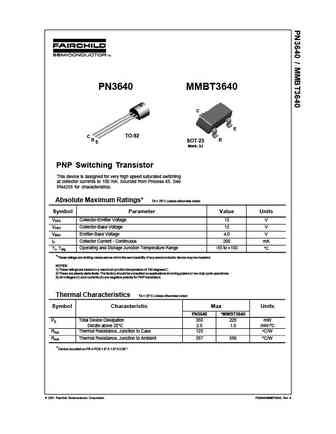
PN3642 NPN General Purpose Amplifier This device is designed for use as general purpose amplifiers and switches requiring collector currents to 300mA. TO-92 1 1. Emitter 2. Base 3. Collector Absolute Maximum Ratings* TA=25 C unless otherwise noted Symbol Parameter Value Units VCEO Collector-Emitter Voltage 45 V VCBO Collector-Base Voltage 60 V VEBO Emitter-Base Voltage 5.0 V I... See More ⇒
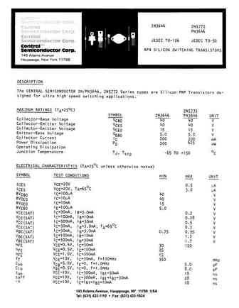
2n3641 2n3642 2n3643 pn3641 pn3642 pn3643.pdf ![]()
145 Adams Avenue, Hauppauge, NY 11788 USA Tel (631) 435-1110 Fax (631) 435-1824 ... See More ⇒
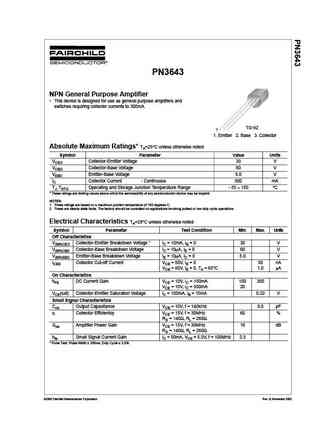
PN3643 NPN General Purpose Amplifier This device is designed for use as general purpose amplifiers and switches requiring collector currents to 300mA. TO-92 1 1. Emitter 2. Base 3. Collector Absolute Maximum Ratings* TA=25 C unless otherwise noted Symbol Parameter Value Units VCEO Collector-Emitter Voltage 30 V VCBO Collector-Base Voltage 60 V VEBO Emitter-Base Voltage 5.0 V I... See More ⇒
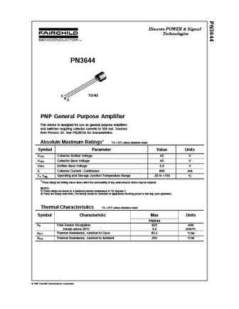
Discrete POWER & Signal Technologies PN3645 C TO-92 B E PNP General Purpose Amplifier This device is designed for use as general purpose amplifiers and switches requiring collector currents to 500 mA. Sourced from Process 63. See PN2907A for characteristics. Absolute Maximum Ratings* TA = 25 C unless otherwise noted Symbol Parameter Value Units V Collector-Emitter Voltage 60 V CEO... See More ⇒
Detailed specifications: PN3567, PN3568, PN3569, PN3638, PN3638A, PN3639, PN3640, PN3641, BC548, PN3643, PN3644, PN3645, PN3646, PN3691, PN3692, PN3693, PN3694
Keywords - PN3642 pdf specs
PN3642 cross reference
PN3642 equivalent finder
PN3642 pdf lookup
PN3642 substitution
PN3642 replacement
History: BCW46 | 2SB772-GR | PN3645 | BC846AWT1
🌐 : EN ES РУ
LIST
Last Update
BJT: GA1A4M | SBT42 | 2SA200-Y | 2SA200-O | 2SD882-Q | 2SD882-P
Popular searches
c711 transistor | k3599 transistor datasheet | 2sc1735 | transistor 2sc5200 | 2sb560 transistor | a1273 | c3421 transistor | c644 transistor

