TN3013 Datasheet. Specs and Replacement
Type Designator: TN3013 📄📄
Material of Transistor: Si
Polarity: NPN
Absolute Maximum Ratings
Maximum Collector Power Dissipation (Pc): 0.35 W
Maximum Collector-Base Voltage |Vcb|: 18 V
Maximum Collector-Emitter Voltage |Vce|: 18 V
Maximum Emitter-Base Voltage |Veb|: 5 V
Maximum Collector Current |Ic max|: 0.1 A
Max. Operating Junction Temperature (Tj): 150 °C
Electrical Characteristics
Transition Frequency (ft): 350 MHz
Collector Capacitance (Cc): 6 pF
Forward Current Transfer Ratio (hFE), MIN: 15
Package: TO92
TN3013 Substitution
- BJT ⓘ Cross-Reference Search
TN3013 datasheet
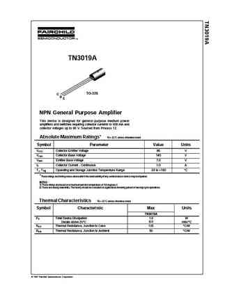
TN3019A TO-226 C B E NPN General Purpose Amplifier This device is designed for general purpose medium power amplifiers and switches requiring collector currents to 500 mA and collector voltages up to 80 V. Sourced from Process 12. Absolute Maximum Ratings* TA = 25 C unless otherwise noted Symbol Parameter Value Units VCEO Collector-Emitter Voltage 80 V VCBO Collector-Base Voltage 1... See More ⇒
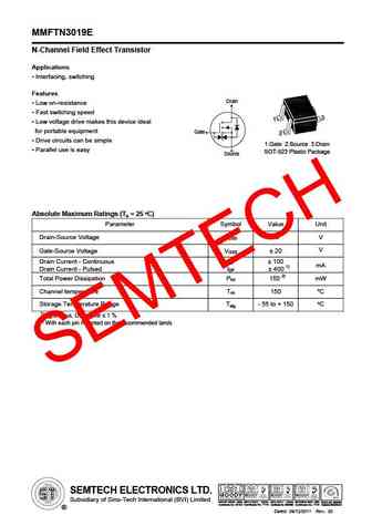
MMFTN3019E N-Channel Field Effect Transistor Applications Interfacing, switching Features Drain Low on-resistance Fast switching speed Low voltage drive makes this device ideal for portable equipment Gate Drive circuits can be simple Parallel use is easy Source O Absolute Maximum Ratings (Ta = 25 C) Parameter Symbol Value Unit Drain-Source Vo... See More ⇒
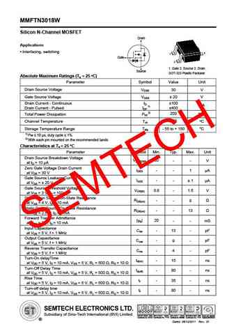
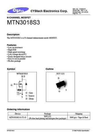
MMFTN3018W Silicon N-Channel MOSFET Drain Applications Interfacing, switching Gate 1. Gate 2. Source 3. Drain Source SOT-323 Plastic Package O Absolute Maximum Ratings (Ta = 25 C) Parameter Symbol Value Unit Drain Source Voltage VDSS 30 V Gate Source Voltage VGSS 20 V Drain Current - Continuous ID 100 mA Drain Current - Pulsed IDP 1) 400 200 mW Total Power ... See More ⇒
Detailed specifications: TN2907, TN2907A, TN2907AR, TN2907R, TN2923, TN2924, TN2925, TN2926, S8050, TN3019, TN3020, TN3053, TN3053A, TN3244, TN3245, TN3250, TN3250A
Keywords - TN3013 pdf specs
TN3013 cross reference
TN3013 equivalent finder
TN3013 pdf lookup
TN3013 substitution
TN3013 replacement
