TP3402 Specs and Replacement
Type Designator: TP3402
Material of Transistor: Si
Polarity: NPN
Absolute Maximum Ratings
Maximum Collector Power Dissipation (Pc): 0.56 W
Maximum Collector-Base Voltage |Vcb|: 25 V
Maximum Collector-Emitter Voltage |Vce|: 25 V
Maximum Emitter-Base Voltage |Veb|: 5 V
Maximum Collector Current |Ic max|: 0.5 A
Max. Operating Junction Temperature (Tj): 150 °C
Electrical Characteristics
Forward Current Transfer Ratio (hFE), MIN: 75
Package: TO92
TP3402 Substitution
- BJT ⓘ Cross-Reference Search
TP3402 datasheet
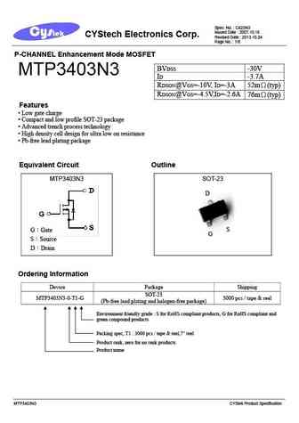
Spec. No. C422N3 Issued Date 2007.10.16 CYStech Electronics Corp. Revised Date 2013.10.24 Page No. 1/8 P-CHANNEL Enhancement Mode MOSFET BVDSS -30V MTP3403N3 ID -3.7A RDSON@VGS=-10V, ID=-3A 52m (typ) RDSON@VGS=-4.5V,ID=-2.6A 76m (typ) Features Low gate charge Compact and low profile SOT-23 package Advanced trench process technology High densit... See More ⇒
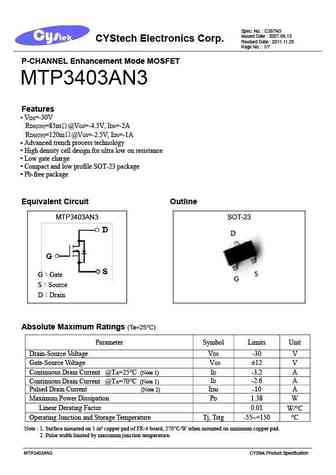
Spec. No. C387N3 Issued Date 2007.06.13 CYStech Electronics Corp. Revised Date 2011.11.29 Page No. 1/7 P-CHANNEL Enhancement Mode MOSFET MTP3403AN3 Features V =-30V DS @V =-4.5V, I =-2A R =85m GS DS DS(ON) @V =-2.5V, I =-1A R =120m GS DS DS(ON) Advanced trench process technology High density cell design for ultra low on resistance Low ... See More ⇒
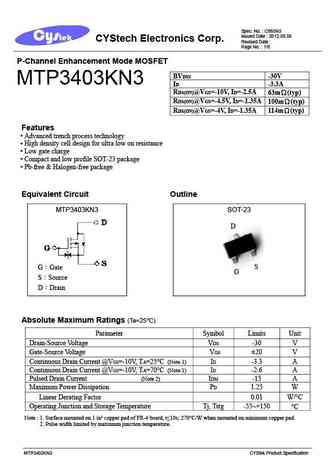
Spec. No. C865N3 Issued Date 2012.08.08 CYStech Electronics Corp. Revised Date Page No. 1/8 P-Channel Enhancement Mode MOSFET BVDSS -30V MTP3403KN3 ID -3.3A RDS(ON)@VGS=-10V, ID=-2.5A 63m (typ) RDS(ON)@VGS=-4.5V, ID=-1.35A 100m (typ) RDS(ON)@VGS=-4V, ID=-1.35A 114m (typ) Features Advanced trench process technology High density cell design for ultra low... See More ⇒
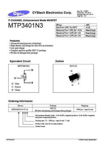
Spec. No. C388N3 Issued Date 2007.06.13 CYStech Electronics Corp. Revised Date 2017.06.19 Page No. 1/9 P-CHANNEL Enhancement Mode MOSFET BVDSS -30V MTP3401N3 ID@VGS=-10V, TA=25 C -4.2A RDS(ON)@VGS=-10V, ID=-4.2A 46m (typ) RDS(ON)@VGS=-4.5V, ID=-4A 51m (typ) RDS(ON)@VGS=-2.5V, ID=-1A 59m (typ) Features Advanced trench process technology High density c... See More ⇒
Detailed specifications: TP3391A, TP3392, TP3393, TP3394, TP3395, TP3396, TP3397, TP3398, 2SD2499, TP3403, TP3404, TP3405, TP3414, TP3415, TP3416, TP3417, TP3563
Keywords - TP3402 pdf specs
TP3402 cross reference
TP3402 equivalent finder
TP3402 pdf lookup
TP3402 substitution
TP3402 replacement
History: ZXTP08400BFF | 2SD1356R | 2N6076 | ZXTN5551Z | 2SC1486 | TP3053A | MD1124
🌐 : EN ES РУ

LIST
Last Update
BJT: GA1A4M | SBT42 | 2SA200-Y
Popular searches
s9015 transistor | irf540z | ss8550 transistor | irfp240 mosfet | tip141 | 2n404 | 2n4250 | d882 transistor equivalent