2N5959 Specs and Replacement
Type Designator: 2N5959
Material of Transistor: Si
Polarity: NPN
Absolute Maximum Ratings
Maximum Collector Power Dissipation (Pc): 100 W
Maximum Collector-Base Voltage |Vcb|: 100 V
Maximum Collector-Emitter Voltage |Vce|: 100 V
Maximum Emitter-Base Voltage |Veb|: 10 V
Maximum Collector Current |Ic max|: 20 A
Max. Operating Junction Temperature (Tj): 200 °C
Electrical Characteristics
Transition Frequency (ft): 10 MHz
Collector Capacitance (Cc): 350 pF
Forward Current Transfer Ratio (hFE), MIN: 30
Package: TO61
2N5959 Substitution
- BJT ⓘ Cross-Reference Search
2N5959 datasheet

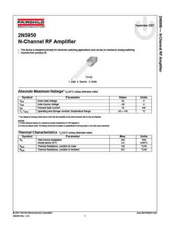
September 2007 2N5951 N-Channel RF Amplifier This device is designed primarily for electronic switching applications such as low on resistance analog switching. Sourced from process 50. TO-92 1 1. Gate 2. Source 3. Drain Absolute Maximum Ratings* Ta=25 C unless otherwise noted Symbol Parameter Value Units VDG Drain-Gate Voltage 30 V VGS Gate-Source Voltage -30 V IGF Forward... See More ⇒
September 2007 2N5950 N-Channel RF Amplifier This device is designed primarily for electronic switching applications such as low on resistance analog switching. Sourced from process 50. TO-92 1 1. Gate 2. Source 3. Drain Absolute Maximum Ratings* Ta=25 C unless otherwise noted Symbol Parameter Value Units VDG Drain-Gate Voltage 30 V VGS Gate-Source Voltage -30 V IGF Forward... See More ⇒
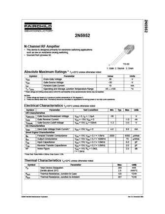
2N5952 N-Channel RF Ampifier This device is designed primarily for electronic switching applications such as low on resistance analog switching. Sourced from process 50. TO-92 1 1. Gate 2. Source 3. Drain Absolute Maximum Ratings * TC=25 C unless otherwise noted Symbol Parameter Value Units VDG Drain-Gate Voltage 30 V VGS Gate-Source Voltage -30 V IGF Forward Gate Current ... See More ⇒
2n5954 2n5955 2n5956 2n6372 2n6373 2n6374.pdf ![]()
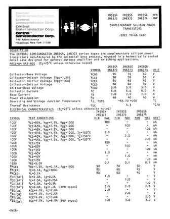
TM Central Semiconductor Corp. 145 Adams Avenue Hauppauge, NY 11788 USA Tel (631) 435-1110 Fax (631) 435-1824 www.centralsemi.com ... See More ⇒
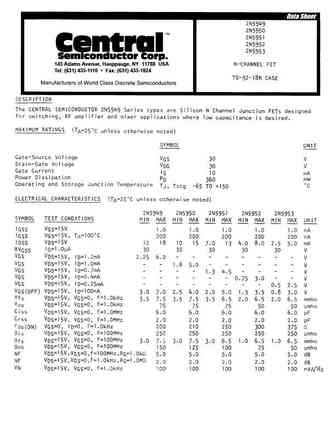
Detailed specifications: 2N5946, 2N5947, 2N595, 2N5954, 2N5955, 2N5956, 2N5957, 2N5958, BD135, 2N596, 2N5960, 2N5961, 2N5962, 2N5963, 2N5964, 2N5965, 2N5966
Keywords - 2N5959 pdf specs
2N5959 cross reference
2N5959 equivalent finder
2N5959 pdf lookup
2N5959 substitution
2N5959 replacement
🌐 : EN ES РУ

LIST
Last Update
BJT: GA1A4M | SBT42 | 2SA200-Y
Popular searches
2n2614 | 2sa777 replacement | 2sc828 transistor | 2sd357 | 110n8f6 mosfet datasheet | 2sc458 datasheet | irfz48 | bf494 transistor equivalent