2N6103 Specs and Replacement
Type Designator: 2N6103
Material of Transistor: Si
Polarity: NPN
Absolute Maximum Ratings
Maximum Collector Power Dissipation (Pc): 75 W
Maximum Collector-Base Voltage |Vcb|: 45 V
Maximum Collector-Emitter Voltage |Vce|: 40 V
Maximum Emitter-Base Voltage |Veb|: 5 V
Maximum Collector Current |Ic max|: 16 A
Max. Operating Junction Temperature (Tj): 150 °C
Electrical Characteristics
Transition Frequency (ft): 0.8 MHz
Forward Current Transfer Ratio (hFE), MIN: 15
Noise Figure, dB: -
Package: TO220
- BJT ⓘ Cross-Reference Search
2N6103 datasheet
..1. Size:99K jmnic
2n6102 2n6103.pdf 

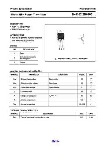
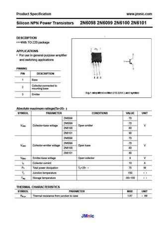
Product Specification www.jmnic.com Silicon NPN Power Transistors 2N6102 2N6103 DESCRIPTION With TO-220 package 2N6102 with short pin APPLICATIONS For use in general-purpose amplifier and switching applications PINNING PIN DESCRIPTION 1 Base Collector;connected to 2 mounting base 3 Emitter Absolute maximum ratings(Ta=25 ) SYMBOL PARAMETER CONDITIONS VALUE ... See More ⇒
..2. Size:195K inchange semiconductor
2n6103.pdf 
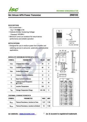
isc Silicon NPN Power Transistor 2N6103 DESCRIPTION DC Current Gain - h = 15-60@ I = 8A FE C Collector-Emitter Sustaining Voltage- V = 40V(Min) CEO(SUS) Minimum Lot-to-Lot variations for robust device performance and reliable operation APPLICATIONS Designed for use in medium power liner amplifier and switching service in consumer ,automotive and industrial applications.... See More ⇒
..3. Size:57K inchange semiconductor
2n6102 2n6103.pdf 
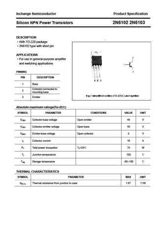
Inchange Semiconductor Product Specification Silicon NPN Power Transistors 2N6102 2N6103 DESCRIPTION With TO-220 package 2N6102 type with short pin APPLICATIONS For use in general-purpose amplifier and switching applications PINNING PIN DESCRIPTION 1 Base Collector;connected to 2 mounting base 3 Emitter Absolute maximum ratings(Ta=25 ) SYMBOL PARAMETER CON... See More ⇒
9.1. Size:149K motorola
2n6107 2n6111 2n6288 2n6109 2n6292.pdf 

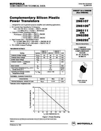
Order this document MOTOROLA by 2N6107/D SEMICONDUCTOR TECHNICAL DATA 2N6057 thru 2N6059 (See 2N6050) Complementary Silicon Plastic PNP Power Transistors 2N6107 . . . designed for use in general purpose amplifier and switching applications. 2N6109* DC Current Gain Specified to 7.0 Amperes hFE = 30 150 @ IC = 3.0 Adc 2N6111, 2N6288 hFE = 2.3 (Min) @ IC = 7.0 Adc All ... See More ⇒
9.2. Size:48K st
2n6107 2n6111.pdf 

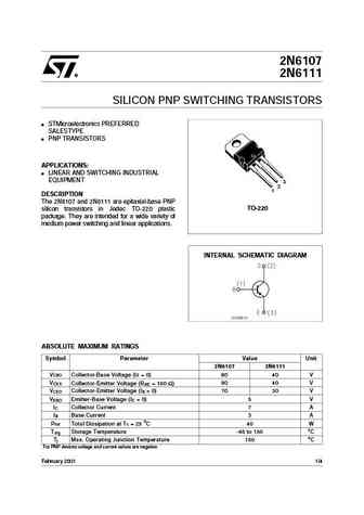
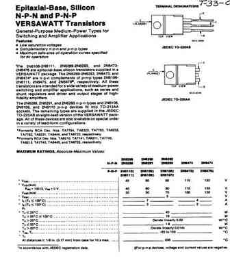
2N6107 2N6111 SILICON PNP SWITCHING TRANSISTORS STMicroelectronics PREFERRED SALESTYPE PNP TRANSISTORS APPLICATIONS LINEAR AND SWITCHING INDUSTRIAL EQUIPMENT 3 2 1 DESCRIPTION The 2N6107 and 2N6111 are epitaxial-base PNP TO-220 silicon transistors in Jedec TO-220 plastic package. They are intended for a wide variety of medium power switching and linear applications... See More ⇒
9.4. Size:241K onsemi
2n6107g 2n6109g 2n6111g 2n6288g 2n6292g.pdf 

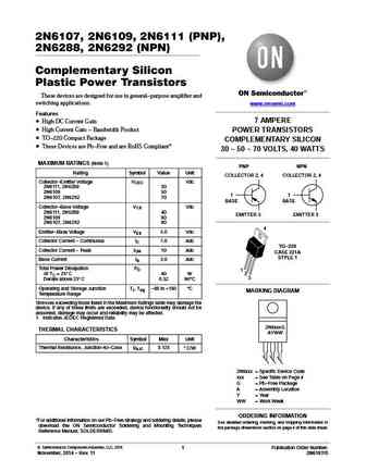
2N6107, 2N6109, 2N6111 (PNP), 2N6288, 2N6292 (NPN) Complementary Silicon Plastic Power Transistors These devices are designed for use in general-purpose amplifier and switching applications. www.onsemi.com Features 7 AMPERE High DC Current Gain High Current Gain - Bandwidth Product POWER TRANSISTORS TO-220 Compact Package COMPLEMENTARY SILICON These Devices are Pb-... See More ⇒
9.5. Size:102K onsemi
2n6109g 2n6109g 2n6107g.pdf 

2N6107, 2N6109, 2N6111 (PNP), 2N6288, 2N6292 (NPN) Complementary Silicon Plastic Power Transistors These devices are designed for use in general-purpose amplifier and switching applications. www.onsemi.com Features 7 AMPERE High DC Current Gain High Current Gain - Bandwidth Product POWER TRANSISTORS TO-220 Compact Package COMPLEMENTARY SILICON These Devices are Pb-... See More ⇒
9.6. Size:241K onsemi
2n6107 2n6109 2n6111 2n6288 2n6292.pdf 

2N6107, 2N6109, 2N6111 (PNP), 2N6288, 2N6292 (NPN) Complementary Silicon Plastic Power Transistors These devices are designed for use in general-purpose amplifier and switching applications. www.onsemi.com Features 7 AMPERE High DC Current Gain High Current Gain - Bandwidth Product POWER TRANSISTORS TO-220 Compact Package COMPLEMENTARY SILICON These Devices are Pb-... See More ⇒
9.7. Size:102K onsemi
2n6107g.pdf 

2N6107, 2N6109, 2N6111 (PNP), 2N6288, 2N6292 (NPN) Complementary Silicon Plastic Power Transistors These devices are designed for use in general-purpose amplifier and switching applications. www.onsemi.com Features 7 AMPERE High DC Current Gain High Current Gain - Bandwidth Product POWER TRANSISTORS TO-220 Compact Package COMPLEMENTARY SILICON These Devices are Pb-... See More ⇒
9.9. Size:95K cdil
2n6107 2n6292.pdf 

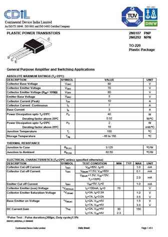
Continental Device India Limited An ISO/TS 16949, ISO 9001 and ISO 14001 Certified Company PLASTIC POWER TRANSISTORS 2N6107 PNP 2N6292 NPN TO-220 Plastic Package General Purpose Amplifier and Switching Applications ABSOLUTE MAXIMUM RATINGS (Ta=25 C) DESCRIPTION SYMBOL VALUE UNIT VCBO Collector Base Voltage 80 V Collector Emitter Voltage VCEO 70 V Collector Emitter Voltage (RBE= 100... See More ⇒
9.10. Size:315K cdil
2n6101.pdf 

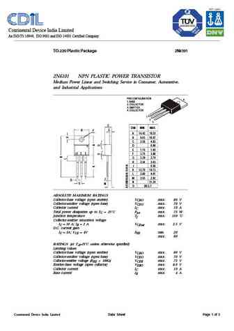
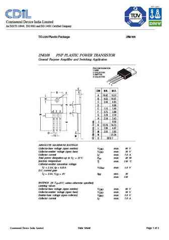
Continental Device India Limited An ISO/TS 16949, ISO 9001 and ISO 14001 Certified Company TO-220 Plastic Package 2N6101 2N6101 NPN PLASTIC POWER TRANSISTOR Medium Power Linear and Switching Service in Consumer, Automotive, and Industrial Applications PIN CONFIGURATION 4 1. BASE 2. COLLECTOR 3. EMITTER 4. COLLECTOR 1 2 3 C DIM MIN. MAX. B E F A 14.42 16.51 B 9.63 10.67 C 3.... See More ⇒
9.11. Size:249K cdil
2n6109.pdf 

Continental Device India Limited An ISO/TS 16949, ISO 9001 and ISO 14001 Certified Company TO-220 Plastic Package 2N6109 2N6109 PNP PLASTIC POWER TRANSISTOR General Purpose Amplifier and Switching Application PIN CONFIGURATION 4 1. BASE 2. COLLECTOR 3. EMITTER 4. COLLECTOR 1 2 3 C DIM MIN. MAX. E B F A 14.42 16.51 B 9.63 10.67 C 3.56 4.83 D0.90 E 1.15 1.40 1 2 3 F 3.75 ... See More ⇒
9.12. Size:106K jmnic
2n6098 2n6099 2n6100 2n6101.pdf 

Product Specification www.jmnic.com Silicon NPN Power Transistors 2N6098 2N6099 2N6100 2N6101 DESCRIPTION With TO-220 package APPLICATIONS For use in general-purpose amplifier and switching applications PINNING PIN DESCRIPTION 1 Base Collector;connected to 2 mounting base 3 Emitter Absolute maximum ratings(Ta=25 ) SYMBOL PARAMETER CONDITIONS VALUE UNIT 2N... See More ⇒
9.13. Size:198K inchange semiconductor
2n6107.pdf 
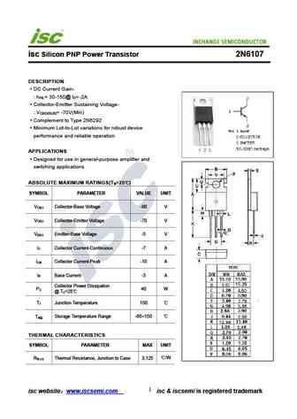
INCHANGE Semiconductor isc Silicon PNP Power Transistor 2N6107 DESCRIPTION DC Current Gain- h = 30-150@ I = -2A FE C Collector-Emitter Sustaining Voltage- V = -70V(Min) CEO(SUS) Complement to Type 2N6292 Minimum Lot-to-Lot variations for robust device performance and reliable operation APPLICATIONS Designed for use in general-purpose amplifier and switching applicati... See More ⇒
9.14. Size:119K inchange semiconductor
2n6098 2n6099 2n6100 2n6101.pdf 
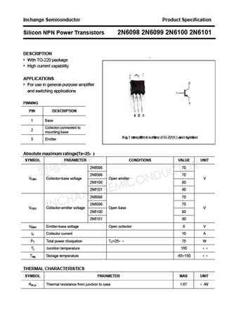
Inchange Semiconductor Product Specification Silicon NPN Power Transistors 2N6098 2N6099 2N6100 2N6101 DESCRIPTION With TO-220 package High current capability APPLICATIONS For use in general-purpose amplifier and switching applications PINNING PIN DESCRIPTION 1 Base Collector;connected to 2 mounting base 3 Emitter Absolute maximum ratings(Ta=25 ) SYMBOL PA... See More ⇒
9.15. Size:197K inchange semiconductor
2n6106.pdf 
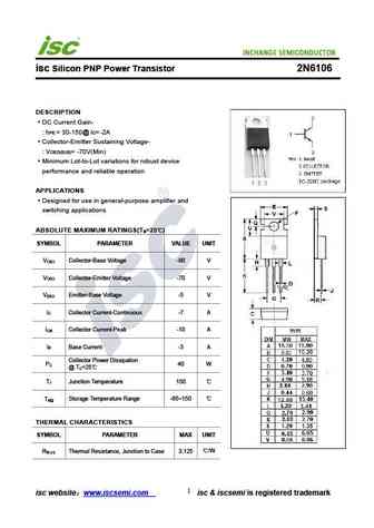
INCHANGE Semiconductor isc Silicon PNP Power Transistor 2N6106 DESCRIPTION DC Current Gain- h = 30-150@ I = -2A FE C Collector-Emitter Sustaining Voltage- V = -70V(Min) CEO(SUS) Minimum Lot-to-Lot variations for robust device performance and reliable operation APPLICATIONS Designed for use in general-purpose amplifier and switching applications ABSOLUTE MAXIMUM RATINGS... See More ⇒
9.16. Size:121K inchange semiconductor
2n6106 2n6108 2n6110.pdf 
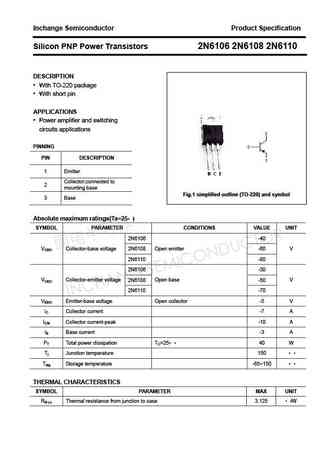
Inchange Semiconductor Product Specification Silicon PNP Power Transistors 2N6106 2N6108 2N6110 DESCRIPTION With TO-220 package With short pin APPLICATIONS Power amplifier and switching circuits applications PINNING PIN DESCRIPTION 1 Emitter Collector;connected to 2 mounting base Fig.1 simplified outline (TO-220) and symbol 3 Base Absolute maximum ratings(Ta=2... See More ⇒
9.17. Size:195K inchange semiconductor
2n6101.pdf 

isc Silicon NPN Power Transistor 2N6101 DESCRIPTION DC Current Gain - h = 20-80@ I = 5A FE C Collector-Emitter Sustaining Voltage- V = 70V(Min) CEO(SUS) Minimum Lot-to-Lot variations for robust device performance and reliable operation APPLICATIONS Designed for use in medium power liner amplifier and switching service in consumer ,automotive and industrial applications.... See More ⇒
9.18. Size:191K inchange semiconductor
2n6108.pdf 
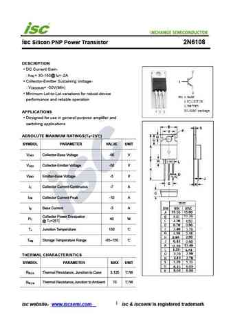
isc Silicon PNP Power Transistor 2N6108 DESCRIPTION DC Current Gain- h = 30-150@ I = -2A FE C Collector-Emitter Sustaining Voltage- V = -50V(Min) CEO(SUS) Minimum Lot-to-Lot variations for robust device performance and reliable operation APPLICATIONS Designed for use in general-purpose amplifier and switching applications ABSOLUTE MAXIMUM RATINGS(T =25 ) a SYMBOL PA... See More ⇒
9.19. Size:197K inchange semiconductor
2n6109.pdf 
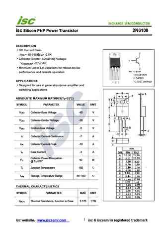
INCHANGE Semiconductor isc Silicon PNP Power Transistor 2N6109 DESCRIPTION DC Current Gain- h = 30-150@ I = -2.5A FE C Collector-Emitter Sustaining Voltage- V = -50V(Min) CEO(SUS) Minimum Lot-to-Lot variations for robust device performance and reliable operation APPLICATIONS Designed for use in general-purpose amplifier and switching applications ABSOLUTE MAXIMUM RATIN... See More ⇒
9.20. Size:121K inchange semiconductor
2n6107 2n6109 2n6111.pdf 
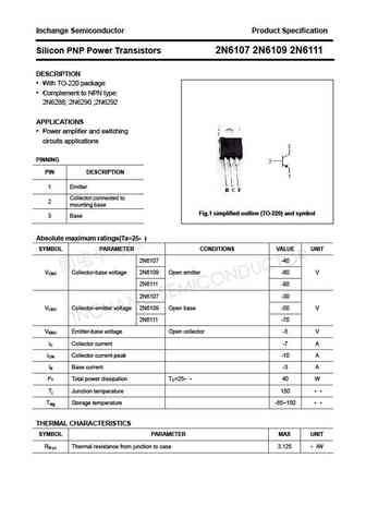
Inchange Semiconductor Product Specification Silicon PNP Power Transistors 2N6107 2N6109 2N6111 DESCRIPTION With TO-220 package Complement to NPN type 2N6288; 2N6290 ;2N6292 APPLICATIONS Power amplifier and switching circuits applications PINNING PIN DESCRIPTION 1 Emitter Collector;connected to 2 mounting base Fig.1 simplified outline (TO-220) and symbol 3 B... See More ⇒
9.21. Size:187K inchange semiconductor
2n6102.pdf 
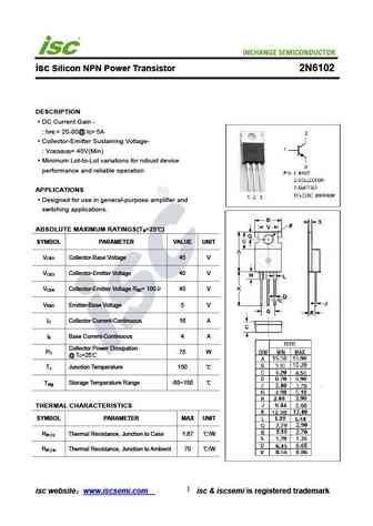
isc Silicon NPN Power Transistor 2N6102 DESCRIPTION DC Current Gain - h = 20-80@ I = 5A FE C Collector-Emitter Sustaining Voltage- V = 40V(Min) CEO(SUS) Minimum Lot-to-Lot variations for robust device performance and reliable operation APPLICATIONS Designed for use in general-purpose amplifier and switching applications. ABSOLUTE MAXIMUM RATINGS(T =25 ) a SYMBOL PAR... See More ⇒
9.22. Size:188K inchange semiconductor
2n6100.pdf 
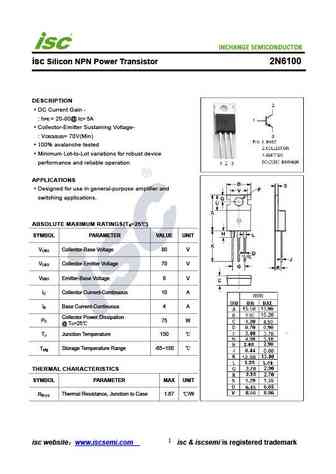
isc Silicon NPN Power Transistor 2N6100 DESCRIPTION DC Current Gain - h = 20-80@ I = 5A FE C Collector-Emitter Sustaining Voltage- V = 70V(Min) CEO(SUS) 100% avalanche tested Minimum Lot-to-Lot variations for robust device performance and reliable operation APPLICATIONS Designed for use in general-purpose amplifier and switching applications. ABSOLUTE MAXIMUM RATINGS... See More ⇒
Detailed specifications: 2N60A, 2N60B, 2N60C, 2N61, 2N610, 2N6100, 2N6101, 2N6102, BD139, 2N6104, 2N6105, 2N6106, 2N6107, 2N6108, 2N6109, 2N611, 2N6110
Keywords - 2N6103 pdf specs
2N6103 cross reference
2N6103 equivalent finder
2N6103 pdf lookup
2N6103 substitution
2N6103 replacement
![]()
