2SC5516 Datasheet. Specs and Replacement
Type Designator: 2SC5516 📄📄
Material of Transistor: Si
Polarity: NPN
Absolute Maximum Ratings
Maximum Collector Power Dissipation (Pc): 70 W
Maximum Collector-Base Voltage |Vcb|: 1500 V
Maximum Collector-Emitter Voltage |Vce|: 600 V
Maximum Emitter-Base Voltage |Veb|: 5 V
Maximum Collector Current |Ic max|: 20 A
Max. Operating Junction Temperature (Tj): 150 °C
Electrical Characteristics
Transition Frequency (ft): 3 MHz
Forward Current Transfer Ratio (hFE), MIN: 5
Noise Figure, dB: -
Package: TOP-3E
- BJT ⓘ Cross-Reference Search
2SC5516 datasheet
..1. Size:35K panasonic
2sc5516.pdf 

Power Transistors 2SC5516 Silicon NPN triple diffusion mesa type For horizontal deflection output Unit mm 15.5 0.5 3.0 0.3 3.2 0.1 Features 5 5 High breakdown voltage, and high reliability through the use of a glass passivation layer High-speed switching 5 Wide area of safe operation (ASO) 5 4.0 5 2.0 0.2 1.1 0.1 Absolute Maximum Ratings (TC=25 C) 0.... See More ⇒
..2. Size:187K inchange semiconductor
2sc5516.pdf 
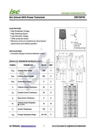
INCHANGE Semiconductor isc Silicon NPN Power Transistor 2SC5516 DESCRIPTION High Breakdown Voltage High Switching Speed Low Saturation Voltage 100% avalanche tested Minimum Lot-to-Lot variations for robust device performance and reliable operation APPLICATIONS Character display horizontal deflection output ABSOLUTE MAXIMUM RATINGS(T =25 ) a SYMBOL PARAMETER VALUE UNIT... See More ⇒
8.1. Size:51K rohm
2sc5511.pdf 

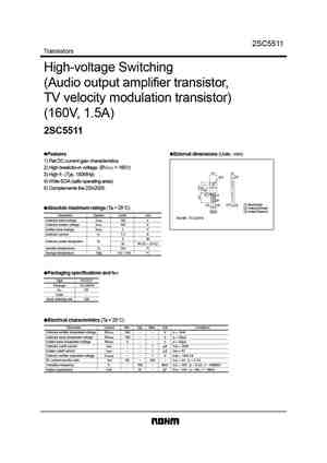
2SC5511 Transistors High-voltage Switching (Audio output amplifier transistor, TV velocity modulation transistor) (160V, 1.5A) 2SC5511 Features External dimensions (Units mm) 1) Flat DC current gain characteristics. 2) High breakdown voltage. (BVCEO = 160V) 10.0 4.5 3) High fT. (Typ. 150MHz) 3.2 2.8 4) Wide SOA (safe operating area). 5) Complements the 2SA2005. 1.2 1.3 ... See More ⇒
8.2. Size:35K panasonic
2sc5514.pdf 

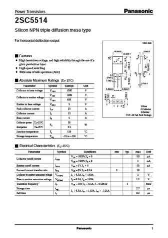
Power Transistors 2SC5514 Silicon NPN triple diffusion mesa type For horizontal deflection output Unit mm 15.5 0.5 3.0 0.3 3.2 0.1 Features 5 5 High breakdown voltage, and high reliability through the use of a glass passivation layer High-speed switching 5 Wide area of safe operation (ASO) 5 4.0 5 2.0 0.2 1.1 0.1 Absolute Maximum Ratings (TC=25 C) 0.... See More ⇒
8.3. Size:35K panasonic
2sc5515.pdf 

Power Transistors 2SC5515 Silicon NPN triple diffusion mesa type For horizontal deflection output Unit mm 15.5 0.5 3.0 0.3 3.2 0.1 Features 5 5 High breakdown voltage, and high reliability through the use of a glass passivation layer High-speed switching 5 Wide area of safe operation (ASO) 5 4.0 5 2.0 0.2 1.1 0.1 Absolute Maximum Ratings (TC=25 C) 0.... See More ⇒
8.4. Size:47K panasonic
2sc5519.pdf 

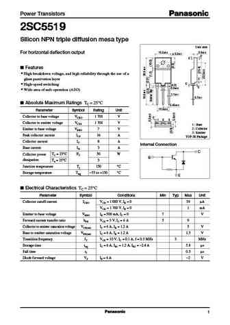
Power Transistors 2SC5519 2SC5519 2SC5519 2SC5519 2SC5519 Silicon NPN triple diffusion mesa type Unit mm 15.5 0.5 3.0 0.3 For horizontal deflection output 3.2 0.1 5 5 Features High breakdown voltage, and high reliability through the use of a 5 glass passivation layer 5 High-speed switching (4.0) 5 2.0 0.2 Wide area of safe operation (ASO) 1.... See More ⇒
8.5. Size:35K panasonic
2sc5513.pdf 

Power Transistors 2SC5513 Silicon NPN triple diffusion mesa type For horizontal deflection output Unit mm 15.5 0.5 3.0 0.3 3.2 0.1 Features 5 5 High breakdown voltage, and high reliability through the use of a glass passivation layer High-speed switching 5 Wide area of safe operation (ASO) 5 4.0 5 2.0 0.2 1.1 0.1 Absolute Maximum Ratings (TC=25 C) 0.... See More ⇒
8.6. Size:35K panasonic
2sc5518.pdf 

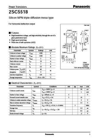
Power Transistors 2SC5518 Silicon NPN triple diffusion mesa type For horizontal deflection output Unit mm 15.5 0.5 3.0 0.3 3.2 0.1 Features 5 5 High breakdown voltage, and high reliability through the use of a glass passivation layer High-speed switching 5 Wide area of safe operation (ASO) 5 4.0 5 2.0 0.2 1.1 0.1 Absolute Maximum Ratings (TC=25 C) 0.... See More ⇒
8.7. Size:35K panasonic
2sc5517.pdf 

Power Transistors 2SC5517 Silicon NPN triple diffusion mesa type For horizontal deflection output Unit mm 15.5 0.5 3.0 0.3 3.2 0.1 Features 5 5 High breakdown voltage, and high reliability through the use of a glass passivation layer High-speed switching 5 Wide area of safe operation (ASO) 5 4.0 5 2.0 0.2 1.1 0.1 Absolute Maximum Ratings (TC=25 C) 0.... See More ⇒
8.8. Size:179K inchange semiconductor
2sc5517.pdf 
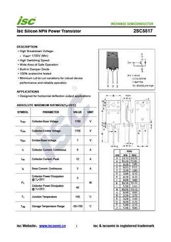
INCHANGE Semiconductor isc Silicon NPN Power Transistor 2SC5517 DESCRIPTION High Breakdown Voltage- V = 1700V (Min) CBO High Switching Speed Wide Area of Safe Operation Built-in Damper Diode 100% avalanche tested Minimum Lot-to-Lot variations for robust device performance and reliable operation APPLICATIONS Designed for horizontal deflection output applications AB... See More ⇒
Detailed specifications: 2SC5505, 2SC5506, 2SC5507, 2SC5508, 2SC5509, 2SC5513, 2SC5514, 2SC5515, TIP2955, 2SC5517, 2SC5518, 2SC5519, 2SC5534, 2SC5536, 2SC5537, 2SC5538, 2SC5539
Keywords - 2SC5516 pdf specs
2SC5516 cross reference
2SC5516 equivalent finder
2SC5516 pdf lookup
2SC5516 substitution
2SC5516 replacement

