STD129 Datasheet. Specs and Replacement
Type Designator: STD129
Material of Transistor: Si
Polarity: NPN
Absolute Maximum Ratings
Maximum Collector Power Dissipation (Pc): 0.625 W
Maximum Collector-Base Voltage |Vcb|: 40 V
Maximum Collector-Emitter Voltage |Vce|: 15 V
Maximum Emitter-Base Voltage |Veb|: 7 V
Maximum Collector Current |Ic max|: 5 A
Max. Operating Junction Temperature (Tj): 150 °C
Electrical Characteristics
Transition Frequency (ft): 150 MHz
Collector Capacitance (Cc): 50 pF
Forward Current Transfer Ratio (hFE), MIN: 160
Noise Figure, dB: -
Package: TO-92
- BJT ⓘ Cross-Reference Search
STD129 datasheet
..1. Size:53K auk
std129.pdf 

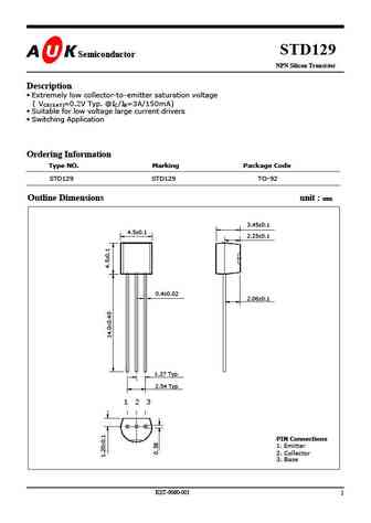
STD129 Semiconductor Semiconductor NPN Silicon Transistor Description Extremely low collector-to-emitter saturation voltage ( VCE(SAT)=0.2V Typ. @IC/IB=3A/150mA) Suitable for low voltage large current drivers Switching Application Ordering Information Type NO. Marking Package Code STD129 STD129 TO-92 Outline Dimensions unit mm 3.45 0.1 4.5 0.1 2.25... See More ⇒
9.3. Size:321K st
std12nf06l.pdf 

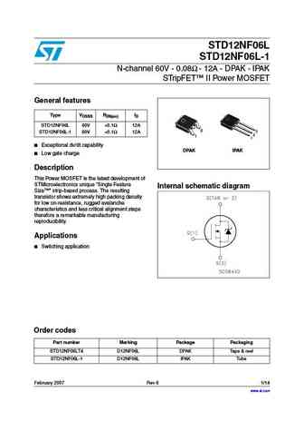
STD12NF06L STD12NF06L-1 N-channel 60V - 0.08 - 12A - DPAK - IPAK STripFET II Power MOSFET General features VDSSS RDS(on) ID Type STD12NF06L 60V ... See More ⇒
9.4. Size:176K st
std12n.pdf 

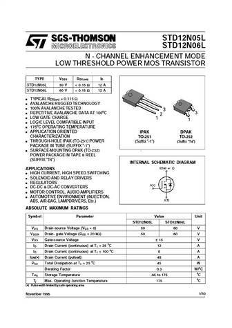
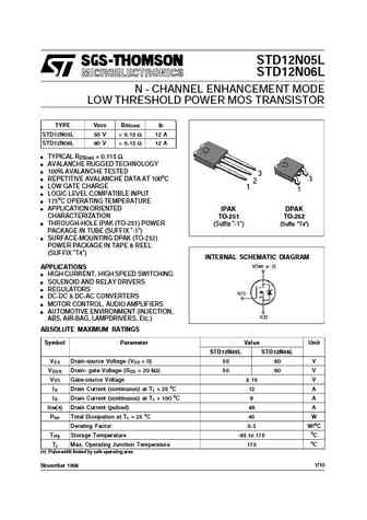
STD12N05L STD12N06L N - CHANNEL ENHANCEMENT MODE LOW THRESHOLD POWER MOS TRANSISTOR TYPE V R I DSS DS(on) D STD12N05L 50 V ... See More ⇒
9.5. Size:581K st
std12nm50n stf12nm50n sti12nm50n stp12nm50n.pdf 

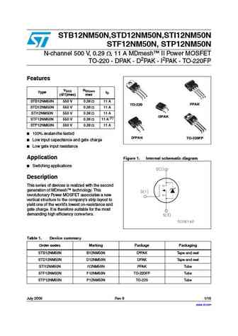
STB12NM50N,STD12NM50N,STI12NM50N STF12NM50N, STP12NM50N N-channel 500 V, 0.29 , 11 A MDmesh II Power MOSFET TO-220 - DPAK - D2PAK - I2PAK - TO-220FP Features VDSS RDS(on) Type ID (@Tjmax) max 3 3 2 2 1 1 STB12NM50N 550 V 0.38 11 A I PAK TO-220 STD12NM50N 550 V 0.38 11 A 3 1 STI12NM50N 550 V 0.38 11 A DPAK STF12NM50N 550 V 0.38 11 A (1) STP12NM50N 5... See More ⇒
9.6. Size:1091K st
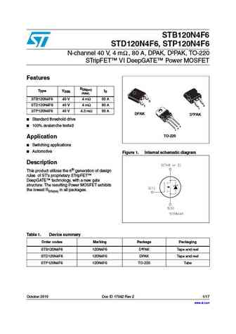
stb120n4f6 std120n4f6.pdf 

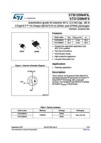
STB120N4F6, STD120N4F6 Automotive-grade N-channel 40 V, 3.5 m typ., 80 A STripFET F6 Power MOSFETs in DPAK and D PAK packages Datasheet - production data Features Order codes VDS RDS(on) max. ID STB120N4F6 40 V 4 m 80 A TAB STD120N4F6 40 V 4 m 80 A TAB Designed for automotive applications and 3 3 AEC-Q101 qualified 1 1 Very low on-resistance DPAK D PAK ... See More ⇒
9.7. Size:632K st
std127dt4.pdf 

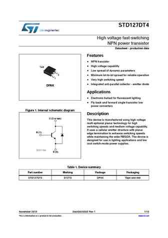
STD127DT4 High voltage fast-switching NPN power transistor Datasheet - production data Features NPN transistor High voltage capability TAB Low spread of dynamic parameters 3 Minimum lot-to-lot spread for reliable operation 1 Very high switching speed Integrated anti-parallel collector - emitter diode DPAK Applications Electronic ballast for fluoresce... See More ⇒
9.8. Size:586K st
stb12nm50n std12nm50n sti12nm50n stf12nm50n stp12nm50n.pdf 

STB12NM50N,STD12NM50N,STI12NM50N STF12NM50N, STP12NM50N N-channel 500 V, 0.29 , 11 A MDmesh II Power MOSFET TO-220 - DPAK - D2PAK - I2PAK - TO-220FP Features VDSS RDS(on) Type ID (@Tjmax) max 3 3 2 2 1 1 STB12NM50N 550 V 0.38 11 A I PAK TO-220 STD12NM50N 550 V 0.38 11 A 3 1 STI12NM50N 550 V 0.38 11 A DPAK STF12NM50N 550 V 0.38 11 A (1) STP12NM50N 5... See More ⇒
9.9. Size:539K st
std12n60dm2ag.pdf 

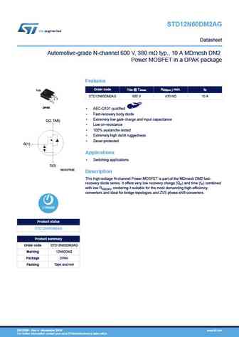
STD12N60DM2AG Datasheet Automotive-grade N-channel 600 V, 380 m typ., 10 A MDmesh DM2 Power MOSFET in a DPAK package Features VDS @ TJmax RDS(on ) max. ID Order code TAB STD12N60DM2AG 650 V 430 m 10 A 3 2 1 DPAK AEC-Q101 qualified Fast-recovery body diode Extremely low gate charge and input capacitance D(2, TAB) Low on-resistance 100% avalanche test... See More ⇒
9.10. Size:1025K st
stb12nm50nd std12nm50nd stf12nm50nd.pdf 

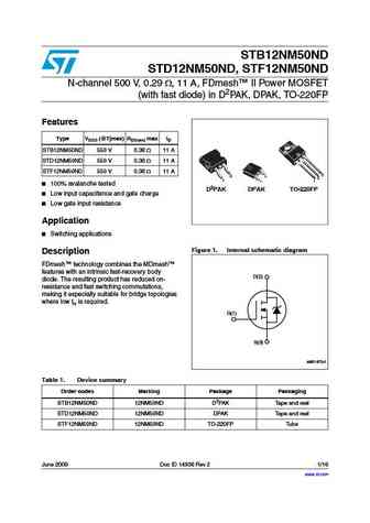
STB12NM50ND STD12NM50ND, STF12NM50ND N-channel 500 V, 0.29 , 11 A, FDmesh II Power MOSFET (with fast diode) in D2PAK, DPAK, TO-220FP Features Type VDSS (@Tjmax) RDS(on) max ID STB12NM50ND 550 V 0.38 11 A STD12NM50ND 550 V 0.38 11 A STF12NM50ND 550 V 0.38 11 A 3 3 3 2 1 1 1 100% avalanche tested D2PAK DPAK TO-220FP Low input capacitance and gate charge ... See More ⇒
9.11. Size:81K st
std12ne06l.pdf 

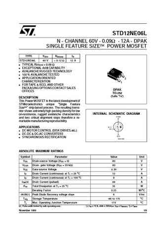
STD12NE06L N - CHANNEL 60V - 0.09 - 12A - DPAK SINGLE FEATURE SIZE POWER MOSFET TYPE VDSS RDS(on) ID STD12NE06L 60 V ... See More ⇒
9.12. Size:443K st
std12nf06.pdf 

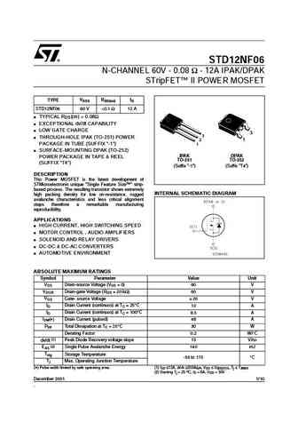
STD12NF06 N-CHANNEL 60V - 0.08 - 12A IPAK/DPAK STripFET II POWER MOSFET TYPE VDSS RDS(on) ID STD12NF06 60 V ... See More ⇒
9.13. Size:333K st
std12nf06-1.pdf 

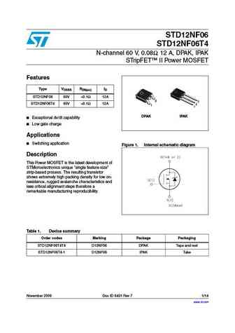
STD12NF06 STD12NF06T4 N-channel 60 V, 0.08 , 12 A, DPAK, IPAK STripFET II Power MOSFET Features VDSSS RDS(on) ID Type STD12NF06 60V ... See More ⇒
9.14. Size:935K st
std12n65m2.pdf 

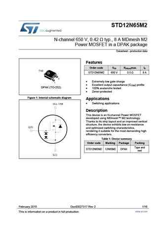
STD12N65M2 N-channel 650 V, 0.42 typ., 8 A MDmesh M2 Power MOSFET in a DPAK package Datasheet - production data Features Order code V R max. I DS DS(on) D STD12N65M2 650 V 0.5 8 A Extremely low gate charge Excellent output capacitance (COSS) profile DPAK (TO-252) 100% avalanche tested Zener-protected Figure 1 Internal schematic diagram Applicatio... See More ⇒
9.15. Size:106K st
std12ne06.pdf 

STD12NE06 N - CHANNEL 60V - 0.08 - 12A - DPAK SINGLE FEATURE SIZE POWER MOSFET TYPE VDSS RDS(on) ID STD12NE06 60 V ... See More ⇒
9.16. Size:303K st
std12nf06l std12nf06l-1.pdf 

STD12NF06L STD12NF06L-1 N-channel 60V - 0.08 - 12A - DPAK - IPAK STripFET II Power MOSFET General features VDSSS RDS(on) ID Type STD12NF06L 60V ... See More ⇒
9.17. Size:748K st
std12n50m2.pdf 

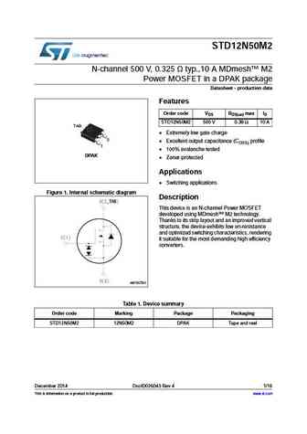
STD12N50M2 N-channel 500 V, 0.325 typ.,10 A MDmesh M2 Power MOSFET in a DPAK package Datasheet - production data Features Order code VDS RDS(on) max ID STD12N50M2 500 V 0.38 10 A TAB Extremely low gate charge 3 Excellent output capacitance (COSS) profile 1 100% avalanche tested DPAK Zener-protected Applications Switching applications Figure 1. Int... See More ⇒
9.18. Size:1040K st
std12n65m5 stf12n65m5 sti12n65m5 stp12n65m5 stu12n65m5.pdf 

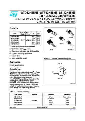
STD12N65M5, STF12N65M5, STI12N65M5 STP12N65M5, STU12N65M5 N-channel 650 V, 0.39 , 8.5 A MDmesh V Power MOSFET DPAK, I2PAK, TO-220FP, TO-220, IPAK Features VDSS @ RDS(on) Type ID PTOT 3 TJmax max 2 3 1 2 1 STD12N65M5 8.5 A 70 W IPAK TO-220 STF12N65M5 8.5 A(1) 25 W 3 STI12N65M5 710 V ... See More ⇒
9.19. Size:335K st
std12nf06 std12nf06t4.pdf 

STD12NF06 STD12NF06T4 N-channel 60 V, 0.08 , 12 A, DPAK, IPAK STripFET II Power MOSFET Features VDSSS RDS(on) ID Type STD12NF06 60V ... See More ⇒
9.20. Size:316K st
std12nf06l-1 std12nf06lt4.pdf 

STD12NF06L STD12NF06L-1 N-channel 60V - 0.08 - 12A - DPAK - IPAK STripFET II Power MOSFET General features VDSSS RDS(on) ID Type STD12NF06L 60V ... See More ⇒
9.22. Size:177K st
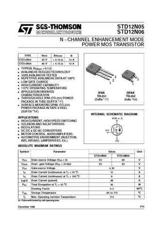
std12n05.pdf 

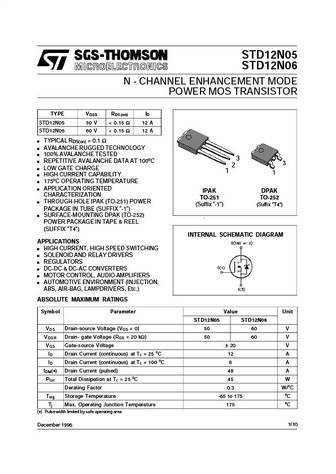
STD12N05 STD12N06 N - CHANNEL ENHANCEMENT MODE POWER MOS TRANSISTOR TYPE V R I DSS DS(on) D STD12N05 50 V ... See More ⇒
9.23. Size:806K st
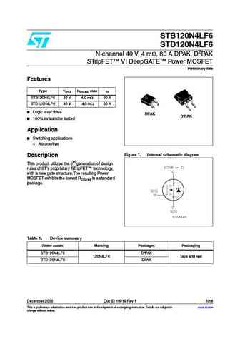
stb120n4lf6 std120n4lf6.pdf 

STB120N4LF6 STD120N4LF6 N-channel 40 V, 4 m , 80 A DPAK, D2PAK STripFET VI DeepGATE Power MOSFET Preliminary data Features Type VDSS RDS(on) max ID STB120N4LF6 40 V 4.0 m 80 A STD120N4LF6 40 V 4.0 m 80 A 3 3 1 1 Logic level drive DPAK D PAK 100% avalanche tested Application Switching applications Automotive Figure 1. Internal schematic diagram... See More ⇒
9.24. Size:324K auk
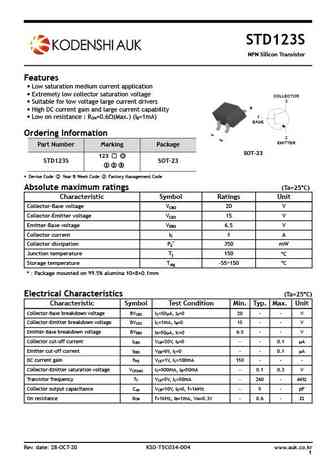
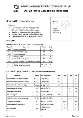
std123s.pdf 

STD123S NPN Silicon Transistor Features Low saturation medium current application Extremely low collector saturation voltage COLLECTOR 3 Suitable for low voltage large current drivers 3 High DC current gain and large current capability 1 Low on resistance R =0.6 (Max.) (I =1mA) ON B BASE Ordering Information 2 EMITTER Part Number Marking P... See More ⇒
9.25. Size:148K auk
std123uf.pdf 

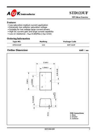
STD123UF Semiconductor Semiconductor NPN Silicon Transistor Features Low saturation medium current application Extremely low collector saturation voltage Suitable for low voltage large current drivers High DC current gain and large current capability Low on resistance RON=0.6 (Max.) (IB=1mA) Ordering Information Type NO. Marking Package Code S... See More ⇒
9.26. Size:256K auk
std123as.pdf 

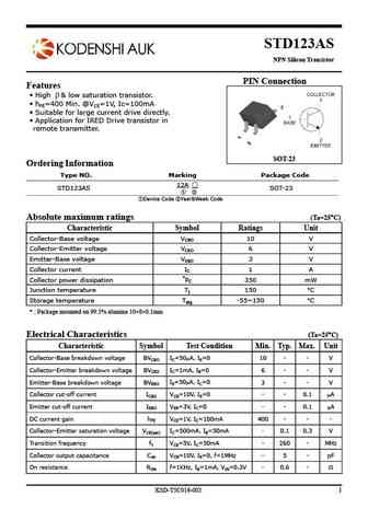
STD123AS NPN Silicon Transistor PIN Connection Features High & low saturation transistor. hFE=400 Min. @VCE=1V, Ic=100mA Suitable for large current drive directly. Application for IRED Drive transistor in remote transmitter. SOT-23 Ordering Information Type NO. Marking Package Code 12A STD123AS SOT-23 Device Code Year&Week Co... See More ⇒
9.27. Size:257K auk
std123asf.pdf 

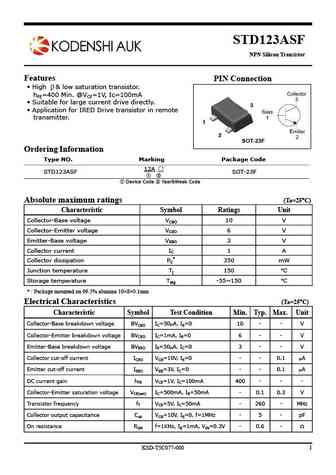
STD123ASF NPN Silicon Transistor Features PIN Connection High & low saturation transistor. hFE=400 Min. @VCE=1V, Ic=100mA Suitable for large current drive directly. 3 Application for IRED Drive transistor in remote transmitter. 1 2 SOT-23F Ordering Information Type NO. Marking Package Code 12A STD123ASF SOT-23F Device Code ... See More ⇒
9.28. Size:245K auk
std123u.pdf 

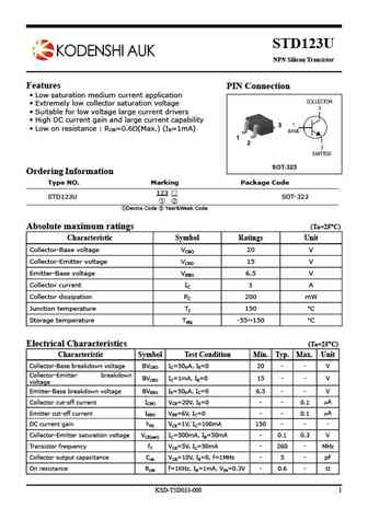
STD123U NPN Silicon Transistor Features PIN Connection Low saturation medium current application Extremely low collector saturation voltage Suitable for low voltage large current drivers High DC current gain and large current capability 3 Low on resistance RON=0.6 (Max.) (IB=1mA) 1 2 SOT-323 Ordering Information Type NO. Marking Package Cod... See More ⇒
9.29. Size:174K auk
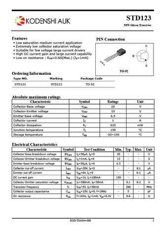
std123.pdf 

STD123 NPN Silicon Transistor Features PIN Connection Low saturation medium current application C Extremely low collector saturation voltage Suitable for low voltage large current drivers High DC current gain and large current capability B Low on resistance RON=0.6 (Max.) (IB=1mA) E TO-92 Ordering Information Type NO. Marking Package Code ... See More ⇒
9.30. Size:202K auk
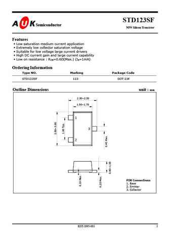
std123sf.pdf 

STD123SF Semiconductor Semiconductor NPN Silicon Transistor Features Low saturation medium current application Extremely low collector saturation voltage Suitable for low voltage large current drivers High DC current gain and large current capability Low on resistance RON=0.6 (Max.) (IB=1mA) Ordering Information Type NO. Marking Package Code S... See More ⇒
9.31. Size:707K jiangsu
std123s.pdf 

JIANGSU CHANGJING ELECTRONICS TECHNOLOGY CO., LTD SOT-23 Plastic-Encapsulate Transistors STD123S TRANSISTOR (NPN) SOT-23 FEATURES Low saturation medium current application 1. BASE Extremely low collector saturation voltage 2. EMITTER Suitable for low voltage large current drivers 3. COLLECTOR High DC current gain and large current capability Low on resistance RON=0.6 (M... See More ⇒
9.32. Size:939K htsemi
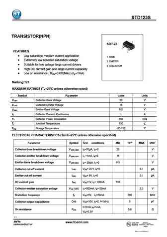
std123s.pdf 

STD1 23S TRANSISTOR(NPN) SOT-23 FEATURES Low saturation medium current application 1. BASE Extremely low collector saturation voltage 2. EMITTER Suitable for low voltage large current drivers 3. COLLECTOR High DC current gain and large current capability Low on resistance RON=0.6 (Max.) (IB=1mA) Marking 123 MAXIMUM RATINGS (TA=25 unless otherwise noted)... See More ⇒
9.33. Size:211K lge
std123s.pdf 

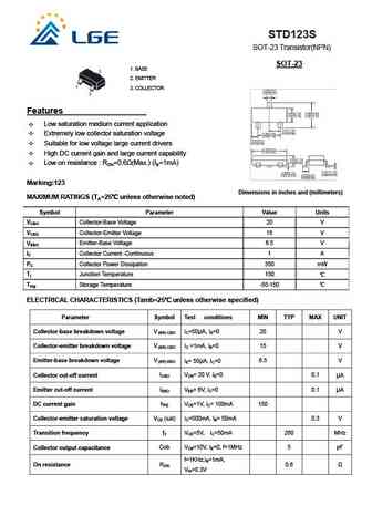
STD123S SOT-23 Transistor(NPN) SOT-23 1. BASE 2. EMITTER 3. COLLECTOR Features Low saturation medium current application Extremely low collector saturation voltage Suitable for low voltage large current drivers High DC current gain and large current capability Low on resistance RON=0.6 (Max.) (IB=1mA) Marking 123 Dimensions in inches and (millimeters) MA... See More ⇒
9.34. Size:90K samhop
std12l01a.pdf 

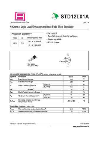
Gr P Pr P P STD12L01A a S mHop Microelectronics C orp. Ver 2.0 N-Channel Logic Level Enhancement Mode Field Effect Transistor FEATURES PRODUCT SUMMARY Super high dense cell design for low RDS(ON). RDS(ON) (m ) Max VDSS ID Rugged and reliable. 140 @ VGS=10V TO-251 Package. 12A 100V 170 @ VGS=4.5V STD SERIES ( ) TO - 251 I - PAK (TA=25 C unless otherwise noted) ABSOLUTE... See More ⇒
9.35. Size:91K samhop
std12l01.pdf 

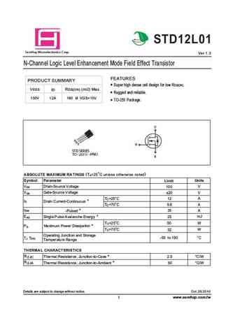
Gre r r P Pr Pr Pro STD12L01 a S mHop Microelectronics C orp. Ver 1.3 N-Channel Logic Level Enhancement Mode Field Effect Transistor FEATURES PRODUCT SUMMARY Super high dense cell design for low RDS(ON). RDS(ON) (m ) Max VDSS ID Rugged and reliable. 100V 12A 160 @ VGS=10V TO-251 Package. STD SERIES ( ) TO - 251 I - PAK (TA=25 C unless otherwise noted) ABSOLUTE MAXIMUM R... See More ⇒
Detailed specifications: STC5551F, STC945, STD123, STD123AS, STD123ASF, STD123SF, STD123U, STD123UF, NJW0281G, STD1664, STD1766, STD1862, STD1862L, STD361, STD6528EF, STD6528S, STN2222
Keywords - STD129 pdf specs
STD129 cross reference
STD129 equivalent finder
STD129 pdf lookup
STD129 substitution
STD129 replacement
![]()
![]()
