2N6306T3 Specs and Replacement
Type Designator: 2N6306T3
Material of Transistor: Si
Polarity: NPN
Absolute Maximum Ratings
Maximum Collector Power Dissipation (Pc): 125 W
Maximum Collector-Base Voltage |Vcb|: 500 V
Maximum Collector-Emitter Voltage |Vce|: 250 V
Maximum Emitter-Base Voltage |Veb|: 8 V
Maximum Collector Current |Ic max|: 8 A
Max. Operating Junction Temperature (Tj): 200 °C
Electrical Characteristics
Transition Frequency (ft): 5 MHz
Collector Capacitance (Cc): 250 pF
Forward Current Transfer Ratio (hFE), MIN: 15
Package: TO254AA
2N6306T3 Substitution
- BJT ⓘ Cross-Reference Search
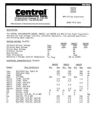
2N6306T3 datasheet
145 Adams Avenue, Hauppauge, NY 11788 USA Tel (631) 435-1110 Fax (631) 435-1824 ... See More ⇒
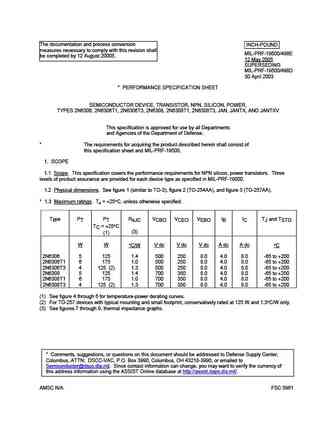
The documentation and process conversion INCH-POUND measures necessary to comply with this revision shall MIL-PRF-19500/498E be completed by 12 August 20005. 12 May 2005 SUPERSEDING MIL-PRF-19500/498D 30 April 2003 * PERFORMANCE SPECIFICATION SHEET SEMICONDUCTOR DEVICE, TRANSISTOR, NPN, SILICON, POWER, TYPES 2N6306, 2N6306T1, 2N6306T3, 2N6308, 2N6308T1, 2N6308T3, JAN, J... See More ⇒
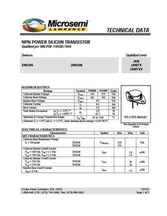
TECHNICAL DATA NPN POWER SILICON TRANSISTOR Qualified per MIL-PRF-19500/498 Devices Qualified Level JAN 2N6306 2N6308 JANTX JANTXV MAXIMUM RATINGS Ratings Symbol 2N6306 2N6308 Units Collector-Emitter Voltage 250 350 Vdc VCEO Collector-Base Voltage 500 700 Vdc VCBO Emitter-Base Voltage 8.0 Vdc VEBO Collector Current 8.0 Adc IC Base Current 4.0 Adc IB Total P... See More ⇒
Inchange Semiconductor Product Specification Silicon NPN Power Transistors 2N6306 DESCRIPTION With TO-3 package High breakdown voltage High power dissipation APPLICATIONS Designed for high voltage inverters, switching regulators,line operated amplifiers, and switching power supplies applications PINNING (See Fig.2) PIN DESCRIPTION 1 Base 2 Emitter Fig.1 simplif... See More ⇒
Detailed specifications: 2N6922A, 2N6923, 2N6923A, 2N6926, 2N6926A, 2N6927, 2N6927A, 2N6306T1, BC558, 2N6308T1, 2N6308T3, 2N916CSM, 2N916DCSM, 2N918ADCSM, 2N918DCSM, 2N930UB, 2N6338X
Keywords - 2N6306T3 pdf specs
2N6306T3 cross reference
2N6306T3 equivalent finder
2N6306T3 pdf lookup
2N6306T3 substitution
2N6306T3 replacement


