2N3998SMD05 Specs and Replacement
Type Designator: 2N3998SMD05
Material of Transistor: Si
Polarity: NPN
Absolute Maximum Ratings
Maximum Collector Power Dissipation (Pc): 20 W
Maximum Collector-Emitter Voltage |Vce|: 80 V
Maximum Collector Current |Ic max|: 5 A
Electrical Characteristics
Transition Frequency (ft): 40 MHz
Forward Current Transfer Ratio (hFE), MIN: 40
Noise Figure, dB: -
Package: TO276AA
- BJT ⓘ Cross-Reference Search
2N3998SMD05 datasheet
..1. Size:11K semelab
2n3998smd05.pdf 

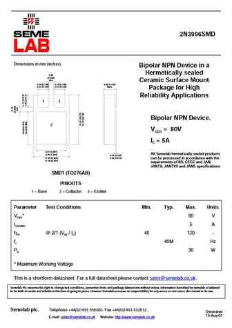
2N3998SMD05 Dimensions in mm (inches). Bipolar NPN Device in a Hermetically sealed 7.54 (0.296) 0.76 (0.030) Ceramic Surface Mount min. 3.175 (0.125) 2.41 (0.095) Package for High 2.41 (0.095) Max. 0.127 (0.005) Reliability Applications 1 3 Bipolar NPN Device. 2 VCEO = 80V IC = 5A 0.127 (0.005) 16 PLCS 0.127 (0.005) 0.50(0.020) 0.50 (0.020) All Semelab herm... See More ⇒
5.1. Size:10K semelab
2n3998smd.pdf

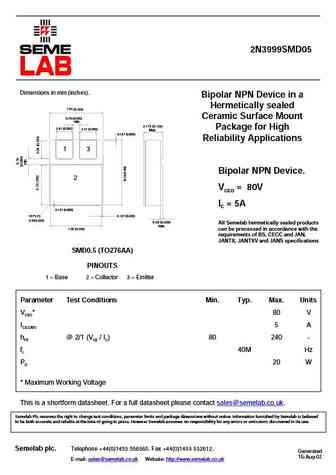
2N3998SMD Dimensions in mm (inches). Bipolar NPN Device in a Hermetically sealed 0.89 (0.035) min. Ceramic Surface Mount 3.70 (0.146) 3.70 (0.146) 3.60 (0.142) 3.41 (0.134) 3.41 (0.134) Max. Package for High Reliability Applications 1 3 Bipolar NPN Device. 2 VCEO = 80V IC = 5A 9.67 (0.381) All Semelab hermetically sealed products 9.38 (0.369) 0.50 (0.020) 0.26 (0... See More ⇒
9.1. Size:10K semelab
2n3996smd05.pdf

2N3996SMD05 Dimensions in mm (inches). Bipolar NPN Device in a Hermetically sealed 7.54 (0.296) 0.76 (0.030) Ceramic Surface Mount min. 3.175 (0.125) 2.41 (0.095) Package for High 2.41 (0.095) Max. 0.127 (0.005) Reliability Applications 1 3 Bipolar NPN Device. 2 VCEO = 80V IC = 5A 0.127 (0.005) 16 PLCS 0.127 (0.005) 0.50(0.020) 0.50 (0.020) All Semelab herm... See More ⇒
9.2. Size:10K semelab
2n3996smd.pdf
2N3996SMD Dimensions in mm (inches). Bipolar NPN Device in a Hermetically sealed 0.89 (0.035) min. Ceramic Surface Mount 3.70 (0.146) 3.70 (0.146) 3.60 (0.142) 3.41 (0.134) 3.41 (0.134) Max. Package for High Reliability Applications 1 3 Bipolar NPN Device. 2 VCEO = 80V IC = 5A 9.67 (0.381) All Semelab hermetically sealed products 9.38 (0.369) 0.50 (0.020) 0.26 (0... See More ⇒
9.3. Size:10K semelab
2n3999smd05.pdf
2N3999SMD05 Dimensions in mm (inches). Bipolar NPN Device in a Hermetically sealed 7.54 (0.296) 0.76 (0.030) Ceramic Surface Mount min. 3.175 (0.125) 2.41 (0.095) Package for High 2.41 (0.095) Max. 0.127 (0.005) Reliability Applications 1 3 Bipolar NPN Device. 2 VCEO = 80V IC = 5A 0.127 (0.005) 16 PLCS 0.127 (0.005) 0.50(0.020) 0.50 (0.020) All Semelab herm... See More ⇒
9.4. Size:10K semelab
2n3999smd.pdf

2N3999SMD Dimensions in mm (inches). Bipolar NPN Device in a Hermetically sealed 0.89 (0.035) min. Ceramic Surface Mount 3.70 (0.146) 3.70 (0.146) 3.60 (0.142) 3.41 (0.134) 3.41 (0.134) Max. Package for High Reliability Applications 1 3 Bipolar NPN Device. 2 VCEO = 80V IC = 5A 9.67 (0.381) All Semelab hermetically sealed products 9.38 (0.369) 0.50 (0.020) 0.26 (0... See More ⇒
9.5. Size:10K semelab
2n3997smd.pdf

2N3997SMD Dimensions in mm (inches). Bipolar NPN Device in a Hermetically sealed 0.89 (0.035) min. Ceramic Surface Mount 3.70 (0.146) 3.70 (0.146) 3.60 (0.142) 3.41 (0.134) 3.41 (0.134) Max. Package for High Reliability Applications 1 3 Bipolar NPN Device. 2 VCEO = 80V IC = 5A 9.67 (0.381) All Semelab hermetically sealed products 9.38 (0.369) 0.50 (0.020) 0.26 (0... See More ⇒
9.6. Size:10K semelab
2n3997smd05.pdf

2N3997SMD05 Dimensions in mm (inches). Bipolar NPN Device in a Hermetically sealed 7.54 (0.296) 0.76 (0.030) Ceramic Surface Mount min. 3.175 (0.125) 2.41 (0.095) Package for High 2.41 (0.095) Max. 0.127 (0.005) Reliability Applications 1 3 Bipolar NPN Device. 2 VCEO = 80V IC = 5A 0.127 (0.005) 16 PLCS 0.127 (0.005) 0.50(0.020) 0.50 (0.020) All Semelab herm... See More ⇒
9.7. Size:93K interfet
2n3993-a.pdf
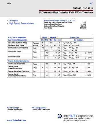
Databook.fxp 1/13/99 2 09 PM Page B-7 01/99 B-7 2N3993, 2N3993A P-Channel Silicon Junction Field-Effect Transistor Absolute maximum ratings at TA = 25 C Choppers Reverse Gate Source & Reverse Gate Drain Voltage 25 V High Speed Commutators Continuous Forward Gate Current 10 mA Continuous Device Power Dissipation 300 mW Power Derating 2.4 mW/ C At 25 C free air temperature... See More ⇒
9.8. Size:92K interfet
2n3994-a.pdf
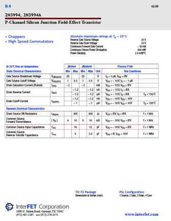
Databook.fxp 1/13/99 2 09 PM Page B-8 B-8 01/99 2N3994, 2N3994A P-Channel Silicon Junction Field-Effect Transistor Absolute maximum ratings at TA = 25 C Choppers Reverse Gate Source Voltage 25 V High Speed Commutators Reverse Gate Drain Voltage 25 V Continuous Forward Gate Current 10 mA Continuous Device Power Dissipation 300 mW Power Derating 2.4 mW/ C At 25 C free air... See More ⇒
9.9. Size:54K microsemi
2n3996-99.pdf
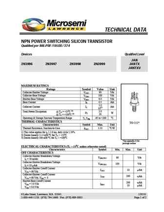
TECHNICAL DATA NPN POWER SWITCHING SILICON TRANSISTOR Qualified per MIL-PRF-19500/374 Devices Qualified Level JAN 2N3996 2N3997 2N3998 2N3999 JANTX JANTXV MAXIMUM RATINGS Ratings Symbol Value Unit Collector-Emitter Voltage 80 Vdc VCEO Collector-Base Voltage 100 Vdc VCBO Emitter-Base Voltage 8.0 Vdc VEBO Base Current I 0.5 Adc B 5.0 Collector Current IC Adc ... See More ⇒
Detailed specifications: 2N3906N, 2N3906SC, 2N3964DCSM, 2N3996SMD, 2N3996SMD05, 2N3997SMD, 2N3997SMD05, 2N3998SMD, 13003, 2N3999SMD, 2N3999SMD05, 2N4033UB, 2N4124G, 2N4150S, 2N4209C1A, 2N4209C1B, 2N4236X
Keywords - 2N3998SMD05 pdf specs
2N3998SMD05 cross reference
2N3998SMD05 equivalent finder
2N3998SMD05 pdf lookup
2N3998SMD05 substitution
2N3998SMD05 replacement
