MJD112G Datasheet. Specs and Replacement
Type Designator: MJD112G 📄📄
SMD Transistor Code: J112G
Material of Transistor: Si
Polarity: NPN
Absolute Maximum Ratings
Maximum Collector Power Dissipation (Pc): 20 W
Maximum Collector-Base Voltage |Vcb|: 100 V
Maximum Collector-Emitter Voltage |Vce|: 100 V
Maximum Emitter-Base Voltage |Veb|: 5 V
Maximum Collector Current |Ic max|: 2 A
Max. Operating Junction Temperature (Tj): 150 °C
Electrical Characteristics
Transition Frequency (ft): 25 MHz
Collector Capacitance (Cc): 100 pF
Forward Current Transfer Ratio (hFE), MIN: 1000
Noise Figure, dB: -
Package: TO-252
- BJT ⓘ Cross-Reference Search
MJD112G datasheet
..1. Size:224K onsemi
mjd112g.pdf 

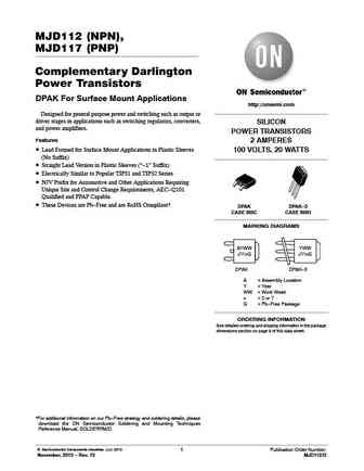
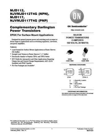
MJD112, NJVMJD112T4G (NPN), MJD117, NJVMJD117T4G (PNP) Complementary Darlington http //onsemi.com Power Transistors SILICON DPAK For Surface Mount Applications POWER TRANSISTORS Designed for general purpose power and switching such as output or 2 AMPERES driver stages in applications such as switching regulators, converters, 100 VOLTS, 20 WATTS and power amplifiers. Features ... See More ⇒
8.1. Size:306K motorola
mjd112 mjd117.pdf 

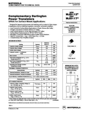
Order this document MOTOROLA by MJD112/D SEMICONDUCTOR TECHNICAL DATA NPN * MJD112 Complementary Darlington PNP MJD117* Power Transistors DPAK For Surface Mount Applications *Motorola Preferred Device Designed for general purpose power and switching such as output or driver stages SILICON in applications such as switching regulators, converters, and power amplifiers. POWER TRANS... See More ⇒
8.3. Size:152K fairchild semi
mjd112.pdf 

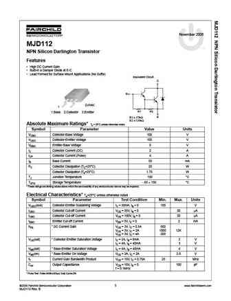
November 2006 MJD112 tm NPN Silicon Darlington Transistor Features High DC Current Gain Built-in a Damper Diode at E-C Lead Formed for Surface Mount Applications (No Suffix) Equivalent Circuit C B D-PAK 1 R1 R2 1.Base 2.Collector 3.Emitter E R1 10k R2 0.6k Absolute Maximum Ratings* Ta = 25 C unless otherwise noted Symbol Parameter Value Units VC... See More ⇒
8.4. Size:153K onsemi
njvmjd112 njvmjd117.pdf 

MJD112 (NPN), MJD117 (PNP) Complementary Darlington Power Transistors DPAK For Surface Mount Applications http //onsemi.com Designed for general purpose power and switching such as output or driver stages in applications such as switching regulators, converters, SILICON and power amplifiers. POWER TRANSISTORS Features 2 AMPERES Lead Formed for Surface Mount Applications in Plas... See More ⇒
8.5. Size:224K onsemi
mjd112rlg.pdf 

MJD112, NJVMJD112T4G (NPN), MJD117, NJVMJD117T4G (PNP) Complementary Darlington http //onsemi.com Power Transistors SILICON DPAK For Surface Mount Applications POWER TRANSISTORS Designed for general purpose power and switching such as output or 2 AMPERES driver stages in applications such as switching regulators, converters, 100 VOLTS, 20 WATTS and power amplifiers. Features ... See More ⇒
8.6. Size:224K onsemi
mjd112t4g.pdf 

MJD112, NJVMJD112T4G (NPN), MJD117, NJVMJD117T4G (PNP) Complementary Darlington http //onsemi.com Power Transistors SILICON DPAK For Surface Mount Applications POWER TRANSISTORS Designed for general purpose power and switching such as output or 2 AMPERES driver stages in applications such as switching regulators, converters, 100 VOLTS, 20 WATTS and power amplifiers. Features ... See More ⇒
8.7. Size:224K onsemi
mjd112-1g.pdf 

MJD112, NJVMJD112T4G (NPN), MJD117, NJVMJD117T4G (PNP) Complementary Darlington http //onsemi.com Power Transistors SILICON DPAK For Surface Mount Applications POWER TRANSISTORS Designed for general purpose power and switching such as output or 2 AMPERES driver stages in applications such as switching regulators, converters, 100 VOLTS, 20 WATTS and power amplifiers. Features ... See More ⇒
8.8. Size:84K cdil
mjd112 mjd117.pdf 

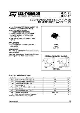
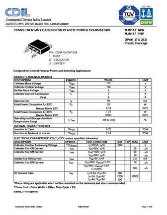
Continental Device India Limited An ISO/TS 16949, ISO 9001 and ISO 14001 Certified Company COMPLEMENTARY DARLINGTON PLASTIC POWER TRANSISTORS MJD112 NPN MJD117 PNP DPAK (TO-252) Plastic Package Designed for General Purpose Power and Switching Applications ABSOLUTE MAXIMUM RATINGS DESCRIPTION SYMBOL VALUE UNIT VCBO 100 Collector Base Voltage V VCEO 100 Collector Emitter Voltage V E... See More ⇒
8.9. Size:394K kec
mjd112 l.pdf 

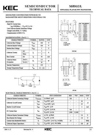
SEMICONDUCTOR MJD112/L TECHNICAL DATA EPITAXIAL PLANAR NPN TRANSISTOR MONOLITHIC CONSTRUCTION WITH BUILT IN BASE-EMITTER SHUNT RESISTORS INDUSTRIAL USE. A I C J FEATURES DIM MILLIMETERS High DC Current Gain. _ A 6.60 + 0.2 _ B 6.10 + 0.2 hFE=1000(Min.), VCE=4V, IC=1A. _ C 5.0 + 0.2 _ D 1.10 + 0.2 Low Collector-Emitter Saturation Voltage. _ E 2.70 + 0.2 _ F 2.30 + 0... See More ⇒
8.10. Size:184K lge
mjd112.pdf 

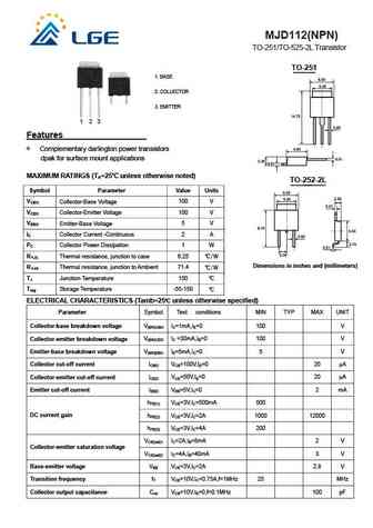
MJD112(NPN) TO-251/TO-525-2L Transistor TO-251 1. BASE 2. COLLECTOR 3. EMITTER 1 2 3 Features Complementary darlington power transistors dpak for surface mount applications MAXIMUM RATINGS (TA=25 unless otherwise noted) TO-252-2L Symbol Parameter Value Units VCBO 100 V Collector-Base Voltage VCEO 100 V Collector-Emitter Voltage VEBO 5 V Emitter-Base Voltage ... See More ⇒
Detailed specifications: MJB44H11G, MJB44H11T4, MJB44H11T4-A, MJB44H11T4G, MJB45H11G, MJB45H11T4G, MJB5742T4G, MJD112-1G, 13003, MJD112RLG, MJD112T4G, MJD117-1G, MJD117G, MJD117T4G, MJD122G, MJD122T4G, MJD127G
Keywords - MJD112G pdf specs
MJD112G cross reference
MJD112G equivalent finder
MJD112G pdf lookup
MJD112G substitution
MJD112G replacement

