2N5550TFR Specs and Replacement
Type Designator: 2N5550TFR
Material of Transistor: Si
Polarity: NPN
Absolute Maximum Ratings
Maximum Collector Power Dissipation (Pc): 0.625 W
Maximum Collector-Base Voltage |Vcb|: 160 V
Maximum Collector-Emitter Voltage |Vce|: 140 V
Maximum Emitter-Base Voltage |Veb|: 6 V
Maximum Collector Current |Ic max|: 0.6 A
Max. Operating Junction Temperature (Tj): 150 °C
Electrical Characteristics
Transition Frequency (ft): 100 MHz
Collector Capacitance (Cc): 6 pF
Forward Current Transfer Ratio (hFE), MIN: 60
Noise Figure, dB: -
Package: TO92
- BJT ⓘ Cross-Reference Search
2N5550TFR datasheet
8.1. Size:188K motorola
2n5550 2n5551.pdf 

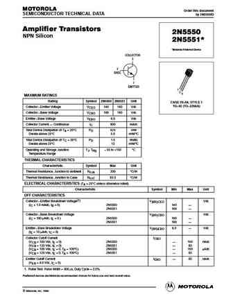
MOTOROLA Order this document SEMICONDUCTOR TECHNICAL DATA by 2N5550/D Amplifier Transistors 2N5550 NPN Silicon * 2N5551 *Motorola Preferred Device COLLECTOR 3 2 BASE 1 EMITTER 1 2 3 MAXIMUM RATINGS Rating Symbol 2N5550 2N5551 Unit CASE 29 04, STYLE 1 TO 92 (TO 226AA) Collector Emitter Voltage VCEO 140 160 Vdc Collector Base Voltage VCBO 160 180 Vdc Emitter B... See More ⇒
8.2. Size:53K philips
2n5550 2n5551 2.pdf 

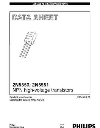
DISCRETE SEMICONDUCTORS DATA SHEET book, halfpage M3D186 2N5550; 2N5551 NPN high-voltage transistors Product specification 2004 Oct 28 Supersedes data of 1999 Apr 23 Philips Semiconductors Product specification NPN high-voltage transistors 2N5550; 2N5551 FEATURES PINNING Low current (max. 300 mA) PIN DESCRIPTION High voltage (max. 160 V). 1 collector 2 base APPLICATIONS... See More ⇒
8.3. Size:329K fairchild semi
2n5550.pdf 

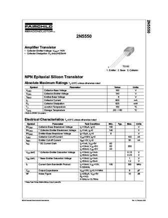
AmpIifier Transistor Collector-Emitter Voltage VCEO= 140V Collector Dissipation PC (max)=625mW TO-92 1. Emitter 2. Base 3. Collector NPN EpitaxiaI SiIicon Transistor AbsoIute Maximum Ratings Ta=25 C unless otherwise noted SymboI Parameter VaIue Units VCBO Collector-Base Voltage 160 V VCEO Collector-Emitter Voltage 140 V VEBO Emitter-Base Voltage 6 V IC ... See More ⇒
8.5. Size:88K onsemi
2n5550 2n5551.pdf 

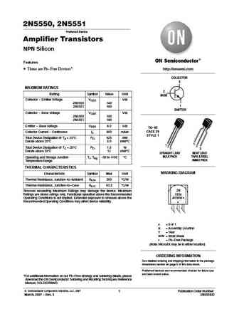
2N5550, 2N5551 Preferred Device Amplifier Transistors NPN Silicon Features These are Pb-Free Devices* http //onsemi.com COLLECTOR 3 MAXIMUM RATINGS 2 Rating Symbol Value Unit BASE Collector - Emitter Voltage VCEO Vdc 2N5550 140 1 2N5551 160 EMITTER Collector - Base Voltage VCBO Vdc 2N5550 160 2N5551 180 Emitter - Base Voltage VEBO 6.0 Vdc TO-92 CASE 29 Collector Curr... See More ⇒
8.6. Size:88K onsemi
2n5550g.pdf 

2N5550, 2N5551 Preferred Device Amplifier Transistors NPN Silicon Features These are Pb-Free Devices* http //onsemi.com COLLECTOR 3 MAXIMUM RATINGS 2 Rating Symbol Value Unit BASE Collector - Emitter Voltage VCEO Vdc 2N5550 140 1 2N5551 160 EMITTER Collector - Base Voltage VCBO Vdc 2N5550 160 2N5551 180 Emitter - Base Voltage VEBO 6.0 Vdc TO-92 CASE 29 Collector Curr... See More ⇒
8.7. Size:334K onsemi
2n5550.pdf 

Is Now Part of To learn more about ON Semiconductor, please visit our website at www.onsemi.com Please note As part of the Fairchild Semiconductor integration, some of the Fairchild orderable part numbers will need to change in order to meet ON Semiconductor s system requirements. Since the ON Semiconductor product management systems do not have the ability to manage part nomenclatur... See More ⇒
8.8. Size:122K secos
2n5550.pdf 

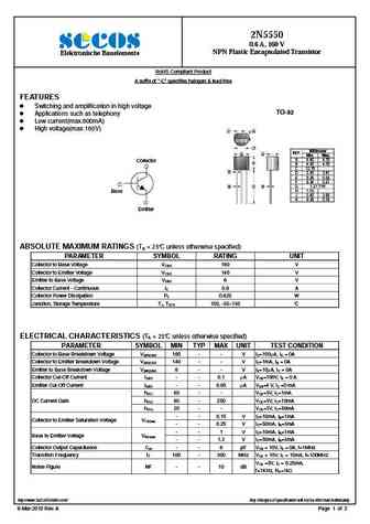
2N5550 0.6 A, 160 V NPN Plastic Encapsulated Transistor Elektronische Bauelemente RoHS Compliant Product A suffix of -C specifies halogen & lead-free FEATURES Switching and amplification in high voltage TO-92 Applications such as telephony Low current(max.600mA) High voltage(max.160V) G H J Millimeter REF. A D Min. Max. A 4.40 4.70 Collector B ... See More ⇒
8.9. Size:206K cdil
2n5550.pdf 

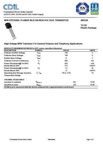
Continental Device India Limited An ISO/TS 16949, ISO 9001 and ISO 14001 Certified Company NPN EPITAXIAL PLANAR SILICON HIGH VOLTAGE TRANSISTOR 2N5550 TO-92 Plastic Package High Voltage NPN Transistor For General Purpose and Telephony Applications. ABSOLUTE MAXIMUM RATINGS(Ta=25 C unless specified otherwise) DESCRIPTION SYMBOL VALUE UNITS VCEO Collector Emitter Voltage 140 V VCBO ... See More ⇒
8.10. Size:624K jiangsu
2n5550.pdf 

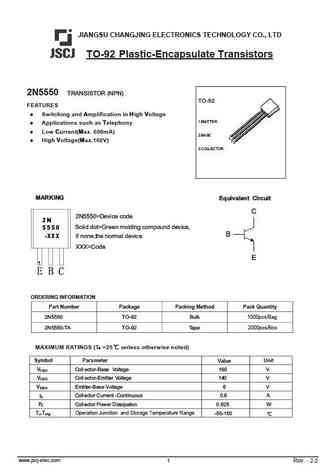
JIANGSU CHANGJING ELECTRONICS TECHNOLOGY CO., LTD TO-92 Plastic-Encapsulate Transistors 2N5550 TRANSISTOR (NPN) TO-92 FEATURES Switching and mplification in igh oltage 1.EMITTER Applications such as elephony Low urrent( ax. 600mA) 2.BASE High oltage( ax.160V) 3.COLLECTOR Equivalent Circuit 2N5550=Device code 2N Solid dot=Green molding compound device... See More ⇒
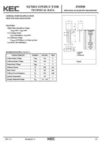
8.11. Size:32K kec
2n5550.pdf 

SEMICONDUCTOR 2N5550 TECHNICAL DATA EPITAXIAL PLANAR NPN TRANSISTOR GENERAL PURPOSE APPLICATION. HIGH VOLTAGE APPLICATION. B C FEATURES High Collector Breakdwon Voltage N DIM MILLIMETERS VCBO=160V, VCEO=140V A 4.70 MAX E K Low Leakage Current. B 4.80 MAX G C 3.70 MAX D ICBO=100nA(Max.), VCB=100V D 0.45 E 1.00 Low Saturation Voltage F 1.27 G 0.85 VCE(sat)=0.25V(Max.)... See More ⇒
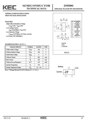
8.12. Size:33K kec
2n5550s.pdf 

SEMICONDUCTOR 2N5550S TECHNICAL DATA EPITAXIAL PLANAR NPN TRANSISTOR GENERAL PURPOSE APPLICATION. HIGH VOLTAGE APPLICATION. E L B L DIM MILLIMETERS FEATURES _ + 2.93 0.20 A B 1.30+0.20/-0.15 High Collector Breakdwon Voltage C 1.30 MAX 2 VCBO=160V, VCEO=140V 3 D 0.45+0.15/-0.05 E 2.40+0.30/-0.20 Low Leakage Current. 1 G 1.90 H 0.95 ICBO=100nA(Max.) VCB=100V J 0.13+0.... See More ⇒
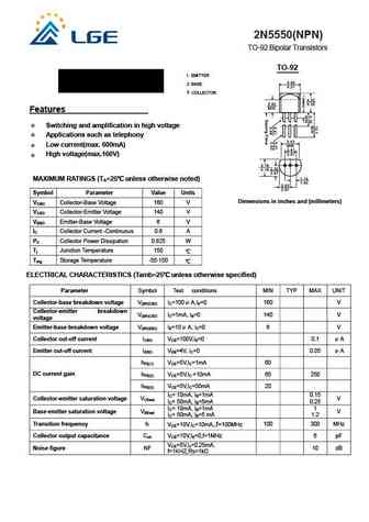
8.13. Size:199K lge
2n5550.pdf 

2N5550(NPN) TO-92 Bipolar Transistors TO-92 1. EMITTER 2. BASE 3. COLLECTOR Features Switching and amplification in high voltage Applications such as telephony Low current(max. 600mA) High voltage(max.160V) MAXIMUM RATINGS (TA=25 unless otherwise noted) Symbol Parameter Value Units Dimensions in inches and (millimeters) VCBO Collector-Base Voltage 160 V V... See More ⇒
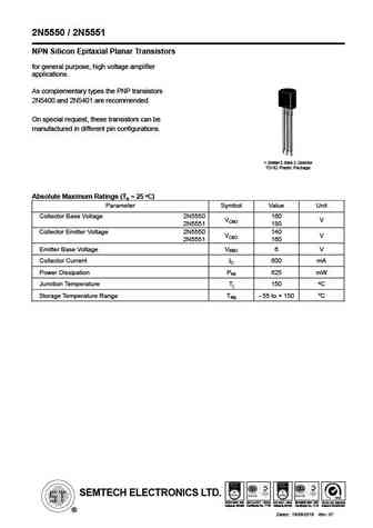
8.14. Size:152K semtech
2n5550 2n5551.pdf 

2N5550 / 2N5551 NPN Silicon Epitaxial Planar Transistors for general purpose, high voltage amplifier applications. As complementary types the PNP transistors 2N5400 and 2N5401 are recommended. On special request, these transistors can be manufactured in different pin configurations. 1. Emitter 2. Base 3. Collector TO-92 Plastic Package O Absolute Maximum Ratings (Ta = 25 C)... See More ⇒
8.15. Size:1188K first silicon
2n5550-1s.pdf 
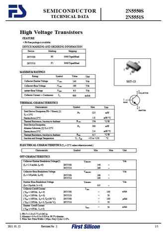
SEMICONDUCTOR 2N5550S TECHNICAL DATA 2N5551S High Voltage Transistors FEATURE Pb-Free package is available. DEVICE MARKING AND ORDERING INFORMATION Device Marking Shipping F0 3000/Tape&Reel 2N5550S 3 F1 3000/Tape&Reel 2N5551S 1 MAXIMUM RATINGS 2 Rating Symbol Value Unit Collector Emitter Voltage V CEO 140 Vdc SOT 23 Collector Base Voltage V CBO 160 Vdc ... See More ⇒
Detailed specifications: 2N4403TF
, 2N4403TFR
, 2N5401YBU
, 2N5401YTA
, 2N5550BU
, 2N5550TA
, 2N5550TAR
, 2N5550TF
, BC547
, 2N5551BU
, 2N5551TA
, 2N5551TF
, 2N5551TFR
, 2N6517BU
, 2N6517CTA
, 2N6517TA
, 2SA1943OTU
.
Keywords - 2N5550TFR pdf specs
2N5550TFR cross reference
2N5550TFR equivalent finder
2N5550TFR pdf lookup
2N5550TFR substitution
2N5550TFR replacement
