2SA650 Datasheet. Specs and Replacement
Type Designator: 2SA650
Material of Transistor: Si
Polarity: PNP
Absolute Maximum Ratings
Maximum Collector Power Dissipation (Pc): 100 W
Maximum Collector-Base Voltage |Vcb|: 150 V
Maximum Collector-Emitter Voltage |Vce|: 100 V
Maximum Emitter-Base Voltage |Veb|: 5 V
Maximum Collector Current |Ic max|: 10 A
Max. Operating Junction Temperature (Tj): 150 °C
Electrical Characteristics
Transition Frequency (ft): 5 MHz
Collector Capacitance (Cc): 500 pF
Forward Current Transfer Ratio (hFE), MIN: 70
Noise Figure, dB: -
Package: TO3
- BJT ⓘ Cross-Reference Search
2SA650 datasheet
..1. Size:189K inchange semiconductor
2sa650.pdf 
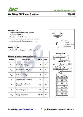
isc Silicon PNP Power Transistor 2SA650 DESCRIPTION Collector-Emitter Breakdown Voltage- V = -150V(Min.) (BR)CEO Wide Area of Safe Operation Minimum Lot-to-Lot variations for robust device performance and reliable operation APPLICATIONS Designed for audio power amplifier applications. ABSOLUTE MAXIMUM RATINGS(T =25 ) a SYMBOL PARAMETER VALUE UNIT V Collector-Base Voltag... See More ⇒
9.1. Size:145K jmnic
2sa658.pdf
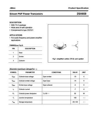
JMnic Product Specification Silicon PNP Power Transistors 2SA658 DESCRIPTION With TO-3 package Wide area of safe operation Complement to type 2SC521 APPLICATIONS For audio frequency and power amplifier applications PINNING(see Fig.2) PIN DESCRIPTION 1 Base 2 Emitter Fig.1 simplified outline (TO-3) and symbol 3 Collector Absolute maximum ratings(Ta= ) SYMBOL... See More ⇒
9.2. Size:145K jmnic
2sa656.pdf

JMnic Product Specification Silicon PNP Power Transistors 2SA656 DESCRIPTION With TO-3 package Wide area of safe operation Complement to type 2SC519 APPLICATIONS For audio frequency and power amplifier applications PINNING(see Fig.2) PIN DESCRIPTION 1 Base 2 Emitter Fig.1 simplified outline (TO-3) and symbol 3 Collector Absolute maximum ratings(Ta= ) SYMBOL... See More ⇒
9.3. Size:145K jmnic
2sa657.pdf
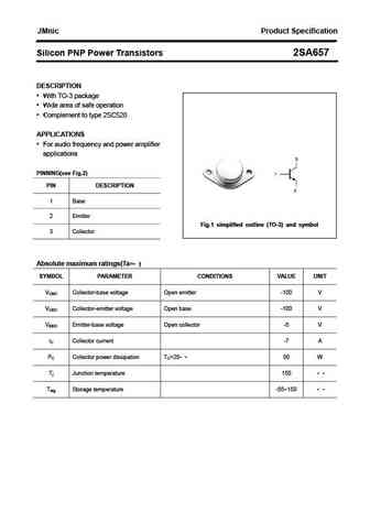
JMnic Product Specification Silicon PNP Power Transistors 2SA657 DESCRIPTION With TO-3 package Wide area of safe operation Complement to type 2SC520 APPLICATIONS For audio frequency and power amplifier applications PINNING(see Fig.2) PIN DESCRIPTION 1 Base 2 Emitter Fig.1 simplified outline (TO-3) and symbol 3 Collector Absolute maximum ratings(Ta= ) SYMBOL... See More ⇒
9.4. Size:189K inchange semiconductor
2sa658.pdf
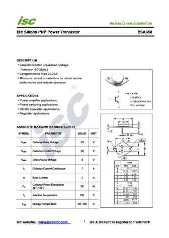
isc Silicon PNP Power Transistor 2SA658 DESCRIPTION Collector-Emitter Breakdown Voltage- V = -50V(Min.) (BR)CEO Complement to Type 2SC521 Minimum Lot-to-Lot variations for robust device performance and reliable operation APPLICATIONS Power amplifier applications. Power switching applications. DC-DC converter applications. Regulator applications. ABSOLUTE MAXIMUM RAT... See More ⇒
9.5. Size:189K inchange semiconductor
2sa651.pdf
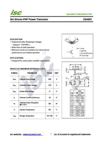
isc Silicon PNP Power Transistor 2SA651 DESCRIPTION Collector-Emitter Breakdown Voltage- V = -150V(Min.) (BR)CEO Wide Area of Safe Operation Minimum Lot-to-Lot variations for robust device performance and reliable operation APPLICATIONS Designed for audio power amplifier applications. ABSOLUTE MAXIMUM RATINGS(T =25 ) a SYMBOL PARAMETER VALUE UNIT V Collector-Base Voltag... See More ⇒
9.6. Size:187K inchange semiconductor
2sa656.pdf
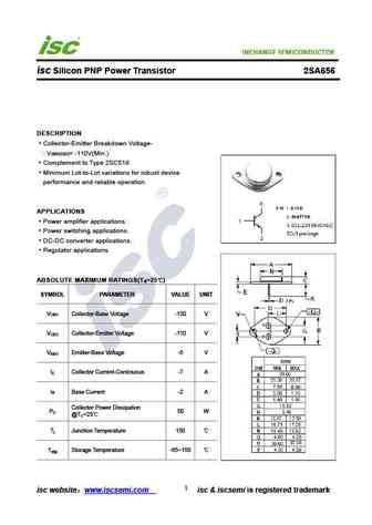
isc Silicon PNP Power Transistor 2SA656 DESCRIPTION Collector-Emitter Breakdown Voltage- V = -110V(Min.) (BR)CEO Complement to Type 2SC519 Minimum Lot-to-Lot variations for robust device performance and reliable operation APPLICATIONS Power amplifier applications. Power switching applications. DC-DC converter applications. Regulator applications. ABSOLUTE MAXIMUM RA... See More ⇒
9.7. Size:190K inchange semiconductor
2sa652.pdf

isc Silicon PNP Power Transistor 2SA652 DESCRIPTION Collector-Emitter Breakdown Voltage- V = -100V(Min.) (BR)CEO Contunuous Collector Current I = -1A C Power DissipationP = 15W @T = 25 C C Minimum Lot-to-Lot variations for robust device performance and reliable operation APPLICATIONS Designed for low frequency power amplifier color TV vertical deflection output appli... See More ⇒
9.8. Size:189K inchange semiconductor
2sa653.pdf
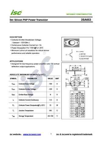
isc Silicon PNP Power Transistor 2SA653 DESCRIPTION Collector-Emitter Breakdown Voltage- V = -120V(Min.) (BR)CEO Contunuous Collector Current I = -1A C Power Dissipation P = 15W @T = 25 C C Minimum Lot-to-Lot variations for robust device performance and reliable operation APPLICATIONS Designed for low frequency power amplifier color TV vertical deflection output appl... See More ⇒
9.9. Size:189K inchange semiconductor
2sa657.pdf
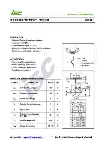
isc Silicon PNP Power Transistor 2SA657 DESCRIPTION Collector-Emitter Breakdown Voltage- V = -80V(Min.) (BR)CEO Complement to Type 2SC520 Minimum Lot-to-Lot variations for robust device performance and reliable operation APPLICATIONS Power amplifier applications. Power switching applications. DC-DC converter applications. Regulator applications. ABSOLUTE MAXIMUM RAT... See More ⇒
Detailed specifications: 2SA642, 2SA643, 2SA645, 2SA646, 2SA647, 2SA648, 2SA649, 2SA65, 2SC5198, 2SA651, 2SA652, 2SA653, 2SA653A, 2SA656, 2SA656A, 2SA657, 2SA657A
Keywords - 2SA650 pdf specs
2SA650 cross reference
2SA650 equivalent finder
2SA650 pdf lookup
2SA650 substitution
2SA650 replacement
