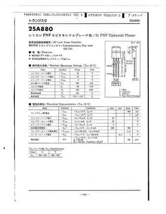
2SA880 Specs and Replacement
Type Designator: 2SA880
Material of Transistor: Si
Polarity: PNP
Absolute Maximum Ratings
Maximum Collector Power Dissipation (Pc): 0.15 W
Maximum Collector-Base Voltage |Vcb|: 35 V
Maximum Collector-Emitter Voltage |Vce|: 35 V
Maximum Emitter-Base Voltage |Veb|: 5 V
Maximum Collector Current |Ic max|: 0.05 A
Max. Operating Junction Temperature (Tj): 125 °C
Electrical Characteristics
Transition Frequency (ft): 120 MHz
Collector Capacitance (Cc): 8 pF
Forward Current Transfer Ratio (hFE), MIN: 260
Noise Figure, dB: -
Package: PAN2
- BJT ⓘ Cross-Reference Search
2SA880 datasheet
9.2. Size:63K panasonic
2sa885.pdf 
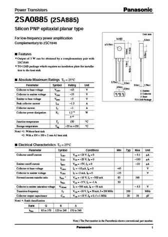
Power Transistors 2SA0885 (2SA885) 2SA0885 (2SA885) 2SA0885 (2SA885) 2SA0885 (2SA885) 2SA0885 (2SA885) Silicon PNP epitaxial planar type Unit mm For low-frequency power amplification 8.0+0.5 0.1 3.2 0.2 Complementary to 2SC1846 3.16 0.1 Features Output of 3 W can be obtained by a complementary pair with 2SC1846 TO-126B package which requires no insulation plat... See More ⇒
9.4. Size:94K panasonic
2sa886.pdf
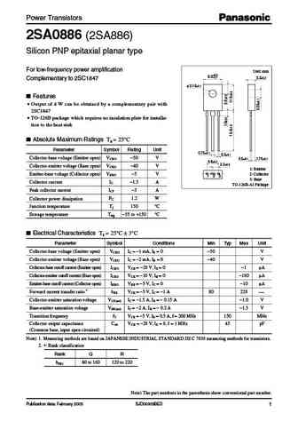
Power Transistors 2SA0886 (2SA886) Silicon PNP epitaxial planar type For low-frequency power amplification Unit mm 8.0+0.5 0.1 3.2 0.2 Complementary to 2SC1847 3.16 0.1 Features Output of 4 W can be obtained by a complementary pair with 2SC1847 TO-126B package which requires no insulation plate for installa- tion to the heat sink Absolute Maximum Ratings ... See More ⇒
9.6. Size:201K jmnic
2sa885.pdf
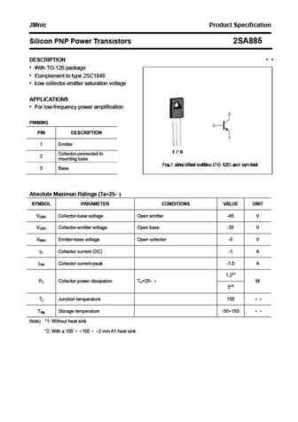
JMnic Product Specification Silicon PNP Power Transistors 2SA885 DESCRIPTION With TO-126 package Complement to type 2SC1846 Low collector-emitter saturation voltage APPLICATIONS For low-frequency power amplification PINNING PIN DESCRIPTION 1 Emitter Collector;connected to 2 mounting base 3 Base Absolute Maximun Ratings (Ta=25 ) SYMBOL PARAMETER CONDITIO... See More ⇒
9.7. Size:97K jmnic
2sa882.pdf
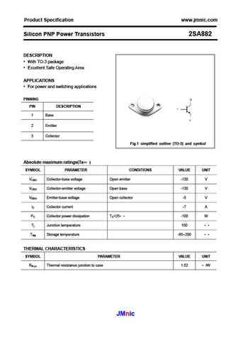
Product Specification www.jmnic.com Silicon PNP Power Transistors 2SA882 DESCRIPTION With TO-3 package Excellent Safe Operating Area APPLICATIONS For power and switching applications PINNING PIN DESCRIPTION 1 Base 2 Emitter 3 Collector Fig.1 simplified outline (TO-3) and symbol Absolute maximum ratings(Ta= ) SYMBOL PARAMETER CONDITIONS VALUE UNIT VCBO Collector... See More ⇒
9.8. Size:169K jmnic
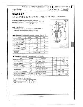
2sa887.pdf
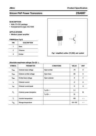
JMnic Product Specification Silicon PNP Power Transistors 2SA887 DESCRIPTION With TO-202 package Complement to type 2SC1848 APPLICATIONS Medium power amplifier PINNING(see Fig.2) PIN DESCRIPTION 1 Base 2 Collector Fig.1 simplified outline (TO-202) and symbol 3 Emitter Absolute maximum ratings (Ta=25 ) SYMBOL PARAMETER CONDITIONS VALUE UNIT VCBO Collector-base vo... See More ⇒
9.9. Size:193K jmnic
2sa886.pdf
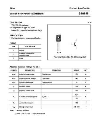
JMnic Product Specification Silicon PNP Power Transistors 2SA886 DESCRIPTION With TO-126 package Complement to type 2SC1847 Low collector-emitter saturation voltage APPLICATIONS For low-frequency power amplification PINNING PIN DESCRIPTION 1 Emitter Collector;connected to 2 mounting base 3 Base Absolute Maximun Ratings (Ta=25 ) SYMBOL PARAMETER CONDITIO... See More ⇒
9.10. Size:174K china
2sa885 3ca885.pdf
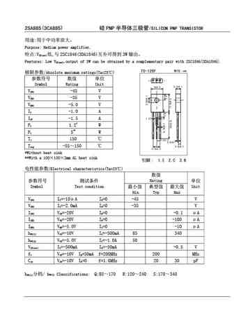
2SA885(3CA885) PNP /SILICON PNP TRANSISTOR Purpose Medium power amplifier. V , 2SC1846(3DA1846) 3W CE(sat) Features Low V ,output of 3W can be obtained by a complementary pair with 2SC1846(3DA1846). CE(sat) /Absolute maximum ratings(Ta=25 ) Symbo... See More ⇒
9.11. Size:229K inchange semiconductor
2sa885.pdf
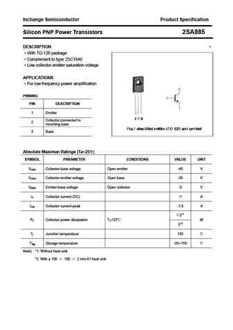
Inchange Semiconductor Product Specification Silicon PNP Power Transistors 2SA885 DESCRIPTION With TO-126 package Complement to type 2SC1846 Low collector-emitter saturation voltage APPLICATIONS For low-frequency power amplification PINNING PIN DESCRIPTION 1 Emitter Collector;connected to 2 mounting base 3 Base Absolute Maximun Ratings (Ta=25 ) SYMBOL P... See More ⇒
9.12. Size:192K inchange semiconductor
2sa882.pdf
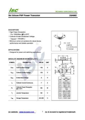
isc Silicon PNP Power Transistor 2SA882 DESCRIPTION High Power Dissipation- P = 100W(Max.)@T =25 C C Collector-Emitter Breakdown Voltage- V = -130V(Min.) (BR)CEO Minimum Lot-to-Lot variations for robust device performance and reliable operation APPLICATIONS Designed for power and switching applications. ABSOLUTE MAXIMUM RATINGS(T =25 ) a SYMBOL PARAMETER VALUE UNI... See More ⇒
9.13. Size:183K inchange semiconductor
2sa887.pdf
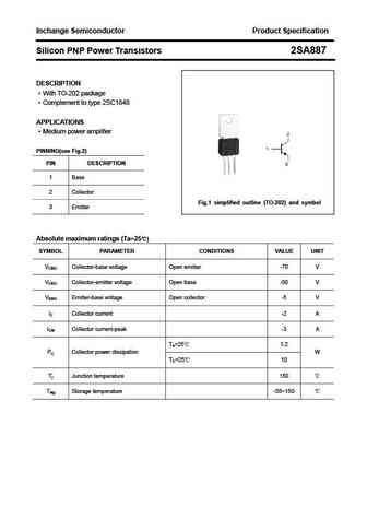
Inchange Semiconductor Product Specification Silicon PNP Power Transistors 2SA887 DESCRIPTION With TO-202 package Complement to type 2SC1848 APPLICATIONS Medium power amplifier PINNING(see Fig.2) PIN DESCRIPTION 1 Base 2 Collector Fig.1 simplified outline (TO-202) and symbol 3 Emitter Absolute maximum ratings (Ta=25 ) SYMBOL PARAMETER CONDITIONS VALUE UNIT VCBO ... See More ⇒
9.14. Size:222K inchange semiconductor
2sa886.pdf
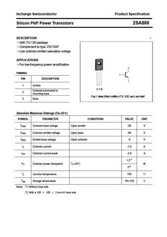
Inchange Semiconductor Product Specification Silicon PNP Power Transistors 2SA886 DESCRIPTION With TO-126 package Complement to type 2SC1847 Low collector-emitter saturation voltage APPLICATIONS For low-frequency power amplification PINNING PIN DESCRIPTION 1 Emitter Collector;connected to 2 mounting base 3 Base Absolute Maximun Ratings (Ta=25 ) SYMBOL P... See More ⇒
Detailed specifications: 2SA876H
, 2SA876HA
, 2SA876HB
, 2SA876HC
, 2SA877
, 2SA878
, 2SA879
, 2SA88
, D882P
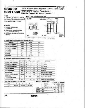
, 2SA881
, 2SA882
, 2SA883
, 2SA884
, 2SA885
, 2SA886
, 2SA887
, 2SA888
.
Keywords - 2SA880 pdf specs
2SA880 cross reference
2SA880 equivalent finder
2SA880 pdf lookup
2SA880 substitution
2SA880 replacement