2SB1059 Specs and Replacement
Type Designator: 2SB1059
Material of Transistor: Si
Polarity: PNP
Absolute Maximum Ratings
Maximum Collector Power Dissipation (Pc): 0.75
W
Maximum Collector-Base Voltage |Vcb|: 70
V
Maximum Emitter-Base Voltage |Veb|: 6
V
Maximum Collector Current |Ic max|: 1
A
Max. Operating Junction Temperature (Tj): 150
°C
Electrical Characteristics
Forward Current Transfer Ratio (hFE), MIN: 200
Noise Figure, dB: -
Package:
TO92
-
BJT ⓘ Cross-Reference Search
2SB1059 datasheet
..1. Size:17K hitachi
2sb1059.pdf 

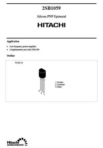
2SB1059 Silicon PNP Epitaxial Application Low frequency power amplifier Complementary pair with 2SD1490 Outline TO-92 (1) 1. Emitter 2. Collector 3. Base 3 2 1 2SB1059 Absolute Maximum Ratings (Ta = 25 C) Item Symbol Ratings Unit Collector to base voltage VCBO 70 V Collector to emitter voltage VCEO 50 V Emitter to base voltage VEBO 6 V Collector current IC ... See More ⇒
8.1. Size:37K panasonic
2sb1050.pdf 

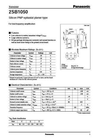
Transistor 2SB1050 Silicon PNP epitaxial planer type For low-frequency amplification Unit mm 6.9 0.1 2.5 0.1 1.5 1.5 R0.9 1.0 Features R0.9 Low collector to emitter saturation voltage VCE(sat). Large collector current IC. M type package allowing easy automatic and manual insertion as well as stand-alone fixing to the printed circuit board. 0.85 0.55 0.1 0.45 0.05 Absolut... See More ⇒
8.2. Size:89K panasonic
2sb1054.pdf 

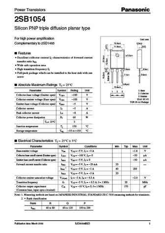
Power Transistors 2SB1054 Silicon PNP triple diffusion planar type For high power amplification Unit mm 15.0 0.3 5.0 0.2 Complementary to 2SD1485 11.0 0.2 (3.2) Features 3.2 0.1 Excellent collector current IC characteristics of forward current transfer ratio hFE Wide safe operation area High transition frequency fT 2.0 0.2 2.0 0.1 Full-pack package wh... See More ⇒
8.3. Size:41K panasonic
2sb1050 e.pdf 

Transistor 2SB1050 Silicon PNP epitaxial planer type For low-frequency amplification Unit mm 6.9 0.1 2.5 0.1 1.5 1.5 R0.9 1.0 Features R0.9 Low collector to emitter saturation voltage VCE(sat). Large collector current IC. M type package allowing easy automatic and manual insertion as well as stand-alone fixing to the printed circuit board. 0.85 0.55 0.1 0.45 0.05 Absolut... See More ⇒
8.5. Size:164K jmnic
2sb1052.pdf 

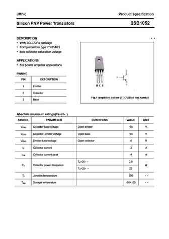
JMnic Product Specification Silicon PNP Power Transistors 2SB1052 DESCRIPTION With TO-220Fa package Complement to type 2SD1480 Low collector saturation voltage APPLICATIONS For power amplifier applications PINNING PIN DESCRIPTION 1 Emitter 2 Collector 3 Base Absolute maximum ratings(Ta=25 ) SYMBOL PARAMETER CONDITIONS VALUE UNIT VCBO Collector-base voltage ... See More ⇒
8.6. Size:161K jmnic
2sb1054.pdf 

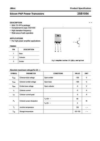
JMnic Product Specification Silicon PNP Power Transistors 2SB1054 DESCRIPTION With TO-3PFa package Complement to type 2SD1485 High transition frequency Wide area of safe operation APPLICATIONS For high power amplifier applications PINNING PIN DESCRIPTION 1 Base 2 Collector 3 Emitter Absolute maximum ratings(Ta=25 ) SYMBOL PARAMETER CONDITIONS VALUE UNIT ... See More ⇒
8.7. Size:160K jmnic
2sb1057.pdf 

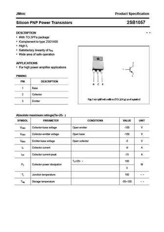
JMnic Product Specification Silicon PNP Power Transistors 2SB1057 DESCRIPTION With TO-3PFa package Complement to type 2SD1488 High fT Satisfactory linearity of hFE Wide area of safe operation APPLICATIONS For high power amplifier applications PINNING PIN DESCRIPTION 1 Base 2 Collector 3 Emitter Absolute maximum ratings(Ta=25 ) SYMBOL PARAMETER CONDIT... See More ⇒
8.8. Size:163K jmnic
2sb1056.pdf 

JMnic Product Specification Silicon PNP Power Transistors 2SB1056 DESCRIPTION With TO-3PFa package Complement to type 2SD1487 High fT Satisfactory linearity of hFE Wide area of safe operation APPLICATIONS For high power amplifier applications PINNING PIN DESCRIPTION 1 Base 2 Collector 3 Emitter Absolute maximum ratings(Ta=25 ) SYMBOL PARAMETER CONDIT... See More ⇒
8.9. Size:214K jmnic
2sb1055.pdf 

JMnic Product Specification Silicon PNP Power Transistors 2SB1055 DESCRIPTION With TO-3PFa package Complement to type 2SD1486 High fT Satisfactory linearity of hFE Wide area of safe operation APPLICATIONS For high power amplifier applications PINNING PIN DESCRIPTION 1 Base 2 Collector 3 Emitter Absolute maximum ratings(Ta=25 ) SYMBOL PARAMETER CONDIT... See More ⇒
8.10. Size:217K inchange semiconductor
2sb1052.pdf 
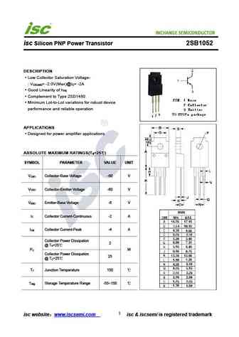
isc Silicon PNP Power Transistor 2SB1052 DESCRIPTION Low Collector Saturation Voltage- V = -2.0V(Max)@I = -2A CE(sat) C Good Linearity of h FE Complement to Type 2SD1480 Minimum Lot-to-Lot variations for robust device performance and reliable operation APPLICATIONS Designed for power amplifier applications ABSOLUTE MAXIMUM RATINGS(T =25 ) a SYMBOL PARAMETER VALUE UNI... See More ⇒
8.11. Size:217K inchange semiconductor
2sb1054.pdf 
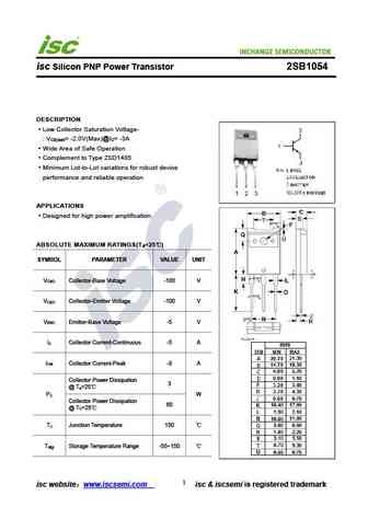
isc Silicon PNP Power Transistor 2SB1054 DESCRIPTION Low Collector Saturation Voltage- V = -2.0V(Max)@I = -3A CE(sat) C Wide Area of Safe Operation Complement to Type 2SD1485 Minimum Lot-to-Lot variations for robust device performance and reliable operation APPLICATIONS Designed for high power amplification. ABSOLUTE MAXIMUM RATINGS(T =25 ) a SYMBOL PARAMETER VALUE UN... See More ⇒
Detailed specifications: 2SB1051
, 2SB1052
, 2SB1053
, 2SB1054
, 2SB1055
, 2SB1056
, 2SB1057
, 2SB1058
, 2SD669A
, 2SB106
, 2SB1060
, 2SB1061
, 2SB1062
, 2SB1063
, 2SB1064
, 2SB1065
, 2SB1066
.
History: PDTA114YT
Keywords - 2SB1059 pdf specs
2SB1059 cross reference
2SB1059 equivalent finder
2SB1059 pdf lookup
2SB1059 substitution
2SB1059 replacement


