2SB1066 Specs and Replacement
Type Designator: 2SB1066
Material of Transistor: Si
Polarity: PNP
Absolute Maximum Ratings
Maximum Collector Power Dissipation (Pc): 1 W
Maximum Collector-Base Voltage |Vcb|: 60 V
Maximum Collector-Emitter Voltage |Vce|: 60 V
Maximum Emitter-Base Voltage |Veb|: 5 V
Maximum Collector Current |Ic max|: 3 A
Max. Operating Junction Temperature (Tj): 150 °C
Electrical Characteristics
Forward Current Transfer Ratio (hFE), MIN: 100
Noise Figure, dB: -
Package: TO92
- BJT ⓘ Cross-Reference Search
2SB1066 datasheet
8.8. Size:78K secos
2sb1068.pdf 
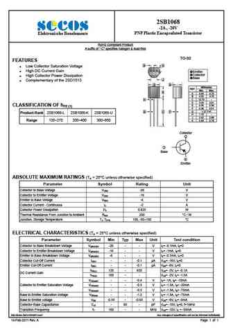
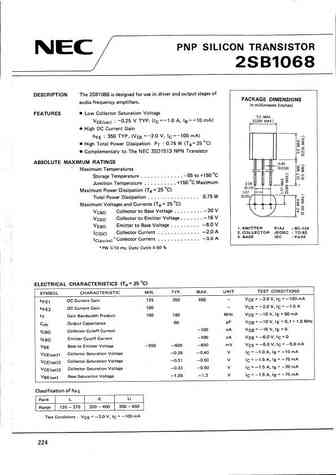
2SB1068 -2A , -20V PNP Plastic Encapsulated Transistor Elektronische Bauelemente RoHS Compliant Product A suffix of -C specifies halogen & lead-free TO-92 FEATURES G H Low Collector Saturation Voltage High DC Current Gain Emitter Collector High Collector Power Dissipation Base J Complementary of the 2SD1513 A D Millimeter REF. Min... See More ⇒
8.9. Size:159K jmnic
2sb1063.pdf
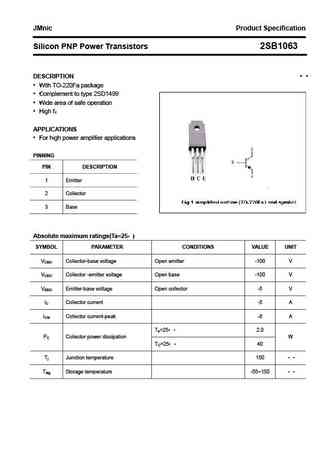
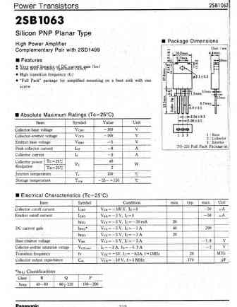
JMnic Product Specification Silicon PNP Power Transistors 2SB1063 DESCRIPTION With TO-220Fa package Complement to type 2SD1499 Wide area of safe operation High fT APPLICATIONS For high power amplifier applications PINNING PIN DESCRIPTION 1 Emitter 2 Collector 3 Base Absolute maximum ratings(Ta=25 ) SYMBOL PARAMETER CONDITIONS VALUE UNIT VCBO Collector-b... See More ⇒
8.10. Size:149K jmnic
2sb1064.pdf
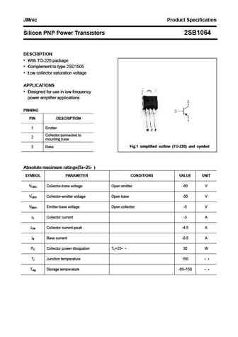
JMnic Product Specification Silicon PNP Power Transistors 2SB1064 DESCRIPTION With TO-220 package Complement to type 2SD1505 Low collector saturation voltage APPLICATIONS Designed for use in low frequency power amplifier applications PINNING PIN DESCRIPTION 1 Emitter Collector;connected to 2 mounting base Fig.1 simplified outline (TO-220) and symbol 3 Base... See More ⇒
8.11. Size:160K jmnic
2sb1069 2sb1069a.pdf
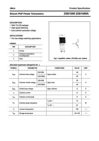
JMnic Product Specification Silicon PNP Power Transistors 2SB1069 2SB1069A DESCRIPTION With TO-220 package High speed switching Low collector saturation voltage APPLICATIONS For low-voltage switching applications PINNING PIN DESCRIPTION 1 Emitter Collector;connected to 2 mounting base Fig.1 simplified outline (TO-220) and symbol 3 Base Absolute maximum ratin... See More ⇒
8.12. Size:154K jmnic
2sb1065.pdf
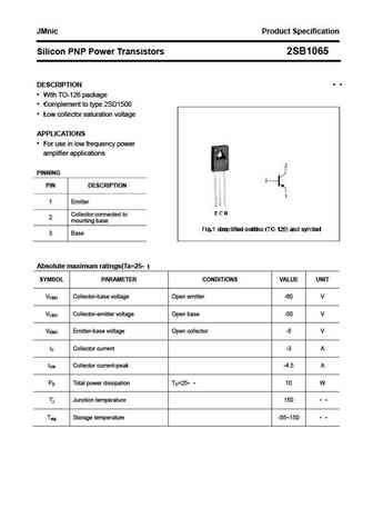
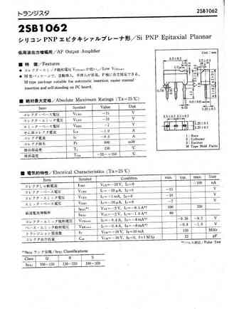
JMnic Product Specification Silicon PNP Power Transistors 2SB1065 DESCRIPTION With TO-126 package Complement to type 2SD1506 Low collector saturation voltage APPLICATIONS For use in low frequency power amplifier applications PINNING PIN DESCRIPTION 1 Emitter Collector;connected to 2 mounting base 3 Base Absolute maximum ratings(Ta=25 ) SYMBOL PARAMET... See More ⇒
8.13. Size:219K inchange semiconductor
2sb1063.pdf
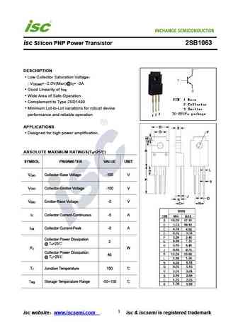
isc Silicon PNP Power Transistor 2SB1063 DESCRIPTION Low Collector Saturation Voltage- V = -2.0V(Max)@I = -3A CE(sat) C Good Linearity of h FE Wide Area of Safe Operation Complement to Type 2SD1499 Minimum Lot-to-Lot variations for robust device performance and reliable operation APPLICATIONS Designed for high power amplification. ABSOLUTE MAXIMUM RATINGS(T =25 ) a... See More ⇒
8.14. Size:217K inchange semiconductor
2sb1064.pdf
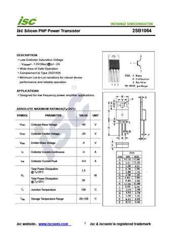
isc Silicon PNP Power Transistor 2SB1064 DESCRIPTION Low Collector Saturation Voltage V = -1.0V(Max)@I = -2A CE(sat) C Wide Area of Safe Operation Complement to Type 2SD1505 Minimum Lot-to-Lot variations for robust device performance and reliable operation APPLICATIONS Designed for low frequency power amplifier applications. ABSOLUTE MAXIMUM RATINGS(T =25 ) a SYMBOL P... See More ⇒
8.15. Size:125K inchange semiconductor
2sb1069 2sb1069a.pdf
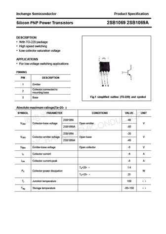
Inchange Semiconductor Product Specification Silicon PNP Power Transistors 2SB1069 2SB1069A DESCRIPTION With TO-220 package High speed switching Low collector saturation voltage APPLICATIONS For low-voltage switching applications PINNING PIN DESCRIPTION 1 Emitter Collector;connected to 2 mounting base Fig.1 simplified outline (TO-220) and symbol 3 Base Absol... See More ⇒
8.16. Size:215K inchange semiconductor
2sb1065.pdf
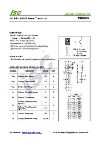
isc Silicon PNP Power Transistor 2SB1065 DESCRIPTION Collector Saturation Voltage Low V = -1.0V(Max)@I = -2A CE(sat) C Wide Area of Safe Operation Complement to Type 2SD1506 Minimum Lot-to-Lot variations for robust device performance and reliable operation APPLICATIONS Designed for low frequency power amplifier applications. ABSOLUTE MAXIMUM RATINGS(T =25 ) a SYMB... See More ⇒
8.17. Size:216K inchange semiconductor
2sb1069.pdf
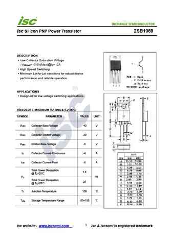
isc Silicon PNP Power Transistor 2SB1069 DESCRIPTION Low Collector Saturation Voltage V = -0.5V(Max)@I = -2A CE(sat) C High Speed Switching Minimum Lot-to-Lot variations for robust device performance and reliable operation APPLICATIONS Designed for low voltage switching applications. ABSOLUTE MAXIMUM RATINGS(T =25 ) a SYMBOL PARAMETER VALUE UNIT V Collector-Base Voltage... See More ⇒
Detailed specifications: 2SB1059
, 2SB106
, 2SB1060
, 2SB1061
, 2SB1062
, 2SB1063
, 2SB1064
, 2SB1065
, 2SC2383
, 2SB1067
, 2SB1068
, 2SB1069
, 2SB107
, 2SB1070
, 2SB1071
, 2SB1072
, 2SB1072L
.
Keywords - 2SB1066 pdf specs
2SB1066 cross reference
2SB1066 equivalent finder
2SB1066 pdf lookup
2SB1066 substitution
2SB1066 replacement