8050 Datasheet, Equivalent, Cross Reference Search
Type Designator: 8050
Material of Transistor: Si
Polarity: NPN
Maximum Collector Power Dissipation (Pc): 1 W
Maximum Collector-Base Voltage |Vcb|: 40 V
Maximum Collector-Emitter Voltage |Vce|: 25 V
Maximum Emitter-Base Voltage |Veb|: 6 V
Maximum Collector Current |Ic max|: 1.5 A
Max. Operating Junction Temperature (Tj): 150 °C
Transition Frequency (ft): 100 MHz
Collector Capacitance (Cc): 9 pF
Forward Current Transfer Ratio (hFE), MIN: 85
Noise Figure, dB: -
Package: TO92
8050 Transistor Equivalent Substitute - Cross-Reference Search
8050 Datasheet (PDF)
8050.pdf


8050 Rev.F Mar.-2016 DATA SHEET / Descriptions TO-92 NPN Silicon NPN transistor in a TO-92 Plastic Package. / Features P ,I , 8550 C CHigh PC and IC, complementary pair with 8550. / Applications 2W 2W output amplifier of portable radios in class B push-pull operation.
8050.pdf


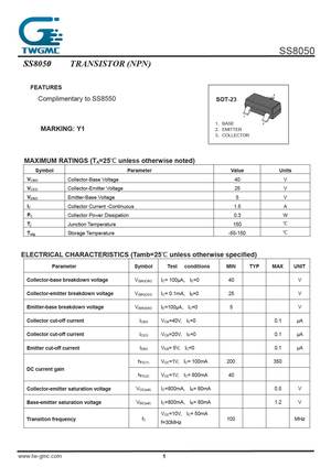
isc Silicon NPN Power Transistor 8050DESCRIPTIONWith SOT-23 packagingHigh collector-base voltageLow saturation voltageMinimum Lot-to-Lot variations for robust deviceperformance and reliable operationAPPLICATIONSAudio output stage and converters/inverters circuitsABSOLUTE MAXIMUM RATINGS(Ta=25)SYMBOL PARAMETER VALUE UNITV Collector-Base Voltage 40 VCBOV Col
cd8050b cd8050c cd8050d.pdf


Continental Device India Pvt. LimitedAn IATF 16949, ISO9001 and ISO 14001 Certified CompanyNPN SILICON PLANAR TRANSISTORS CD8050TO-92Leaded PackageRoHS compliantABSOLUTE MAXIMUM RATINGS (Ta = 25 OC)DESCRIPTION SYMBOL VALUE UNITCollector -Base Voltage VCBO 40 VCollector -Emitter Voltage VCEO 25 VEmitter Base Voltage VEBO 6 VCollector Current IC 2 ACollector Power Dissipat
tpc8050-h.pdf


TPC8050-H TOSHIBA Field Effect Transistor Silicon N-Channel MOS Type (U-MOS-H) TPC8050-H Switching Regulator Applications Motor Drive Applications Unit: mmDC-DC Converter Applications Small footprint due to a small and thin package High-speed switching Small gate charge: QSW = 9.2 nC (typ.) Low drain-source ON-resistance: RDS (ON) = 9.3 m (typ.)
tpca8050-h.pdf


TPCA8050-H TOSHIBA Field Effect Transistor Silicon N-Channel MOS Type (U-MOS-H) TPCA8050-H Switching Regulator Applications Unit: mmMotor Drive Applications 1.27 0.4 0.1 8 0.05 M A DC-DC Converter Applications 5 0.15 0.05 Small footprint due to a small and thin package High-speed switching40.595 Small gate charge: QSW = 10 nC (typ.) 1A
fdms8050.pdf


August 2014FDMS8050N-Channel PowerTrench MOSFET 30 V, 200 A, 0.65 mFeatures General DescriptionThis N-Channel MOSFET has been designed specifically to Max rDS(on) = 0.65 m at VGS = 10 V, ID = 55 Aimprove the overall efficiency and to minimize switch node Max rDS(on) = 0.9 m at VGS = 4.5 V, ID = 47 Aringing of DC/DC converters using either synchronous or Advanced P
fdms8050et30.pdf


January 2015FDMS8050ET30N-Channel PowerTrench MOSFET30 V, 423 A, 0.65 mFeatures General DescriptionThis N-Channel MOSFET has been designed specifically to Extended TJ rating to 175Cimprove the overall efficiency and to minimize switch node Max rDS(on) = 0.65 m at VGS = 10 V, ID = 55 Aringing of DC/DC converters using either synchronous or conventional switching PWM
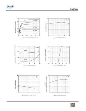
ss8050.pdf


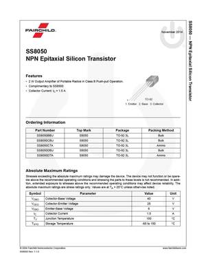
July 2010SS8050NPN Epitaxial Silicon TransistorFeatures 2W Output Amplifier of Portable Radios in Class B Push-pull Operation. Complimentary to SS8550 Collector Current: IC=1.5A Collector Power Dissipation: PC=2W (TC=25C)TO-9211. Emitter 2. Base 3. CollectorAbsolute Maximum Ratings Ta = 25C unless otherwise notedSymbol Parameter Value UnitsVCBO Collecto
ss8050.pdf


SS8050 NPN EPITAXIAL SILICON TRANSISTOR2W OUTPUT AMPLIFIER OF PORTABLETO-92RADIOS IN CLASSB PUSH-PULL OPERATION. Complimentary to SS8550 Collector Current IC=1.5A Collector Dissipation:PC=2W (TC=25 )ABSOLUTE MAXIMUM RATINGS (T =25 )A Characteristic Symbol Rating UnitCollector-Base Voltage VCBO 40 VCollector-Emitter Voltage VCEO 25 VEmitter-Base Voltage VEBO 6
mmss8050-h.pdf


MCCMMSS8050-LTM Micro Commercial Components20736 Marilla Street ChatsworthMicro Commercial ComponentsMMSS8050-HCA 91311Phone: (818) 701-4933Fax: (818) 701-4939Features SOT-23 Plastic-Encapsulate TransistorsNPN Silicon Capable of 0.625Watts(Tamb=25OC) of Power Dissipation. Collector-current 1.5APlastic-Encapsulate Collector-base Voltage 40V Operat
mms8050-l.pdf


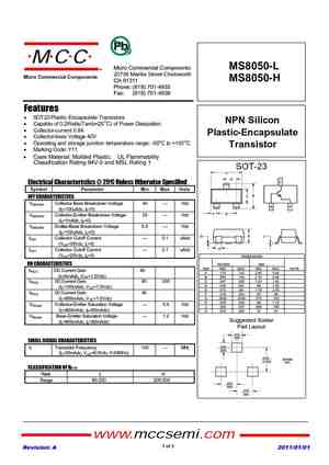
MCCMMS8050-LMicro Commercial ComponentsTM20736 Marilla Street ChatsworthMicro Commercial ComponentsCA 91311MMS8050-HPhone: (818) 701-4933Fax: (818) 701-4939Features SOT-23 Plastic-Encapsulate TransistorsNPN Silicon Capable of 0.3Watts(Tamb=25OC) of Power Dissipation. Collector-current 0.5APlastic-Encapsulate Collector-base Voltage 40V Operating
s8050b s8050c s8050d.pdf


MCCMicro Commercial ComponentsTMS8050-B20736 Marilla Street ChatsworthMicro Commercial ComponentsCA 91311S8050-CPhone: (818) 701-4933Fax: (818) 701-4939 S8050-DFeatures TO-92 Plastic-Encapsulate Transistors Capable of 0.625Watts(Tamb=25OC) of Power Dissipation.NPN Silicon Collector-current 0.5A Collector-base Voltage 40VTransistors Operating an
m8050-d.pdf


MCCMicro Commercial ComponentsTMM8050-C20736 Marilla Street ChatsworthMicro Commercial ComponentsCA 91311M8050-DPhone: (818) 701-4933Fax: (818) 701-4939Features TO-92 Plastic-Encapsulate TransistorsNPN Silicon Capable of 0.625Watts(Tamb=25OC) of Power Dissipation. Collector-current 0.8APlastic-Encapsulate Collector-base Voltage 40V Operating an
mmss8050-l mmss8050-h.pdf
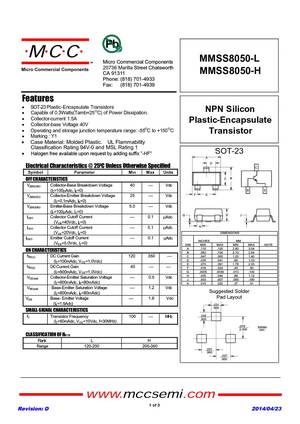

MCCMMSS8050-LTM Micro Commercial Components20736 Marilla Street ChatsworthMicro Commercial ComponentsMMSS8050-HCA 91311Phone: (818) 701-4933Fax: (818) 701-4939Features SOT-23 Plastic-Encapsulate TransistorsNPN Silicon Capable of 0.3Watts(Tamb=25OC) of Power Dissipation. Collector-current 1.5APlastic-Encapsulate Collector-base Voltage 40V Operatin
8050ss-d 8050ss-c.pdf


MCCMicro Commercial ComponentsTM8050SS-C20736 Marilla Street ChatsworthMicro Commercial ComponentsCA 913118050SS-DPhone: (818) 701-4933Fax: (818) 701-4939Features TO-92 Plastic-Encapsulate Transistors Capable of 1.0Watts(Tamb=25OC) of Power Dissipation.NPN Silicon Collector-current 1.5A Collector-base Voltage 40VTransistors Operating and storag
pxt8050-c-d-d3.pdf


PXT8050-CMCCMicro Commercial ComponentsTMPXT8050-D20736 Marilla Street ChatsworthMicro Commercial ComponentsCA 91311PXT8050-D3Phone: (818) 701-4933Fax: (818) 701-4939Features Halogen free available upon request by adding suffix "-HF" Epoxy meets UL 94 V-0 flammability ratingNPN Silicon Moisture Sensitivity Level 1 Marking:Y1 Plastic-Encapsulate
m8050-c.pdf


MCCMicro Commercial ComponentsTMM8050-C20736 Marilla Street ChatsworthMicro Commercial ComponentsCA 91311M8050-DPhone: (818) 701-4933Fax: (818) 701-4939Features TO-92 Plastic-Encapsulate TransistorsNPN Silicon Capable of 0.625Watts(Tamb=25OC) of Power Dissipation. Collector-current 0.8APlastic-Encapsulate Collector-base Voltage 40V Operating an
mms8050-h.pdf


MCCMMS8050-LMicro Commercial ComponentsTM20736 Marilla Street ChatsworthMicro Commercial ComponentsCA 91311MMS8050-HPhone: (818) 701-4933Fax: (818) 701-4939Features SOT-23 Plastic-Encapsulate TransistorsNPN Silicon Capable of 0.3Watts(Tamb=25OC) of Power Dissipation. Collector-current 0.5APlastic-Encapsulate Collector-base Voltage 40V Operating
ms8050-l.pdf

MCCMicro Commercial Components MS8050-LTM20736 Marilla Street ChatsworthMicro Commercial ComponentsMS8050-HCA 91311Phone: (818) 701-4933Fax: (818) 701-4939Features SOT-23 Plastic-Encapsulate TransistorsNPN Silicon Capable of 0.2Watts(Tamb=25OC) of Power Dissipation. Collector-current 0.8APlastic-Encapsulate Collector-base Voltage 40V Operating an
ms8050-h.pdf


MCCMicro Commercial Components MS8050-LTM20736 Marilla Street ChatsworthMicro Commercial ComponentsMS8050-HCA 91311Phone: (818) 701-4933Fax: (818) 701-4939Features SOT-23 Plastic-Encapsulate TransistorsNPN Silicon Capable of 0.2Watts(Tamb=25OC) of Power Dissipation. Collector-current 0.8APlastic-Encapsulate Collector-base Voltage 40V Operating an
mmss8050-l.pdf


MCCMMSS8050-LTM Micro Commercial Components20736 Marilla Street ChatsworthMicro Commercial ComponentsMMSS8050-HCA 91311Phone: (818) 701-4933Fax: (818) 701-4939Features SOT-23 Plastic-Encapsulate TransistorsNPN Silicon Capable of 0.625Watts(Tamb=25OC) of Power Dissipation. Collector-current 1.5APlastic-Encapsulate Collector-base Voltage 40V Operat
mmss8050w-h-j-l.pdf


MMSS8050W-LMCCTM Micro Commercial Components20736 Marilla Street ChatsworthMicro Commercial Components MMSS8050W-HCA 91311Phone: (818) 701-4933MMSS8050W-JFax: (818) 701-4939Features SOT-323 Plastic-Encapsulate TransistorsNPN Silicon Capable of 0.2 Watts(Tamb=25OC) of Power Dissipation. Collector-current 1.5APlastic-Encapsulate Collector-base Voltage 4
mms8050.pdf


MMS8050Features Halogen Free Available Upon Request By Adding Suffix "-HF" Moisture Sensitivity Level 1NPN Silicon Epoxy Meets UL 94 V-0 Flammability Rating Lead Free Finish/RoHS Compliant ("P" Suffix Designates RoHSPlastic-EncapsulateCompliant. See Ordering Information)Maximum Ratings @ 25C Unless Otherwise SpecifiedTransistor Operating Junction Tempera
ss8050-c-d.pdf

MCCMicro Commercial ComponentsTMSS8050-C20736 Marilla Street ChatsworthMicro Commercial ComponentsCA 91311SS8050-DPhone: (818) 701-4933Fax: (818) 701-4939Features TO-92 Plastic-Encapsulate Transistors Capable of 1.0Watts(Tamb=25OC) of Power Dissipation.NPN Silicon Collector-current 1.5A Collector-base Voltage 40VTransistors Operating and storag
fdms8050.pdf


Is Now Part ofTo learn more about ON Semiconductor, please visit our website at www.onsemi.comPlease note: As part of the Fairchild Semiconductor integration, some of the Fairchild orderable part numbers will need to change in order to meet ON Semiconductors system requirements. Since the ON Semiconductor product management systems do not have the ability to manage part nomenclatur
ss8050.pdf
Is Now Part ofTo learn more about ON Semiconductor, please visit our website at www.onsemi.comPlease note: As part of the Fairchild Semiconductor integration, some of the Fairchild orderable part numbers will need to change in order to meet ON Semiconductors system requirements. Since the ON Semiconductor product management systems do not have the ability to manage part nomenclatur
he8050l.pdf


UTC HE8050 NPN EPITAXIAL SILICON TRANSISTORLOW VOLTAGE HIGH CURRENTSMALL SIGNAL NPN TRANSISTORDESCRIPTION The UTC HE8050 is a low voltage high current smallsignal NPN transistor, designed for Class B push-pull 2Waudio amplifier for portable radio and general purposeapplications.1FEATURES*Collector current up to 1.5A*Collector-Emitter voltage up to 25 V*Complimentary to U
s8050.pdf


UNISONIC TECHNOLOGIES CO., LTD S8050 NPN SILICON TRANSISTOR LOW VOLTAGE HIGH CURRENT SMALL SIGNAL NPN TRANSISTOR DESCRIPTION The UTC S8050 is a low voltage high current small signal 1NPN transistor, designed for Class B push-pull audio amplifier TO-92and general purpose applications. FEATURES * Collector current up to 700mA * Collector-Emitter voltage up to 20 V
he8050.pdf


UNISONIC TECHNOLOGIES CO., LTD HE8050 NPN SILICON TRANSISTOR LOW VOLTAGE HIGH CURRENT SMALL SIGNAL NPN TRANSISTOR DESCRIPTION The UTC HE8050 is a low voltage high current small signal NPN transistor, designed for Class B push-pull 2W audio amplifier for portable radio and general purpose applications. FEATURES *Collector current up to 1.5A *Collector-Emitter voltag
8050s.pdf


UNISONIC TECHNOLOGIES CO., LTD 8050S NPN SILICON TRANSISTOR LOW VOLTAGE HIGH CURRENT SMALL SIGNAL NPN TRANSISTOR DESCRIPTION The UTC 8050S is a low voltage high current small signal NPN transistor, designed for Class B push-pull audio amplifier and general purpose applications. FEATURES *Collector current up to 700mA *Collector-Emitter voltage up to 20V * Complem
mmdt8050s.pdf


UNISONIC TECHNOLOGIES CO., LTD MMDT8050S Preliminary NPN EPITAXIAL SILICON TRANSISTOR LOW VCESAT NPN EPITAXIAL PLANAR TRANSISTOR DESCRIPTION The UTC MMDT8050S is a Dual NPN epitaxial planar transistor. It has low VCE(sat) performance, and the transistor elements are independent, eliminating interference. FEATURES * Low VCE(sat), VCE(sat)=40mV (typ.)@IC / IB = 50mA / 2.5mA
utc8050s.pdf


UTC 8050S NPN EPITAXIAL SILICON TRANSISTORLOW VOLTAGE HIGH CURRENTSMALL SIGNAL NPNTRANSISTORDESCRIPTIONThe UTC8050S is a low voltage high current small signalNPN transistor, designed for Class B push-pull audioamplifier and general purpose applications. FEATURES*Collector current up to 800mA*Collector-Emitter voltage up to 20 VTO-92*Complementary to UTC 8550S 1:EMITTER
sps8050.pdf


SPS8050Semiconductor Semiconductor NPN Silicon TransistorFeatures Low saturation medium current application Extremely low collector saturation voltage Suitable for low voltage large current drivers High DC current gain and large current capability Low on resistance : RON=0.6(Max.) (IB=1mA) Ordering Information Type NO. Marking Package Code S
sts8050.pdf


STS8050NPN Silicon TransistorDescriptions PIN Connection High current application C Radio in class B push-pull operation BFeature E Complementary pair with STS8550 TO-92 Ordering Information Type NO. Marking Package Code STS8050 STS8050 TO-92 Absolute Maximum Ratings (Ta=25C) Characteristic Symbol Rating UnitCollector-base voltage VCBO 30 VC
av8050s.pdf


@vic AV8050S NPN EPITAXIAL SILICON TRANSISTOR LOW VOLTAGE HIGH CURRENT SMALL SIGNAL NPN TRANSISTOR DESCRIPTION 3The @vic AV8050S is a low voltage high current small signal 1NPN transistor, designed for Class B push-pull audio amplifier and general purpose applications. 2FEATURES *Collector current up to 700mA *Collector-Emitter voltage up to 20 V *Complementary to @v
s8050.pdf


S8050NPN SiliconElektronische BauelementePlastic-Encapsulate TransistorsRoHS Compliant Product A suffix of "-C" specifies halogen & lead-freeSOT-23FEATURESDim Min MaxCollector3A 2.800 3.040Complimentary to S8550B 1.200 1.4001Base C 0.890 1.1102Collector Current: IC=0.5AEmitter D 0.370 0.500G 1.780 2.040AH 0.013 0.100LJ 0.085 0.1773K 0.450 0.600
s8050t.pdf


S8050T NPN Silicon General Purpose Transistor Elektronische Bauelemente RoHS Compliant Product A suffix of -C specifies halogen and lead free TO-92FEATURES 4.55 0.2 3.5 0.2 (1.27 Typ.) Complimentary to S8550T 1.25 0.2 Collector Current: IC = 0.5 A 1 2 32.54 0.11: Emitter2: Base3: Collector0.080.43 0.070.46 0.1ABSOLUTE MAXIMUM RATINGS at Ta = 25C
ss8050w.pdf


SS8050WNPN SiliconElektronische BauelementeGeneral Purpose TransistorRoHS Compliant ProductSOT-323FEATURESCollectorDim Min Max33A 1.800 2.200Power dissipation11 B 1.150 1.3502 BasePCM : 0.2 WC 0.800 1.000Collector CurrentD 0.300 0.4002ICM : 1.5 A A G 1.200 1.400EmitterLH 0.000 0.100Collector-base voltageJ 0.100 0.2503V(BR)CBO : 40 VSTo
ss8050t.pdf


SS8050TNPN SiliconElektronische Bauelemente General Purpose TransistorRoHS Compliant ProductA suffix of "-C" specifies halogen & lead-freeTO-92FEATURESPower dissipationPCM : 1 WCollector CurrentICM : 1.5 A1Collector-base voltage 23V(BR)CBO : 40 V12 3Operating & storage junction temperature1O OTj, Tstg : - 55 C ~ + 150 C1. EMITTER22. BASS3 . COLLEC
ss8050.pdf


SS8050 NPN Silicon General Purpose Transistor Elektronische Bauelemente RoHS Compliant Product A suffix of -C specifies halogen & lead-free SOT-23FEATURES AL Complimentary to SS8550 33Top View Power Dissipation C B11 2PCM : 0.3W 2K E Collector Current ICM : 1.5A DCollector H J Collector - Base Voltage F GV(BR)CBO : 40V
8050sst.pdf


8050SST 1.5A , 40V NPN Plastic Encapsulated Transistor Elektronische Bauelemente RoHS Compliant Product A suffix of -C specifies halogen & lead-free TO-92 FEATURES General Purpose Switching and Amplification. G HEmitter Collector Base JCLASSIFICATION OF hFE (1) A DMillimeterProduct-Rank 8050SST-B 8050SST-C 8050SST-DREF.B Min. Max.A 4.40
m8050.pdf


M8050 40V, 0.8A, 200mW NPN Plastic Encapsulate Transistor Elektronische Bauelemente RoHS Compliant Product A suffix of -C specifies halogen & lead-free SOT-23 FEATURES A Power dissipation L33Top View C BMARKING 11 2Product Marking Code2K EM8050 Y11DH JF GPACKAGE INFORMATION Millimeter MillimeterPackage MPQ Leader Size REF. REF. Min.
cn8050 cn8550 c d.pdf


Continental Device India LimitedAn ISO/TS 16949, ISO 9001 and ISO 14001 Certified CompanySILICON PLANAR EPITAXIAL TRANSISTORS CN8050 NPNCN8550 PNPTO-92Plastic PackageCBEABSOLUTE MAXIMUM RATINGSDESCRIPTION SYMBOL VALUE UNITSVCEOCollector Emitter Voltage 25 VVCBOCollector Base Voltage 40 VVEBOEmitter Base Voltage 6.0 VICCollector Current 800 mAICMPeak Colle
cmbt8050.pdf


Continental Device India LimitedAn ISO/TS 16949, ISO 9001 and ISO 14001 Certified CompanyNPN SILICON PLANAR EPITAXIAL TRANSISTOR CMBT8050 PIN CONFIGURATION (NPN)1 = BASESOT-232 = EMITTER3 = COLLECTOR3Formed SMD Package12ABSOLUTE MAXIMUM RATINGS DESCRIPTION SYMBOL VALUE UNITSVCBOCollector Base Voltage 30 VVCEOCollector Emitter Voltage 25 VEmitter Base Voltage
s8050.pdf


JIANGSU CHANGJIANG ELECTRONICS TECHNOLOGY CO., LTD TO-92 Plastic-Encapsulate Transistors TO-92 S8050 TRANSISTOR (NPN) FEATURES 1.EMITTER Complimentary to S8550 Collector current: IC=0.5A 2.BASE MAXIMUM RATINGS (Ta=25 unless otherwise noted) 3.COLLECTOR Symbol ParameterValue UnitVCBO Collector-Base Voltage 40 V VCEO Collector-Emitter Voltage 25 V VEBO Emit
pxt8050.pdf


JIANGSU CHANGJIANG ELECTRONICS TECHNOLOGY CO., LTD SOT-89-3L Plastic-Encapsulate Transistors SOT-89-3L PXT8050 TRANSISTOR (NPN) FEATURES Compliment to PXT8550 1. BASE MARKING: Y1 2. COLLECTOR MAXIMUM RATINGS (Ta=25 unless otherwise noted) 3. EMITTER Symbol Parameter Value UnitVCBO Collector-Base Voltage 40 VVCEO Collector-Emitter Voltage 25 VVEBO Emitter-Base V
m8050s.pdf

JIANGSU CHANGJIANG ELECTRONICS TECHNOLOGY CO., LTD TO-92 Plastic-Encapsulate Transistors TO-92 M8050S TRANSISTOR (NPN) 1.EMITTER FEATURES Power Dissipation 2. COLLECTOR3. BASEMAXIMUM RATINGS (Ta=25 unless otherwise noted) Symbol Parameter Value UnitVCBO Collector-Base Voltage 40 V VCEO Collector-Emitter Voltage 25 V VEBO Emitter-Base Voltage 6 V IC Collector Curr
8050ss.pdf


JIANGSU CHANGJIANG ELECTRONICS TECHNOLOGY CO., LTD TO-92 Plastic-Encapsulate Transistors 8050SS TRANSISTOR (NPN) FEATURES TO 92 General Purpose Switching and Amplification. 1. EMITTER 2. COLLECTOR 3. BASE Equivalent Circuit 8050SS=Device code 8050SS Solid dot=Green molding compound device, Z if none,the normal device Z=Rank of hFEXXX=Code1
8050s.pdf


JIANGSU CHANGJIANG ELECTRONICS TECHNOLOGY CO., LTD TO-92 Plastic-Encapsulate Transistors JC TTO-92 8050S TRANSISTOR (NPN) FEATURES 1.EMITTER Complimentary to 8550S 2.COLLECTOR Collector Current: IC=0.5A 3.BASEMAXIMUM RATINGS (Ta=25 unless otherwise noted) Symbol ParameterValue UnitVCBO Collector-Base Voltage 40 V VCEO Collector-Emitter Voltage 25 V VEBO
ss8050.pdf


JIANGSU CHANGJIANG ELECTRONICS TECHNOLOGY CO., LTD TO-92 Plastic-Encapsulate Transistors TO-92 SS8050 TRANSISTOR (NPN) 1. EMITTER FEATURES 2. BASE Power Dissipation 3. COLLECTOR PCM : 1 W (TA=25.) : 2 W (TC=25.) MAXIMUM RATINGS (Ta=25 unless otherwise noted) Symbol Parameter Value UnitVCBO Collector-Base Voltage 40 VVCEO Collector-Emitter Voltage 25 VVEB
m8050.pdf


JIANGSU CHANGJIANG ELECTRONICS TECHNOLOGY CO., LTD TO-92 Plastic-Encapsulate Transistors TO-92 M8050 TRANSISTOR (NPN) 1.EMITTER FEATURES Power Dissipation 2. BASE 3. COLLECTOR Equivalent Circuit M8050M8050=Device code Solid dot = Green molding compound device, Z if none, the normal device Z=Range of hFEXXX=Code 11ORDERING INFORMATION Pa
mps8050sc.pdf


SEMICONDUCTOR MPS8050SCTECHNICAL DATA EPITAXIAL PLANAR NPN TRANSISTORHIGH CURRENT APPLICATION. FEATUREComplementary to MPS8550SC.MAXIMUM RATING (Ta=25)CHARACTERISTIC SYMBOL RATING UNITVCBOCollector-Base Voltage 40 VVCEOCollector-Emitter Voltage 25 VVEBOEmitter-Base Voltage 5 VICCollector Current 1,200 mAPC *Collector Power Dissipation 350 mWTjJunction Te
ktc8050a.pdf


SEMICONDUCTOR KTC8050ATECHNICAL DATA EPITAXIAL PLANAR NPN TRANSISTORHIGH CURRENT APPLICATION. B CFEATUREComplementary to KTC8550A.N DIM MILLIMETERSA 4.70 MAXEKB 4.80 MAXMAXIMUM RATING (Ta=25) GC 3.70 MAXDD 0.45CHARACTERISTIC SYMBOL RATING UNITE 1.00F 1.27VCBOCollector-Base Voltage 35 VG 0.85H 0.45VCEOCollector-Emitter Voltage 30 V_HJ 14.0
ktc8050s.pdf


SEMICONDUCTOR KTC8050STECHNICAL DATA EPITAXIAL PLANAR NPN TRANSISTORHIGH CURRENT APPLICATION. FEATUREEL B LComplementary to KTC8550S.DIM MILLIMETERS_A 2.93 0.20+B 1.30+0.20/-0.15C 1.30 MAX23 D 0.45+0.15/-0.05E 2.40+0.30/-0.20MAXIMUM RATING (Ta=25 )1G 1.90H 0.95CHARACTERISTIC SYMBOL RATING UNITJ 0.13+0.10/-0.05K 0.00 ~ 0.10VCBOCollector-Base Voltag
mps8050s.pdf


SEMICONDUCTOR MPS8050STECHNICAL DATA EPITAXIAL PLANAR NPN TRANSISTORHIGH CURRENT APPLICATION. FEATUREEL B LComplementary to MPS8550S.DIM MILLIMETERS_+A 2.93 0.20B 1.30+0.20/-0.15C 1.30 MAX23 D 0.40+0.15/-0.05E 2.40+0.30/-0.201G 1.90MAXIMUM RATING (Ta=25)H 0.95J 0.13+0.10/-0.05CHARACTERISTIC SYMBOL RATING UNITK 0.00 ~ 0.10QL 0.55VCBO P PCo
mps8050.pdf


SEMICONDUCTOR MPS8050TECHNICAL DATA EPITAXIAL PLANAR NPN TRANSISTORHIGH CURRENT APPLICATION.B CFEATURE Complementary to MPS8550.N DIM MILLIMETERSA 4.70 MAXEKB 4.80 MAXGMAXIMUM RATING (Ta=25 )C 3.70 MAXDD 0.45CHARACTERISTIC SYMBOL RATING UNITE 1.00F 1.27VCBOCollector-Base Voltage 40 VG 0.85H 0.45VCEOCollector-Emitter Voltage 25 V _HJ 14.00 + 0.


c8050b c8050c c8050d.pdf


TransistorsC8050www.DataSheet4U.comwww.DataSheet4U.com
s8050.pdf


S8 050TRANSISTOR(NPN)SOT-23 FEATURES Complimentary to S8550 1. BASE Collector Current: IC=0.8A 2. EMITTER 3. COLLECTOR MARKING: J3Y MAXIMUM RATINGS (TA=25 unless otherwise noted) Symbol Parameter Value UnitsVCBO Collector-Base Voltage 40 V VCEO Collector-Emitter Voltage 25 V VEBO Emitter-Base Voltage 5 V IC Collector Current -Continuous 0.8 A PC Collector
pxt8050.pdf


PXT8 050TRANSISTOR(NPN)SOT-89 FEATURES Compliment to PXT8550 1. BASE MARKING: Y1 2. COLLECTOR MAXIMUM RATINGS (TA=25 unless otherwise noted) 3. EMITTER Symbol Parameter Value UnitsVCBO Collector-Base Voltage 40 VVCEO Collector-Emitter Voltage 25 VVEBO Emitter-Base Voltage 6 VIC Collector Current -Continuous 1.5 A PC Collector Power dissipation 0.5 W TJ Junctio
ss8050.pdf


SS8 050SOT-23 TRANSISTOR(NPN)FEATURES 1. BASE High Collector Current 2. EMITTER Complementary to SS8550 3. COLLECTOR MARKING: Y1MAXIMUM RATINGS (TA=25 unless otherwise noted) Symbol Parameter Value UnitsVCBO Collector-Base Voltage 40 V VCEO Collector-Emitter Voltage 25 V VEBO Emitter-Base Voltage 5 V IC Collector Current -Continuous 1.5 A PC Collector
m8050.pdf


M8050TRANSISTOR(NPN)SOT-23 FEATURES Power dissipation 1. BASE 2. EMITTER MARKING: Y11 3. COLLECTOR MAXIMUM RATINGS (TA=25 unless otherwise noted) Symbol Parameter Value UnitsVCBO Collector-Base Voltage 40 V VCEO Collector-Emitter Voltage 25 V VEBO Emitter-Base Voltage 6 V IC Collector Current -Continuous 0.8 APC Collector Power Dissipation 0.2 W Tj Junction
s8050.pdf


Guilin Strong Micro-Electronics Co.,Ltd.Guilin Strong Micro-Electronics Co.,Ltd.Guilin Strong Micro-Electronics Co.,Ltd.GM8050FEATURESFEATURES FEATURESLow Frequency Power Amplifier Suitable for Driver Stage of Small Motor Complementary to GM8550 GM8550 (Ta=25 )


s8050a.pdf


Guilin Strong Micro-Electronics Co.,Ltd.Guilin Strong Micro-Electronics Co.,Ltd.Guilin Strong Micro-Electronics Co.,Ltd.GM8050FEATURESFEATURES FEATURESLow Frequency Power Amplifier Suitable for Driver Stage of Small Motor Complementary to GM8550 GM8550 (Ta=25 )
ss8050.pdf


Guilin Strong Micro-Electronics Co.,Ltd.Guilin Strong Micro-Electronics Co.,Ltd.Guilin Strong Micro-Electronics Co.,Ltd.GM8050FEATURESFEATURES FEATURESLow Frequency Power Amplifier Suitable for Driver Stage of Small Motor Complementary to GM8550 GM8550 (Ta=25 )
m8050.pdf


Guilin Strong Micro-Electronics Co.,Ltd.Guilin Strong Micro-Electronics Co.,Ltd.Guilin Strong Micro-Electronics Co.,Ltd.GM8050FEATURESFEATURES FEATURESLow Frequency Power Amplifier Suitable for Driver Stage of Small Motor Complementary to GM8550 GM8550 (Ta=25 )
s8050.pdf


S8050 Silicon Epitaxial Planar TransistorFEATURES A SOT-23 High Collector Current.(IC= 500mA). Dim Min MaxA 2.70 3.10E Complementary To S8550. B 1.10 1.50K BC 1.0 Typical Excellent HFE Linearity. D 0.4 TypicalE 0.35 0.48J High total power dissipation.(PC=300mW). DG 1.80 2.00GH 0.02 0.1J 0.1 TypicalHAPPLICATIONS K 2.20 2.60CAll Dimensions in mm
s8050 to-92.pdf


S8050(NPN)TO-92 Bipolar Transistors 1. EMITTER TO-92 2. BASE 3. COLLECTOR Features Complimentary to S8550 Collector current: IC=0.5A MAXIMUM RATINGS (TA=25 unless otherwise noted) Symbol ParameterValue UnitsVCBO Collector-Base Voltage 40 V VCEO Collector-Emitter Voltage 25 V VEBO Emitter-Base Voltage 5 V IC Collector Current -Continuous 0.5 A Dimensions in
pxt8050.pdf


PXT8050 SOT-89 Transistor(NPN)1. BASE 2. COLLECTOR 3. EMITTER SOT-894.6B4.41.61.8Features 1.41.4 Compliment to PXT8550 2.64.252.43.75 0.8MARKING: Y1 MIN0.530.400.480.442x)0.13 BMAXIMUM RATINGS (TA=25 unless otherwise noted) 0.35 0.371.53.0Symbol Parameter Value UnitsDimensions in inches and (millimeters)VCBO Collector-Base
s8050 sot-23.pdf


S8050 SOT-23 Transistor(NPN)SOT-231. BASE 2. EMITTER 3. COLLECTOR Features Complimentary to S8550 Collector Current: IC=0.5A MARKING: J3Y Dimensions in inches and (millimeters)MAXIMUM RATINGS (TA=25 unless otherwise noted) Symbol Parameter Value UnitsVCBO Collector-Base Voltage 40 V VCEO Collector-Emitter Voltage 25 V VEBO Emitter-Base Voltage 5 V IC Collect
m8050 sot-23.pdf


M8050 SOT-23 Transistor(NPN)SOT-231. BASE 2. EMITTER 3. COLLECTOR Features Power dissipation MARKING: Y11 Dimensions in inches and (millimeters)MAXIMUM RATINGS (TA=25 unless otherwise noted) Symbol Parameter Value UnitsVCBO Collector-Base Voltage 40 V VCEO Collector-Emitter Voltage 25 V VEBO Emitter-Base Voltage 6 V IC Collector Current -Continuous 0.8 APC
8050s to-92.pdf


8050S(NPN) TO-92 Bipolar TransistorsTO-92 1. EMITTER 4.455.21 2. COLLECTOR 3. BASE 4.322.92 5.33MINFeaturesComplimentary to 8550S 3.43Collector current: IC=0.5A MIN2.412.67MAXIMUM RATINGS (TA=25 unless otherwise noted) Symbol Parameter3.18Value Units2.034.192.67VCBO Collector-Base Voltage 40 V 1.141.40VCEO Collector-Emitter Volt
ss8050 to-92.pdf


SS8050(NPN)TO-92 Bipolar TransistorsTO-92 1. EMITTER 2. BASE 3. COLLECTOR Features Power dissipation PCM : 1 W (TA=25) : 2 W (TC=25) MAXIMUM RATINGS (TA=25 unless otherwise noted) Symbol Parameter Value UnitsVCBO Collector-Base Voltage 40 VVCEO Collector-Emitter Voltage 25 VDimensions in inches and (millimeters)VEBO Emitter-Base Voltage 5 VIC C
ss8050.pdf


SS8050(NPN)TO-92 Bipolar TransistorsTO-921.EMITTER2. BASE3. COLLECTORFeatures Power dissipation PCM : 1 W (TA=25) : 2 W (TC=25) MAXIMUM RATINGS (TA=25 unless otherwise noted) Symbol Parameter Value UnitsVCBO Collector-Base Voltage 40 VVCEO Collector-Emitter Voltage 25 VDimensions in inches and (millimeters)VEBO Emitter-Base Voltage 5 VIC Collector
m8050 to-92.pdf


M8050(NPN)TO-92 TransistorsTO-92 1. EMITTER 2. BASE 3. COLLECTOR Features Power dissipation MAXIMUM RATINGS (TA=25 unless otherwise noted) Symbol Parameter Value UnitsVCBO Collector-Base Voltage 40 V VCEO Collector-Emitter Voltage 25 V VEBO Emitter-Base Voltage 6 V IC Collector Current -Continuous 800 mA PC Collector Power Dissipation 625 mW Dimensions i
ss8050 sot-23.pdf


SS8050 SOT-23 Transistor(NPN)SOT-231. BASE 2. EMITTER 3. COLLECTOR FeaturesComplimentary to SS8550 MARKING: Y1 Dimensions in inches and (millimeters)MAXIMUM RATINGS (TA=25 unless otherwise noted) Symbol Parameter Value UnitsVCBO Collector-Base Voltage 40 V VCEO Collector-Emitter Voltage 25 V VEBO Emitter-Base Voltage 5 V IC Collector Current -Continuous 1.5 A
m8050lt1.pdf


M8050LT1NPN General Purpose Transistors3P b Lead(Pb)-Free12SOT-23ValueVCEO 25405.0 8003002.44170.125100 40 5.01000.15u35u4.0 0.15WEITRON1/4 15-Jul-10http://www.weitron.com.twM8050LT1ELECTRICAL CHARACTERISTICS (TA=25 C unless otherwise noted) (Countinued)CharacteristicsSymbol Max UnitMMinON CHARACTERISTICSDC Current Gain-
s8050.pdf


S8050NPN General Purpose TransistorsTO-921. EMITTER122. BASE33. COLLECTORABSOLUTE MAXIMUM RATINGS (Ta=25 C)Rating SymbolValue UnitCollector-Emitter Voltage VCEO 25 VdcCollector-Base Voltage VCBO 40VdcEmitter-Base VOltage VEBO5.0 VdcCollector Current IC500 mAdcPD 0.625Total Device Dissipation T =25 C WAJunction Temperature T 150j CStorage, Temper
ss8050.pdf


SS8050NPN General Purpose TransistorsTO-92P b Lead(Pb)-Free1. EMITTER122. BASE33. COLLECTORMAXIMUM RATINGS(TA=25C unless otherwise noted)Rating Symbol Value UnitVCBO40Collector-Base Voltage VCollector-Emitter Voltage VCEO 25VVEBOEmitter-Base Voltage 5 VCollector Current-ContinuousIC A1.5Total Device Dissipation TA=25CPD W1.0TJ,TstgJunction
ss8050lt1.pdf

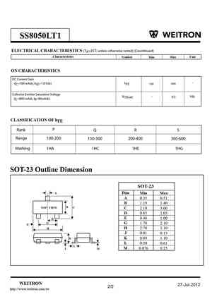
SS8050LT1NPN General Purpose Transistors3P b Lead(Pb)-Free12SOT-23ValueVCEO 25405.015003002.44170.12540100 5.0100u0.15350.15 u4.0WEITRON 27-Jul-20121/2http://www.weitron.com.twSS8050LT1ELECTRICAL CHARACTERISTICS (TA=25 C unless otherwise noted) (Countinued)CharacteristicsSymbol Max UnitMinON CHARACTERISTICSDC Current Gai
8050plt1 8050qlt1 8050rlt1.pdf


FM120-M WILLASTHRU8050xLT1General Purpose TransistorsFM1200-M 1.0A SURFACE MOUNT SCHOTTKY BARRIER RECTIFIERS -20V- 200VSOD-123 PACKAGE Pb Free ProductPackage outlineFeatures Batch process design, excellent power dissipation offers better reverse leakage current and thermal resistance.SOD-123H Low profile surface mounted application in order toNPN Silicon
8050hxlt1.pdf


FM120-M WILLAS8050HxLT1THRUGeneral Purpose BARRIER RECTIFIERS -20V- 200VTransistorsFM1200-M 1.0A SURFACE MOUNT SCHOTTKYSOD-123 PACKAGE Pb Free ProductPackage outlineFeatures Batch process design, excellent power dissipation offers better reverse leakage current and thermal resistance.SOD-123H Low profile surface mounted application in order toNPN Silicon
8050slt1.pdf


FM120-MWILLAS8050SLT1THRU SOT-23 Plastic-Encapsulate Transistors FM1200-M1.0A SURFACE MOUNT SCHOTTKY BARRIER RECTIFIERS -20V- 200VSOD-123 PACKAGE Pb Free ProdPackage outlineFeatures Batch process design, excellent power dissipation offers better reverse leakage current and thermal resistance.TRANSISTOR (NPN) SOD-123H Low profile surface mounted application i
hmbt8050.pdf


Spec. No. : HE6812 HI-SINCERITY Issued Date : 1992.08.25 Revised Date :2010.10.19 MICROELECTRONICS CORP. Page No. : 1/4 HMBT8050 NPN EPITAXIAL TRANSISTOR Description The HMBT8050 is designed for general purpose amplifier applications. SOT-23 Features High DC Current hFE=150-400 at IC=150mA Complementary to HMBT8550 Absolute Maximum Ratings Maximum Tempera
he8050.pdf


Spec. No. : HE6112HI-SINCERITYIssued Date : 1992.09.30Revised Date : 2004.11.29MICROELECTRONICS CORP.Page No. : 1/4HE8050NPN EPITAXIAL PLANAR TRANSISTORDescriptionThe HE8050 is designed for use in 2W output amplifier of portable radios in class Bpush-pull operation.TO-92Features High total power dissipation (PT: 2W, TC=25C) High collector current (IC: 1.5A)
ha8050s.pdf


Spec. No. : HE6116HI-SINCERITYIssued Date : 1997.09.08Revised Date : 2005.01.20MICROELECTRONICS CORP.Page No. : 1/5HA8050SNPN EPITAXIAL PLANAR TRANSISTORDescriptionThe HA8550S is designed for general purpose amplifier applications.TO-92Features High DC Current Gain (hFE=100~500 at IC=150mA) Complementary to HA8550SAbsolute Maximum Ratings Maximum Temperatu
he8050s.pdf


Spec. No. : HE6110HI-SINCERITYIssued Date : 1992.09.30Revised Date : 2004.07.26MICROELECTRONICS CORP.Page No. : 1/5HE8050SNPN EPITAXIAL PLANAR TRANSISTORDescriptionThe HE8050S is designed for general purpose amplifier applications.TO-92Absolute Maximum Ratings Maximum TemperaturesStorage Temperature ...................................................................
ha8050.pdf


Spec. No. : HE6107HI-SINCERITYIssued Date : 1998.09.05Revised Date : 2004.11.29MICROELECTRONICS CORP.Page No. : 1/5HA8050NPN EPITAXIAL PLANAR TRANSISTORDescriptionThe HA8050 is designed for use in 2W output amplifier of portable radios in class Bpush-pull operation.TO-92Features High total power dissipation (PT: 2W, TC=25C) High collector current (IC: 1.5A)
s8050.pdf


Shenzhen Tuofeng Semiconductor Technology Co., Ltd TO-92 Plastic-Encapsulate Transistors S8050 TRANSISTOR (NPN) TO-92 FEATURES 1. EMITTER Power dissipation 2. BASE PCM: 0.625 W (Tamb=25) 3. COLLECTOR Collector current ICM: 0.5 A Collector-base voltage 1 2 3 V(BR)CBO: 40 V Operating and storage junction temperature range TJ, Tstg: -55 to +150
s8050lt1.pdf


Shenzhen Tuofeng Semiconductor Technology Co., Ltd SOT-23 Plastic-Encapsulate Transistors SOT-23 S8050LT1 TRANSISTOR (NPN) 1. BASE 2. EMITTER 3. COLLECTOR FEATURES Power dissipation 2. 4 PCM: 0.3 W (Tamb=25) 1. 3 Collector current ICM: 0.5 A Collector-base voltage V(BR)CBO: 40 V Unit: mm Operating and storage junction temperature range TJ, Tstg:
ss8050.pdf


Shenzhen Tuofeng Semiconductor Technology Co., Ltd TO-92 Plastic-Encapsulate Transistors SS8050 TRANSISTOR (NPN) TO-92 FEATURES 1. EMITTER 2. BASE Power dissipation PCM : 1 W (TA=25) 3. COLLECTOR : 2 W (TC=25) 1 2 3 MAXIMUM RATINGS* TA=25 unless otherwise noted Symbol Parameter Value UnitsVCBO Collector-Base Voltage 40 VVCEO Collector-Emitter Volt
ss8050lt1.pdf

Shenzhen Tuofeng Semiconductor Technology Co., Ltd SOT-23 Plastic-Encapsulate Transistors SS8050LT1 TRANSISTOR (NPN) SOT-23 1. BASE 2. EMITTER FEATURES 3. COLLECTOR Power dissipation 2. 4 PCM: 0.3 W ( Tamb=25) 1. 3 Collector current ICM: 1.5 A Collector-base voltage V(BR)CBO: 25 V Operating and storage junction temperature range Unit: mm TJ, Tst
btn8050ba3.pdf


Spec. No. : C223A3-B Issued Date : 2004.02.18 CYStech Electronics Corp.Revised Date : 2012.10.03 Page No. : 1/8 General Purpose NPN Epitaxial Planar Transistor BTN8050BA3Description The BTN8050BA3 is designed for use in output amplifier of portable radios in class B push pull operation. Features High collector current , I = 1.5A C Low V CE(sat) Complementa
btn8050a3.pdf


Spec. No. : C223A3 Issued Date : 2003.07.30 CYStech Electronics Corp.Revised Date : 2013.05.21 Page No. : 1/5 General Purpose NPN Epitaxial Planar Transistor BTN8050A3Description The BTN8050A3 is designed for use in output amplifier of portable radios in class B push pull operation. Features High collector current , I = 1.5A C Low V CE(sat) Complementary t
s8050 sot-23 8325.pdf


ShenZhen CanSheng Industry Development Co.,Ltd. www.szcansheng.com SOT-23 Plastic-Encapsulate Transistors S8050 TRANSISTOR (NPN) FEATURES Complimentary to S8550 Collector current:Ic=0.5A MARKING:J3Y MAXIMUM RATINGS (TA=25 unless otherwise noted) Symbol Parameter Value Units
s8050 to-92.pdf


ShenZhen CanSheng Industry Development Co.,Ltd. www.szcansheng.com TO-92 Plastic-Encapsulate Transistors S8050 TRANSISTOR (NPN) FEATURES Complimentary to S8550 Collector current:Ic=0.5A MAXIMUM RATINGS (TA=25 unless otherwise noted) Symbol Parameter Value Units VCBO
ss8050 y1 sot-23.pdf


ShenZhen CanSheng Industry Development Co.,Ltd. www.szcansheng.com SOT-23 Plastic-Encapsulate Transistors SS8050 TRANSISTOR (NPN) FEATURES Complimentary to SS8550 MARKING:Y1 MAXIMUM RATINGS (TA=25 unless otherwise noted) Symbol Parameter Value Units VCBO Collector-Base
ss8050.pdf


TO-92 Plastic-Encapsulate TransistorsFEATURESTO-92Power dissipationPCM : 1 W (TA=25) 1.EMITTER: 2 W (TC=25) 2.BASEMAXIMUM RATINGS 3.COLLECTORMAXIMUM RATINGSMAXIMUM RATINGS (TA=25 unless otherwise noted)MAXIMUM RATINGS1 2 3Symbol Parameter Value UnitsSymbol Parameter Value UnitsSymbol Parameter Value UnitsSymbol Parameter Value UnitsVCBO 40 VVCBOVCBO Co
s8050.pdf


S8050 Rev.E Mar.-2016 DATA SHEET / Descriptions TO-92 NPN Silicon NPN transistor in a TO-92 Plastic Package. / Features PC,IC , S8550 High PC and IC, complementary pair with S8550. / Applications Amplifier of portable radios in class B push-pull operation.
8050t.pdf


8050T Rev.E Mar.-2016 DATA SHEET / Descriptions SOT-89 NPN Silicon NPN transistor in a SOT-89 Plastic Package. / Features 8550T Complementary pair with 8550T. / Applications Power amplifier applications. / Equivalent Circuit / Pinning 1 2
8050m.pdf


8050M Rev.E Mar.-2016 DATA SHEET / Descriptions SOT-23 NPN Silicon NPN transistor in a SOT-23 Plastic Package. / Features 8550M Complementary pair with 8550M. / Applications Power amplifier applications. / Equivalent Circuit / Pinning
l8050.pdf


L8050(BR3DA8050K) Rev.C Feb.-2015 DATA SHEET / Descriptions TO-92 NPN Silicon NPN transistor in a TO-92 Plastic Package. / Features PC, IC , L8550(BR3CA8550K) High PC and IC, complementary pair with L8550(BR3CA8550K). / Applications 2W 2W output amplifier of portable radios in cl
stc8050n.pdf


STC8050NSemiconductor Semiconductor NPN Silicon TransistorDescriptions High current application Radio in class B push-pull operation Feature Complementary pair with STA8550N Ordering Information Type NO. Marking Package Code STC8050N STC8050 TO-92N Outline Dimensions unit : mm 4.20~4.402.25 Max.0.52 Max.0.90 Max.1.27 Typ.0.40 Max.1 2 33.55
8050w.pdf


8050W(BR3DA8050W) Rev.C Feb.-2015 DATA SHEET / Descriptions SOT-323 NPN Silicon NPN transistor in a SOT-323 Plastic Package. / Features 8550W(BR3CA8550W)Complementary pair with 8550W(BR3CA8550W). / Applications Power amplifier applications. / Equivalent Circui
s8050a.pdf


S8050A(BR3DG8050AK) Rev.C Feb.-2015 DATA SHEET / Descriptions TO-92 NPN Silicon NPN transistor in a TO-92 Plastic Package. / Features PC, IC , S8550A(BR3CG8550AK) High PC and IC, complementary pair with S8550A(BR3CG8550AK). / Applications Amplifier of portable radios in class B pu
s8050m.pdf


S8050M Rev.F Apr.-2017 DATA SHEET / Descriptions SOT-23 NPN Silicon NPN transistor in a SOT-23 Plastic Package. / Features S8550M Complementary pair with S8550M. / Applications Power amplifier applications. / Equivalent Circuit / Pinnin
s8050mg.pdf


S8050MG Rev.F Apr.-2017 DATA SHEET / Descriptions SOT-23 NPN Silicon NPN transistor in a SOT-23 Plastic Package. / Features S8550MG Complementary pair with S8550MG.HF Product. / Applications Power amplifier applications. / Equivalent Ci
s8050w.pdf


S8050W(BR3DG8050W) Rev.C Feb.-2015 DATA SHEET / Descriptions SOT-323 NPN Silicon NPN transistor in a SOT-323 Plastic Package. / Features S8550W(BR3CG8550W)Complementary pair with S8550W(BR3CG8550W). / Applications Power amplifier applications. / Equivalent Cir
l8050m.pdf


L8050M Rev.C Feb.-2015 DATA SHEET / Descriptions SOT-23 NPN Silicon NPN transistor in a SOT-23 Plastic Package. / Features L8550M Complementary pair with L8550M. / Applications Power amplifier applications. / Equivalent Circuit / Pinning 3 2

st8050-1.5a.pdf


ST 8050 (1.5A) NPN Silicon Epitaxial Planar Transistor for switching and amplifier applications. Especially suitable for AF-driver stages and low power output stages. On special request, these transistors can be manufactured in different pin configurations. 1. Emitter 2. Base 3. Collector TO-92 Plastic Package Absolute Maximum Ratings (Ta = 25) Parameter Symbol Value Uni
st8050-2a.pdf


ST 8050 (2A) NPN Silicon Epitaxial Planar Transistor for switching and amplifier applications. Especially suitable for AF-driver stages and low power output stages. The transistor is subdivided into two groups C and D according to its DC current gain. 1. Emitter 2. Base 3. Collector TO-92 Plastic Package OAbsolute Maximum Ratings (Ta = 25 C) Parameter Symbol Value Unit C
mmbt8050cw mmbt8050dw.pdf


MMBT8050W (1.5A) NPN Silicon Epitaxial Planar Transistor for switching and amplifier applications OAbsolute Maximum Ratings (Ta = 25 C) Parameter Symbol Value UnitCollector Base Voltage VCBO 40 VCollector Emitter Voltage VCEO 25 VEmitter Base Voltage VEBO 5 VPeak Collector Current ICM 1.5 A Total Power Dissipation Ptot 200 mWOJunction Temperature Tj 150 C OStorage Te
8050b 8050c 8050d 8050e.pdf


8050 NPN Silicon Epitaxial Planar Transistor for switching and amplifier applications. Especially suitable for AF-driver stages and low power output stages. The transistor is subdivided into four groups, B, C, D and E, according to its DC current gain. 1. Emitter 2. Base 3. Collector TO-92 Plastic Package OAbsolute Maximum Ratings (Ta = 25 C) Parameter Symbol Value Unit
8050u-c 8050u-d.pdf


8050U NPN Silicon Epitaxial Planar Transistor for switching and amplifier applications. Especially suitable for AF-driver stages and low power output stages. Absolute Maximum Ratings (Ta = 25) Symbol Value UnitParameter Collector Base Voltage VCBO 40 VCollector Emitter Voltage VCEO 25 VEmitter Base Voltage VEBO 6 VCollector Current IC 1.5 APower Dissipation Ptot 625 m
8050c 8050d.pdf


8050 (1.5A) NPN Silicon Epitaxial Planar Transistor for switching and amplifier applications. Especially suitable for AF-driver stages and low power output stages. On special request, these transistors can be manufactured in different pin configurations. 1. Emitter 2. Base 3. Collector TO-92 Plastic Package Absolute Maximum Ratings (Ta = 25) Parameter Symbol Value Unit
l8050hqlt1g.pdf


LESHAN RADIO COMPANY, LTD.General Purpose TransistorsL8050HQLTIGSeriesNPN SiliconS-L8050HQLTIGFEATURESeries High current capacity in compact package.IC =1.5 A.3 Epitaxial planar type. NPN complement: L8050HPb-Free Package is available. 1 S- Prefix for Automotive and Other Applications Requiring Unique Site and Control Change Requirements; AEC-Q101 Qualified and
lh8050qlt1g.pdf


LESHAN RADIO COMPANY, LTD.General Purpose TransistorsLH8050PLT1GSeriesNPN SiliconS-LH8050PLT1GFEATURE Series High current capacity in compact package.IC =1.5A.3 Epitaxial planar type. NPN complement: LH8050 Pb-Free Package is available.1 S- Prefix for Automotive and Other Applications Requiring Unique Site and 2Control Change Requirements; AEC-Q101 Qualified and
lh8050plt1g lh8050plt3g lh8050qlt1g lh8050qlt3g.pdf


LESHAN RADIO COMPANY, LTD.General Purpose TransistorsLH8050PLT1GSeriesNPN SiliconS-LH8050PLT1GFEATURE Series High current capacity in compact package.IC =1.5A.3 Epitaxial planar type. NPN complement: LH8050 Pb-Free Package is available.1 S- Prefix for Automotive and Other Applications Requiring Unique Site and 2Control Change Requirements; AEC-Q101 Qualified and
l8050hplt1g l8050hplt3g l8050hqlt1g l8050hqlt3g l8050hrlt1g l8050hrlt3g l8050hslt1g l8050hslt3g.pdf


LESHAN RADIO COMPANY, LTD.General Purpose TransistorsL8050HQLTIGSeriesNPN SiliconS-L8050HQLTIGFEATURESeries High current capacity in compact package.IC =1.5 A.3 Epitaxial planar type. NPN complement: L8050HPb-Free Package is available. 1 S- Prefix for Automotive and Other Applications Requiring Unique Site and Control Change Requirements; AEC-Q101 Qualified and
l8050hplt1g.pdf


LESHAN RADIO COMPANY, LTD.L8050HQLTIGGeneral Purpose TransistorsSeriesNPN Silicon S-L8050HQLTIGFEATURESeries High current capacity in compact package.IC =1.5 A.3 Epitaxial planar type. NPN complement: L8050H Pb-Free Package is available.1 S- Prefix for Automotive and Other Applications Requiring Unique Site 2and Control Change Requirements; AEC-Q101 Qualified and
l8050hslt1g.pdf


LESHAN RADIO COMPANY, LTD.General Purpose TransistorsL8050HQLTIGNPN SiliconSeriesS-L8050HQLTIGFEATURE High current capacity in compact package.SeriesIC =1.5 A. Epitaxial planar type.3 NPN complement: L8050H Pb-Free Package is available. S- Prefix for Automotive and Other Applications Requiring Unique Site 1and Control Change Requirements; AEC-Q101 Qualified and P
l8050hrlt1g.pdf


LESHAN RADIO COMPANY, LTD.General Purpose TransistorsL8050HQLTIGSeriesNPN SiliconS-L8050HQLTIGFEATURE High current capacity in compact package.SeriesIC =1.5 A. Epitaxial planar type.3 NPN complement: L8050H Pb-Free Package is available. S- Prefix for Automotive and Other Applications Requiring Unique Site 1and Control Change Requirements; AEC-Q101 Qualified and P
lx8050qlt1g.pdf


LESHAN RADIO COMPANY, LTD.General Purpose TransistorsLX8050PLT1GNPN Silicon SeriesS-LX8050PLT1GFEATURESeries High current capacity in compact package.IC = 0.5A. Epitaxial planar type.3 NPN complement: LX8050 Pb-Free Package is available. S- Prefix for Automotive and Other Applications Requiring Unique Site and 1Control Change Requirements; AEC-Q101 Qualified and PPAP
l8050plt1g l8050qlt1g l8050rlt1g l8050slt1g.pdf


LESHAN RADIO COMPANY, LTD.L8050PLT1GGeneral Purpose TransistorsSeriesNPN SiliconS-L8050PLT1GFEATURESeries High current capacity in compact package.IC = 0.8A. Epitaxial planar type. 3 NPN complement: L8050 Pb-Free Package is available.1 S- Prefix for Automotive and Other Applications Requiring Unique Site2and Control Change Requirements; AEC-Q101 Qualified and PPA
l8050hplt1g l8050hqlt1g l8050hrlt1g l8050hslt1g.pdf


LESHAN RADIO COMPANY, LTD.General Purpose TransistorsL8050HQLTIGSeriesNPN SiliconS-L8050HQLTIGFEATURE High current capacity in compact package.SeriesIC =1.5 A. Epitaxial planar type.3 NPN complement: L8050H Pb-Free Package is available. S- Prefix for Automotive and Other Applications Requiring Unique Site 1and Control Change Requirements; AEC-Q101 Qualified and P
l8050qlt1g.pdf


LESHAN RADIO COMPANY, LTD.L8050PLT1GGeneral Purpose TransistorsSeriesNPN SiliconS-L8050PLT1GFEATURESeries High current capacity in compact package.IC = 0.8A. Epitaxial planar type. 3 NPN complement: L8050 Pb-Free Package is available.1 S- Prefix for Automotive and Other Applications Requiring Unique Site2and Control Change Requirements; AEC-Q101 Qualified and PPA
lh8050plt1g lh8050qlt1g.pdf


LESHAN RADIO COMPANY, LTD.General Purpose TransistorsLH8050PLT1GSeriesNPN SiliconS-LH8050PLT1GFEATURE Series High current capacity in compact package.IC =1.5A.3 Epitaxial planar type. NPN complement: LH8050 Pb-Free Package is available.1 S- Prefix for Automotive and Other Applications Requiring Unique Site and 2Control Change Requirements; AEC-Q101 Qualified and
lh8050plt1g.pdf


LESHAN RADIO COMPANY, LTD.General Purpose TransistorsLH8050PLT1GSeriesNPN SiliconS-LH8050PLT1GFEATURE High current capacity in compact package.SeriesIC =1.5A. Epitaxial planar type. NPN complement: LH80503 Pb-Free Package is available. S- Prefix for Automotive and Other Applications Requiring Unique Site and 1Control Change Requirements; AEC-Q101 Qualified and PP
l8050plt1g l8050plt3g l8050qlt1g l8050qlt3g l8050rlt1g l8050rlt3g l8050slt1g l8050slt3g.pdf


LESHAN RADIO COMPANY, LTD.L8050PLT1GGeneral Purpose TransistorsSeriesNPN SiliconS-L8050PLT1GFEATURESeries High current capacity in compact package.IC = 0.8A. Epitaxial planar type. 3 NPN complement: L8050 Pb-Free Package is available.1 S- Prefix for Automotive and Other Applications Requiring Unique Site2and Control Change Requirements; AEC-Q101 Qualified and PPA
l8050plt1g.pdf


LESHAN RADIO COMPANY, LTD.General Purpose TransistorsL8050PLT1GSeriesNPN SiliconS-L8050PLT1GFEATURE Series High current capacity in compact package.IC = 0.8A.3 Epitaxial planar type. NPN complement: L8050 Pb-Free Package is available.1 S- Prefix for Automotive and Other Applications Requiring Unique Site 2and Control Change Requirements; AEC-Q101 Qualified and PP
h8050.pdf


Shantou Huashan Electronic Devices Co.,Ltd. H8050 NPN EPITAXIAL SILICON TRANSISTOR 2W OUTPUT AMPLIFIER OF PORTABLE RADIOS IN CLASS B PUSH-PULL OPERATION. ABSOLUTE MAXIMUM RATINGSTa=25 TstgStorage Temperature -55~150 TO-92 TjJuncttion Temperature150PCCollector Dissipatio
hc8050s.pdf


NPN S I L I C O N T R A N S I S T O R Shantou Huashan Electronic Devices Co.,Ltd. HC8050S APPLICATIONS Audio Frequency Amplifier. ABSOLUTE MAXIMUM RATINGSTa=25 TstgStorage Temperature -55~150 TO-92 TjJuncttion Temperature150PCCollector Dissipation
h8050s.pdf


NPN S I L I C O N T R A N S I S T O R Shantou Huashan Electronic Devices Co.,Ltd. H8050S APPLICATIONS Audio Frequency Amplifier. ABSOLUTE MAXIMUM RATINGSTa=25 TstgStorage Temperature -55~150 TO-92 TjJuncttion Temperature150PCCollector Dissipation
hc8050.pdf


Shantou Huashan Electronic Devices Co.,Ltd. HC8050 NPN EPITAXIAL SILICON TRANSISTOR 2W OUTPUT AMPLIFIER PORTABLE RADIO IN CLASS B PUSH-PULL OPERATION. ABSOLUTE MAXIMUM RATINGSTa=25 TstgStorage Temperature -55~150 TO-92 TjJuncttion Temperature150PCCollector Dissipation
3dg8050.pdf

3DG8050 NPN PCM TA=25 330 mW ICM 300 mA Tjm 175 Tstg -55~150 V(BR)CBO ICB0.1mA 30 V V(BR)CEO ICE0.1mA 25 V V(BR)EBO IEB0.1mA 6.0 V ICBO VCB=20V 0.1 A VBEsat 1.2 V IC=50mA IB=5mA VCEsat 0.5 V VCE=1V hFE 20~100 IC=0.
ftc8050h.pdf


SEMICONDUCTOR FTC8050HTECHNICAL DATA General Purpose Transistors NPN Silicon FEATURE 3 High current capacity in compact package. I C =1.5A. 1 Epitaxial planar type. 2 PNP complement: FTA8550HPb-Free Package is available. SOT23 COLLECTOR DEVICE MARKING AND ORDERING INFORMATION 3 Shipping Device Marking 1 FTC8050H 1FC 3000/Tape&Reel BASE 2 E
ss8050g.pdf


SS8050GPlastic-Encapsulate Transistors Simplified outlineSS8050G TRANSISTOR NPN TO-92Features Power Dissipation 1.EMITTER PCM : 1 W (TA=25.) 2.BASE : 2 W (TC=25.) 3.COLLECTOR123 Maximum Ratings(Ta=25 unless otherwise noted) Symbol Parameter Value UnitVCBO Collector-Base Voltage 40 VVCEO Collector-Emitter Voltage 25 VVEBO Emitter-Base Voltage 5 VIC
s8050g.pdf


S8050GPlastic-Encapsulate Transistors Simplified outlineS8050G TRANSISTOR NPN TO-92Features Power dissipation 1.EMITTER PCM : 0.625 WTamb=25 2. COLLECTOR Collector current ICM : 0.5 A 3.BASE Collector-base voltage 123 V(BR)CBO : 40 V Operating and storage junction temperature range TJTstg: -55 to +150 Electrical Characteristics
f8050hplg.pdf


F8050HPLGPlastic-Encapsulate TransistorsSimplified outlineF8050HPLG TRANSISTOR NPN SOT-23Features Complimentary to F8550HQLG Collector Current: IC=0.5A 1. BASE 2. EMITTER Marking: 1HA3. COLLECTOR Maximum Ratings(Ta=25 unless otherwise noted) Symbol Parameter Value UnitVCBO Collector-Base Voltage 40 V VCEO Collector-Emitter Voltage 25 V VEBO Emitter-
ftc8050.pdf


SEMICONDUCTORFTC8050TECHNICAL DATA TRANSISTOR (NPN) FTC8050B C FEATURES Complimentary to FTA8550 Collector current: IC=0.5ADIM MILLIMETERSA 4.70 MAXEB 4.80 MAXGMAXIMUM RATINGS (Ta=25 unless otherwise noted) C 3.70 MAXDD 0.55 MAXSymbol Parameter Value Unit E 1.00F 1.27G 0.85VCBO Collector-Base Voltage 40 V H 0.45_HJ 14.00 0.50+VCEO Col
f8050hqlg.pdf


F8050HQLGPlastic-Encapsulate TransistorsSimplified outlineF8050HQLG TRANSISTOR NPN SOT-23Features Power dissipation PCM : 0.3 WTamb=25 1. BASE Collector current2. EMITTER ICM : 1.5 A 3. COLLECTOR Collector-base voltage V(BR)CBO : 40 V Operating and storage junction temperature range TJTstg: -55 to +150 Device Mark
kst8050d-50.pdf


SMD Type TransistorsSMD TypeNPN TransistorsKST8050D-50SOT-23Unit: mm+0.12.9 -0.10.4+0.1-0.13Features Collector Current Capability IC=1.2A Collector Emitter Voltage VCEO=50V1 2+0.1+0.050.95 -0.1 0.1-0.01+0.11.9-0.11.Base2.Emitter3.collectorAbsolute Maximum Ratings Ta = 25Parameter Symbol Rating UnitCollector-Base Voltage VCBO 50 VCollec
h8050.pdf


SMD Type TransistorsNPN TransistorsH8050 Features1.70 0.1 Collector Power Dissipation: PC=1W Collector Current: IC=1.5A Comlementary to H85500.42 0.10.46 0.11.Base2.Collector3.Emitter Absolute Maximum Ratings Ta = 25Parameter Symbol Rating UnitCollector-base voltage VCBO 40 VCollector-emitter voltage VCEO 25 VEmitter-base voltage VEBO 5 VC
kst8050.pdf


SMD Type TransistorsSMD TypeNPN TransistorsKST8050SOT-23Unit: mm+0.12.9 -0.10.4+0.1-0.13FeaturesCollector Current: IC=1.5A1 2+0.1+0.050.95 -0.1 0.1-0.01+0.11.9-0.11.Base2.Emitter3.collectorAbsolute Maximum Ratings Ta = 25Parameter Symbol Rating UnitCollector-Base Voltage VCBO 40 VCollector-Emitter Voltage VCEO 25 VEmitter-Base Voltage VEBO 5 V
kst8050m.pdf


SMD TypeSMD Type TransistorsNPN TransistorsKST8050MSOT-23Unit: mm+0.12.9 -0.1+0.10.4-0.13 Features Collector Current: IC=0.8A1 2+0.1+0.050.95 -0.1 0.1 -0.01+0.11.9 -0.11.Base2.Emitter3.collector Absolute Maximum Ratings Ta = 25Parameter Symbol Rating UnitCollector-Base Voltage VCBO 40 VCollector-Emitter Voltage VCEO 25 VEmitter-Bas
kst8050x.pdf


SMD Type TransistorsNPN TransistorsKST8050XSOT-23Unit: mm+0.12.9 -0.1+0.10.4-0.13 Features Collector Power Dissipation: PC=0.3W Collector Current: IC=1.5A1 2+0.1+0.050.95 -0.1 0.1 -0.01+0.11.9 -0.11.Base2.Emitter3.collector Absolute Maximum Ratings Ta = 25Parameter Symbol Rating UnitCollector-Base Voltage VCBO 40 VCollector-Emitte
kst8050d.pdf


SMD Type TransistorsSMD TypeNPN Transistors KST8050DSOT-23Unit: mm+0.12.9 -0.1+0.10.4 -0.13FeaturesCollector Current: IC=1.5A1 2+0.1+0.050.95 -0.1 0.1 -0.01+0.11.9 -0.11.Base2.Emitter3.collectorAbsolute Maximum Ratings Ta = 25Parameter Symbol Rating UnitCollector-Base Voltage VCBO 40 VCollector-Emitter Voltage VCEO 25 VEmitter-Base Voltage VEB
kst8050s.pdf


SMD Type TransistorsSMD TypeNPN TransistorsKST8050SSOT-23Unit: mm2.9+0.1-0.1+0.10.4-0.13FeaturesCollector Current: IC=0.5A1 2+0.1+0.050.95 -0.1 0.1 -0.01+0.11.9 -0.11.Base2.Emitter3.collectorAbsolute Maximum Ratings Ta = 25Parameter Symbol Rating UnitCollector-Base Voltage VCBO 40 VCollector-Emitter Voltage VCEO 25 VEmitter-Base Voltage VEBO 5
mmbt8050d.pdf


MMBT8050DoTRANSISTOR (NPN)FEATURES SOT-23 Complimentary to S8550 Collector Current: IC=0.5A 1BASE 2EMITTER 3COLLECTOR MAXIMUM RATINGS (TA=25 unless otherwise noted) Symbol Parameter Value Units VCBO Collector-Base Voltage 40 V VCEO Collector-Emitter Voltage 25 V VEBO Emitter-Base Voltage 5 V IC Collector Current -Continuous 0.5 A PC Collector Dissipat
cht8050gp.pdf


CHENMKO ENTERPRISE CO.,LTDCHT8050GPSURFACE MOUNTEPITAXIAL TransistorVOLTAGE 20 Volts CURRENT 700 mAmpereFEATURE* Small surface mounting type. (SOT-23)* High DC current . SOT-23CONSTRUCTION(1)* NPN transistors in one package.(3)(2)MARKING( ) ( )* D805 .055 1.40 .028 0.70( ) ( ).047 1.20 .020 0.50* E805( ).103 2.64.086 (2.20)( ).045 1.15C (3)CIR
dmbt8050.pdf


DC COMPONENTS CO., LTD.DMBT8050DISCRETE SEMICONDUCTORSRTECHNICAL SPECIFICATIONS OF NPN EPITAXIAL PLANAR TRANSISTORDescriptionDesigned for general purpose amplifier applications.SOT-23.020(0.50)Pinning.012(0.30)1 = Base 2 = Emitter 3.063(1.60) .108(2.80)3 = Collector.047(1.20) .083(2.10)1 2.045(1.20)Absolute Maximum Ratings(TA=25oC).034(0.90).091(2.30).0
dc8050.pdf

DC COMPONENTS CO., LTD.DC8050DISCRETE SEMICONDUCTORSRTECHNICAL SPECIFICATIONS OF NPN EPITAXIAL PLANAR TRANSISTORDescriptionDesigned for use in 2W output amplifier of portableradios in class B push-pull operation.TO-92Pinning.190(4.83)1 = Emitter.170(4.33)2 = Base2oTyp3 = Collector.190(4.83).170(4.33)2oTypAbsolute Maximum Ratings(TA=25oC).500Characterist
s8050daf.pdf
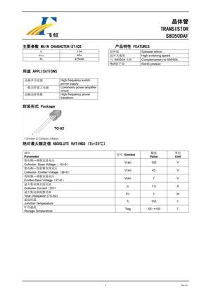

TRANSISTOR S8050DAF MAIN CHARACTERISTICS FEATURES IC 1.5A Epitaxial silicon VCEO 45V High switching speed PC 625mW S8550A Complementary to S8550A RoHS RoHS product APPLICATIONS High frequency switch power supply Commonly power amplifier
s8050sdb.pdf


TRANSISTOR S8050SDB MAIN CHARACTERISTICS FEATURES IC 500mA Epitaxial silicon VCEO 27V High switching speed PC 625mW RoHS RoHS product APPLICATIONS High frequency switch power supply Commonly power amplifier circuit High frequency power
s8050da.pdf


IC 1.5A Epitaxial siliconVCEO 45V High switching speedPC 1W S8550DA Complementary to S8550DARoHS RoHS product High frequency switch power supplyCommonly power amplifier circuitHigh frequency power transform TO-92
s8050d.pdf


TRANSISTOR S8050D MAIN CHARACTERISTICS FEATURES IC 1.5A Epitaxial silicon VCEO 45V High switching speed PC 625mW S8550D Complementary to S8550D RoHS RoHS product APPLICATIONS High frequency switch power supply Commonly power amplifier
3dg8050m.pdf


S8050M(3DG8050M) NPN /SILICON NPN TRANSISTOR :/Purpose: Power amplifier applications. : S8550M(3CG8550M)/Features: Complementary pair with S8550M(3CG8550M). /Absolute maximum ratings(Ta=25) Symbol Rating Unit V 40 V CBO V 25 V CEO V 6.0 V EBO I 800 mA C
pxt8050.pdf


Product specification PLASTIC-ENCAPSULATE TRANSISTORS PXT8050(NPN) FEATURES Commplimentray to PXT8550 Pb Lead-free APPLICATIONS This device is designed as a general purpose amplifier and switching. SOT-89 ORDERING INFORMATION Type No. Marking Package Code PXT8050 8050 SOT-89 : none is for Lead Free package; G is for Halogen Free package. MAX
ss8050.pdf


Product specification NPN Silicon Epitaxial Planar Transistor SS8050 FEATURES Pb Collector Current.(I = 1.5A CLead-free Complementary To SS8550. Collector dissipation:P =300mW(T =25) C CAPPLICATIONS High Collector Current. SOT-23 ORDERING INFORMATION Type No. Marking Package Code SS8050 Y1 SOT-23 : none is for Lead Free package;
gstss8050.pdf

GSTSS8050 NPN General Purpose Transistor Product Description Features This device is designed as a general purpose Collector-Emitter Voltage : 25V amplifier and switch. Collector Current : 1.5A Lead(Pb)-FreePackages & Pin Assignments TO-92 Pin Description1 Emitter 2 Base 3 Collector Marking Information P/N Package Rank Part Marking GSTSS8050F TO-92 (B) / (C) / (
gstss8050lt1.pdf


GSTSS8050LT1 NPN General Purpose Transistor Product Description Features This device is designed as a general purpose Collector-Emitter Voltage : 25V amplifier and switch. Collector-Base Voltage : 40V Collector Current : 1500mA Lead(Pb)-FreePackages & Pin Assignments SOT-23 Pin Description1 Base 2 Emitter 3 Collector Marking Information P/N Package Part Markin
gstm8050lt1.pdf


GSTM8050LT1 NPN General Purpose Transistor Product Description Features This device is designed as a general purpose Collector-Emitter Voltage : 25V amplifier and switch. Collector Current : 800mA Lead(Pb)-FreePackages & Pin Assignments SOT-23 Pin Description1 Base 2 Emitter 3 Collector Marking Information P/N Package Rank Part Marking GSTM8050LT1F SOT-23 P 80P
ks8050l.pdf


KS8050L NPN Silicon Transistor Descriptions PIN Connection High current application Features Complementary pair with KS8550L Ordering Information Type NO. Marking Package Code KK KS8050L SOT-23 Device Code HFE Grade Year& Week Code AUK Dalian SOT-23 Absolute maximum ratings Ta=25C Characteristic Symbol Ratings Unit Colle
k8050s.pdf


K8050S NPN Silicon Transistor 2018.09.07 2018.09.07 2018.09.07 2018.09.07 1 000 2017.11.02 2 001 2018.08.22 3 TAPING 003 2018.09.07 K8050S NPN S
3dg8050a.pdf


S8050A(3DG8050A) NPN /SILICON NPN TRANSISTOR : Purpose: Amplifier of portable radios in class B push-pull operation. :P I , S8550A(3CG8550A) C CFeatures: High P ,I , complementary pair with S8550A(3CG8550A). C C/Absolute maximum ratings(Ta=25) Symbol Rating
pt23t8050.pdf


PT23T8050 Transistor Feature 3 - Collector 1 - Base This device is Pb-Free, Halogen Free/BFR Free and Rohs compliant. 2 - Emitter Mechanical Characteristics Lead finish:100% matte Sn(Tin) Mounting position: Any Qualified max reflow temperature:260 Device meets MSL 1 requirements Pure tin plating: 7 ~ 17 um Pin flatness:3mil Structu
shd280504.pdf


SENSITRON SHD280504SEMICONDUCTORTECHNICAL DATADATA SHEET 4066, REV.-HERMETIC POWER MOSFETN-CHANNELFEATURES: 400 Volt, 0.3 Ohm, 14A MOSFET Low RDS (on) Electrically Equivalent to IRF350 SeriesMAXIMUM RATINGS ALL RATINGS ARE AT TC = 25C UNLESS OTHERWISE SPECIFIED.RATING SYMBOL MIN. TYP. MAX. UNITSGATE TO SOURCE VOLTAGE VGS - - 20VoltsID - - 14 AmpsON-ST
shd280502.pdf


SENSITRON SHD280502SEMICONDUCTORTECHNICAL DATADATA SHEET 4065, REV. -HERMETIC POWER MOSFETN-CHANNELDESCRIPTION: A 100-VOLT, 0.055-OHM MOSFET IN A HERMETIC TO-3 / TO-204AA PACKAGE.MAXIMUM RATINGS ALL RATINGS ARE AT TA = 25C UNLESS OTHERWISE SPECIFIED.RATING SYMBOL MIN. TYP. MAX. UNITSGATE TO SOURCE VOLTAGE VGS - - 20VoltsID - - 38 AmpsCONTINUOUS DRAIN CURRENT @ TC
ss8050-l ss8050-h ss8050-j.pdf


SS8050TRANSISTOR(NPN)SOT-23 1. BASE FEATURES 2. EMITTER Complimentary to SS8550 3. COLLECTOR MAXIMUM RATINGS (TA=25 unless otherwise noted) Symbol Parameter Value UnitsVCBO Collector-Base Voltage 40 V VCEO Collector-Emitter Voltage 25 V VEBO Emitter-Base Voltage 5 V IC Collector Current -Continuous 1.5 A PC Collector Power Dissipation 0.3 W Tj Junction Temperat
s8050b s8050c s8050d.pdf


S8050NPN General Purpose TransistorsTO-921. EMITTER122. BASE33. COLLECTORABSOLUTE MAXIMUM RATINGS (Ta=25 C)Rating SymbolValue UnitCollector-Emitter Voltage VCEO 25 VdcCollector-Base Voltage VCBO 40VdcEmitter-Base VOltage VEBO5.0 VdcCollector Current IC500 mAdcPD 0.625Total Device Dissipation T =25 C WAJunction Temperature T 150j CStorage, Temper
s8050tl s8050th s8050tj.pdf


S8050TNPN TransistorsMarkingMarking J3Y32 1.Base2.Emitter3.Collector1 Simplified outline(SOT-523) Absolute Maximum Ratings Ta = 25Symbol Parameter Value UnitsVCBO Collector-Base Voltage 40 VVCEO Collector-Emitter Voltage 25 VVEBO Emitter-Base Voltage 5 VIC Collector Current -Continuous 0.5 APC Collector Dissipation 0.2 WTj Junction Temperature 150
s8050w-l s8050w-h s8050w-j.pdf


S8050WTRANSISTOR (NPN)FEATURES SOT-323 Complimentary to S8550 WCollector Current: IC=0.5A 1. BASE 2. EMITTER 3. COLLECTOR MARKING: J3Y MAXIMUM RATINGS (TA=25 unless otherwise noted) Symbol Parameter Value UnitsVCBO Collector-Base Voltage 40 VVCEO Collector-Emitter Voltage 25 VVEBO Emitter-Base Voltage 5 VIC Collector Current -Continuous 0.5 APC Collector Diss
ss8050w.pdf


SS8050WNPN Transistors Features3 High Collector Current Complementary to SS8550W21.Base2.Emitter3.Collector1 Simplified outline(SOT-323) Absolute Maximum Ratings Ta = 25Symbol Parameter Value Unit VCBO Collector-Base Voltage 40 V VCEO Collector-Emitter Voltage 25 V VEBO Emitter-Base Voltage 5 V IC Collector Current 1.5 APC Collector Power Dissip
8050c.pdf

SUNROC8050C TRANSISTOR(NPN) MAXIMUM RATINGS(Ta=25 unless otherwise noted) 1. EMITTER Symbol Parameter Value UnitsCollector-Base Voltage 2. BASE VCBO 40 VCollector-Emitter Voltage VCEO 25 V3. COLLECTOR Emitter-Base Voltage VEBO 5 VCollector Current IC 0.5 ACollector Power Dissipation PC 625 mWJunction Temperature Tj 150 Storag Temperature -55150
mmbt8050.pdf


Tel/Fax: +86 (0)769 82827329 Skype: topdiodeEmail: info@topdiode.com Website: www.topdiode.comTel/Fax: +86 (0)769 82827329 Skype: topdiodeEmail: info@topdiode.com Website: www.topdiode.com
s8050l s8050h.pdf


RUMW S8050TRANSISTOR(NPN) SOT-23 FEATURES Complimentary to S8550 1. BASE Collector Current: IC=0.5A 2. EMITTER 3. COLLECTOR MARKING: J3Y MAXIMUM RATINGS (TA=25 unless otherwise noted) Symbol Parameter Value UnitsVCBO Collector-Base Voltage 40 V VCEO Collector-Emitter Voltage 25 V VEBO Emitter-Base Voltage 5 V IC Collector Current -Continuous 0.5 A PC C
ss8050l ss8050h ss8050j.pdf


RUMW UMW SS8050SOT-23 Plastic-Encapsulate TransistorsSOT-23 SS8050 TRANSISTOR (NPN) 1. BASE FEATURES 2. EMITTER Complimentary to SS8550 3. COLLECTOR MARKING: Y1 MAXIMUM RATINGS (Ta=25 unless otherwise noted) Symbol Parameter Value UnitVCBO Collector-Base Voltage 40 V VCEO Collector-Emitter Voltage 25 V VEBO Emitter-Base Voltage 5 V IC Collector Current -Conti
mmbt8050lt1.pdf


RoHS MMBT8050LT1NPN EPITAXIAL SILICON TRANSISTOR SOT-2332W OUTPUT AMPLIFIER OF PORTABLERADIOS IN CLASS1B PUSH-PULL OPERATION21. Complement to MMPT8550LT11.BASE Collector Current:Ic=500mA 2.EMITTERo2.4 Collector Dissipation:Pc=225mW(Tc=25 C) 3.COLLECTOR1.3Unit:mmoABSOLUTE MAXIMUM RATINGS (Ta=25 C)Symbol Rating UnitCharacteristicCollector-Base Volta
mmbt8050c mmbt8050d.pdf


MMBT8050C/D(1.5A)Features For switching and amplifier applications Especially suitable for AF-Driver stages and lowpower output stagesAbsolute maximum ratings (Ta=25 unless otherwise noted)Parameter Symbol Value UnitCollector Base Voltage VCBO 40 VCollector Emitter Voltage VCEO 25 VEmitter Base Voltage VEBO 6 VCollector Current IC 1.5 APower Dissipation PD 350 mW
s8050.pdf


S8050General Purpose Transistors NPN SiliconPackage outlineFeatures High current capacity in compact package IC = 0.5A.SOT-23 Epitaxial planar type Pb-Free package is available Suffix "-H" indicates Halogen free parts, ex. S8050-H.(B)(C)(A)0.063 (1.60)0.027 (0.67)0.047 (1.20) 0.013 (0.32)0.108 (2.75)Mechanical data0.083 (2.10) Epoxy:UL94-V0 r
ss8050.pdf


SS8050General Purpose Transistors NPN SiliconFeatures Package outline High current capacity in compact package IC = 1.5A. Epitaxial planar type SOT-23 Pb-Free package is available Suffix "-H" indicates Halogen free parts, ex. SS8050-H.(B)(C)(A)0.063 (1.60)0.027 (0.67)0.047 (1.20) 0.013 (0.32)0.108 (2.75)Mechanical data0.083 (2.10) Epoxy:UL94-V0 r
s8050.pdf


S8050Transistors SOT-23 Plastic-Encapsulate Transistors(NPN) RHOS SOT-23 FeaturesComplimentary to S8550 Collector Current: IC=0.5A Maximum Ratings (Ratings at 25 ambient temperature unless otherwise specified.) Parameter ValueSymbol Units1. BASE 40 VCBO Collector-Base Voltage V 2. EMITTER 25VCEO Collector-Emitter Voltage V 3. COLLECTOR VEBO Emit
ss8050.pdf


SS8050Transistors SOT-23 Plastic-Encapsulate Transistors(NPN) RHOS FeaturesSOT-23 High Collector Current Complementary to SS8550 Maximum Ratings (Ratings at 25 ambient temperature unless otherwise specified.) Symbol Parameter Value Unit V Collector-Base Voltage 40 V CBO1. BASE VCEO Collector-Emitter Voltage 25 V 2. EMITTER 3. COLLECTOR VEBO Emitter-Ba
m8050.pdf


M8050Transistors SOT-23 Plastic-Encapsulate Transistors(NPN) RHOS SOT-23 FeaturesComplimentary to M8550 Collector Current: IC=0.8A Maximum Ratings (Ratings at 25 ambient temperature unless otherwise specified.) Parameter ValueSymbol Units1. BASE 40 VCBO Collector-Base Voltage V 2. EMITTER 25VCEO Collector-Emitter Voltage V 3. COLLECTOR VEBO Emit
s8050.pdf


S8050General Purpose Transistors NPN SiliconFEATURES Complimentary to S8550 SOT-23 MARKING: J3YMAXIMUM RATINGS (Ta=25 unless otherwise noted)Symbol Parameter Value Unit V Collector-Base Voltage 40 V CBOVCE Collector-Emitter Voltage 25 V OV Emitter-Base Voltage 5 V EBOI Collector Current 500 mA CP Collector Power Dissipation 300 mW CR Thermal Resistance F
ss8050.pdf


SS8050General Purpose Transistors NPN SiliconFEATURES Complimentary to SS8550 SOT-23 MARKING: Y1 MAXIMUM RATINGS (Ta=25 unless otherwise noted) Symbol Parameter Value Unit V Collector-Base Voltage 40 V CBOVCEO Collector-Emitter Voltage 25 V V Emitter-Base Voltage 5 V EBOI Collector Current 1.5 A CP Collector Power Dissipation 300 mW CR Thermal Resistance F
ss8050.pdf


NPN SMD TransistorsFormosa MSSS8050General Purpose Transistors NPN SiliconPackage outlineSOT-23Features High current capacity in compact package IC = 1.5A. Epitaxial planar type Pb-Free package is available Suffix "-H" indicates Halogen free parts, ex. SS8050-H.(B)(C)(A)0.063 (1.60)0.027 (0.67)0.047 (1.20) 0.013 (0.32)0.108 (2.75)Mechanical data
s8050.pdf


S8050HD-ST0.4SOT-23 Plastic-Encapsulate Transistors TRANSISTOR( NP N )Features SOT- 23Complimentary to S8550 Collector Current: IC=0.5A Marking: J3YSymbol Parameter Value Unit VCBO Collector-Base Voltage 40 V V Collector-Emitter Voltage 25 V CEOCV Emitter-Base Voltage 5 V EBOI Collector Current 500 mA CP Collector Power Dissipation 300 mW
ss8050.pdf


SS8050SOT-23 Plastic-Encapsulate Transistors TRANSISTOR( NP N )Features SOT- 23Complimentary to SS8550Collector Current: IC=1.5A Marking: Y1Symbol Parameter Value Unit VCBO Collector-Base Voltage 40 V V Collector-Emitter Voltage 25 V CEOCV Emitter-Base Voltage 5 V EBOI Collector Current C 1.5 A P Collector Power Dissipation 300 mW CB E
s8050.pdf


S8050NPN Silicon General Purpose TransistorTO-92FEATURES 4.55 0.2 3.5 0.2 (1.27 Typ.) Complimentary to S8550 1.25 0.2 Collector Current: IC = 0.5 A 1 2 32.54 0.11: Emitter2: Base3: Collector0.080.43 0.070.46 0.1ABSOLUTE MAXIMUM RATINGS at Ta = 25C Parameter Symbol Ratings UnitCollector to Base Voltage VCBO 40 VCollector to Emitter Voltage VCEO 25 VEmitt
ss8050.pdf


SS8050Silicon Epitaxial Planar TransistorFEATURES Collector Current.(I = 1.5A C Complementary To SS8550. Collector Power Dissipation:P =2W(T =25) C CAPPLICATIONS High Collector Current. TO-92 MAXIMUM RATING @ Ta=25 unless otherwise specified Symbol Parameter Ratings Units Collector-Base Voltage V 40 V CBO Collector-Emitter Voltage V 25
s8050.pdf


S8 050TRANSISTOR(NPN)SOT-23 FEATURES Complimentary to S8550 1. BASE Collector Current: IC=0.5A 2. EMITTER 3. COLLECTOR MARKING: J3Y MAXIMUM RATINGS (TA=25 unless otherwise noted) Symbol Parameter Value UnitsVCBO Collector-Base Voltage 40 V VCEO Collector-Emitter Voltage 25 V VEBO Emitter-Base Voltage 5 V IC Collector Current -Continuous 0.5 A PC Collector
ss8050.pdf

SS8 050SOT-23 TRANSISTOR(NPN)FEATURES 1. BASE High Collector Current 2. EMITTER Complementary to SS8550 3. COLLECTOR MARKING: Y1MAXIMUM RATINGS (TA=25 unless otherwise noted) Symbol Parameter Value UnitsVCBO Collector-Base Voltage 40 V VCEO Collector-Emitter Voltage 25 V VEBO Emitter-Base Voltage 5 V IC Collector Current -Continuous 1.5 A PC Collector
ss8050-ms.pdf


www.msksemi.comSS8050-MSSemiconductor CompianceSemiconductor Compiance TRANSISTOR (NPN) FEATURES Complimentary to SS8550-MS1. BASE MARKING: Y1 2. EMITTERSOT23 3. COLLECTORMAXIMUM RATINGS (Ta=25 unless otherwise noted) Symbol Parameter Value UnitVCBO Collector-Base Voltage 40 V VCEO Collector-Emitter Voltage 25 V VEBO Emitter-Base Voltage 5 V IC Collector
s8050-ms.pdf


www.msksemi.comS8050-MSSemiconductor CompianceSemiconductor CompianceTRANSISTOR (NPN)FEATURES Complimentary to S8550-MS Collector Current: IC=0.5A1. BASE2. EMITTERMARKING: J3Y SOT23 3. COLLECTORMAXIMUM RATINGS (Ta=25 unless otherwise noted) Symbol Parameter Value Unit V Collector-Base Voltage 40 V CBOV Collector-Emitter Voltage 25 V CEOV Emitter-Ba
s8050l-t3 s8050h-t3.pdf


S8050PLASTIC-ENCAPSULATE TRANSISTORS NPN Silicon FEATURES Collector CurrentIC = 0.5A MECHANICAL DATA C E Available in SOT-23 Package SolderabilityMIL-STD-202, Method 208 Full RoHS Compliance B ORDERING INFORMATION PART NUMBER PACKAGE SHIPPING MARKING CODES8050--T3 SOT-23 Tape ReelJ3Y Notes: 1. : none is for Lead Free package;
ss8050.pdf


SS8050PLASTIC-ENCAPSULATE TRANSISTORS NPN Silicon FEATURES Collector CurrentIC = 1.5A C E B MECHANICAL DATA Available in SOT-23, SOT-323, TO-92 PackageC SolderabilityMIL-STD-202, Method 208 E Full RoHS Compliance B E B C ORDERING INFORMATION PART NUMBER PACKAGE SHIPPING MARKING CODESS8050--T3 SOT-23 Tape ReelY1SS8050--
mmbt8050-c mmbt8050-d.pdf


MMBT8050 NPN Transistor FeaturesSOT-23 (TO-236) For Switching and Amplifier Applications. As Complementary Type of the PNP TransistorMMBT8550 is Recommended.1.Base 2.Emitter 3.CollectorAbsolute Maximum Ratings Ratings at 25 ambient temperature unless otherwise specified. Parameter Symbol Value UnitCollector Base Voltage V 40 V CBOCollector Emitter Voltage V
mmbt8050c-1.5a mmbt8050d-1.5a.pdf


MMBT8050-1.5A NPN Transistor Features SOT-23 For Switching and AF Amplifer Applications.Equivalent Circuit 1.Base 2.Emitter 3.Collector3.CollectorMarking Code : MMBT8050C-1.5A : X1 MMBT8050D-1.5A : Y11.Base2. Emitter.Absolute Maximum Ratings Ratings at 25 ambient temperature unless otherwise specified.Parameter Symbol Value UnitCollector Base Voltage V 40
s8050-l s8050-h s8050-j.pdf


S8050 TRANSISTOR(NPN) SOT-23 SOT-23 SOT-23 Plastic-Encapsulate Transistors Features S8550 ; Complementary to S8550 300mW; Power Dissipation of 300mW High Stability and High Reliability Mechanical Data : SOT-23 SOT-23 Small Outline Plastic Package
ss8050-l ss8050-h ss8050-j.pdf


Jingdao Microelectronics co.LTD SS8050 SS8050SOT-23NPN TRANSISTOR3FEATURES Complimentary to SS8550 1MAXIMUM RATINGS (Ta=25 unless otherwise noted)2SymbolParameter Value Unit1.BASECollectorBase Voltage VCBO 40 V2.EMITTERCollectorEmitter Voltage VCEO 25 V3.COLLECTOREmitterBase Voltage VEBO 5 V
s8050-l s8050-h s8050-j.pdf


Jingdao Microelectronics co.LTD S8050S8050SOT-23NPN TRANSISTOR3FEATURES Complimentary to S8550 Collector Current: IC=0.5A 1MAXIMUM RATINGS (Ta=25 unless otherwise noted)2SymbolParameter Value Unit1.BASECollectorBase Voltage VCBO 40 V2.EMITTERCollectorEmitter Voltage VCEO 25 V3.COLLECTOREmi
ss8050-l ss8050-h ss8050-j.pdf


SS8 050SOT-23 TRANSISTOR(NPN)FEATURES 1. BASE High Collector Current 2. EMITTER Complementary to SS8550 3. COLLECTOR MARKING: Y1MAXIMUM RATINGS (TA=25 unless otherwise noted) Symbol Parameter Value UnitsVCBO Collector-Base Voltage 40 V VCEO Collector-Emitter Voltage 25 V VEBO Emitter-Base Voltage 5 V IC Collector Current -Continuous 1.5 A PC Collector
s8050-l s8050-h.pdf


S8 050TRANSISTOR(NPN)SOT-23 FEATURES Complementary to S8550 1. BASE Collector Current: IC=0.5A 2. EMITTER 3. COLLECTOR MARKING: J3Y MAXIMUM RATINGS (TA=25 unless otherwise noted) Symbol Parameter Value UnitsVCBO Collector-Base Voltage 40 V VCEO Collector-Emitter Voltage 25 V VEBO Emitter-Base Voltage 5 V IC Collector Current -Continuous 0.5 A PC Collector


ss8050w-l ss8050w-h ss8050w-j.pdf


SS8050WSS8050W TRANSISTOR (NPN)FEATURES Complimentary to SS8550W MARKING: Y1 SOT323 3. COLLECTOR 1. BASE 2. EMITTER MAXIMUM RATINGS (TA=25 unless otherwise noted) Symbol Parameter Value Units VCBO Collector-Base Voltage 40 V VCEO Collector-Emitter Voltage 25 V VEBO Emitter-Base Voltage 5 V IC Collector Current -Continuous 1.5 A PC Collector Power Dissipation 0
pxt8050c pxt8050d.pdf


PXT8050NPN Silicon Epitaxial Planar Transistor for switching and amplifier applications. Especially suitable for AF-driver stages and low power output stages. OAbsolute Maximum Ratings (Ta = 25 C) Parameter Symbol Value UnitCollector Base Voltage VCBO 40 VCollector Emitter Voltage VCEO 25 VEmitter Base Voltage VEBO 6 VCollector Current IC 1.5 APower Dissipation Ptot 625
s8050.pdf


Integrated inOVP&OCP productsprovider S8050 TRANSISTOR (NPN)FEATURES SOT-23 Complimentary to S8550 Collector Current: IC=0.8A 1BASE 2EMITTER 3COLLECTOR MARKING: J3Y MAXIMUM RATINGS (TA=25 unless otherwise noted) Symbol Parameter Value Units VCBO Collector-Base Voltage 40 V VCEO Collector-Emitter Voltage 25 V VEBO Emitter-Base Voltage 5 V IC Collecto
ss8050.pdf


Integrated inOVP&OCP productsprovider SS8050SOT-23 Plastic-Encapsulate Transistors TRANSISTOR (NPN) FEATURES Complimentary to SS8550 MARKING:Y1 MAXIMUM RATINGS (TA=25 unless otherwise noted) Symbol Parameter Value Units VCBO Collector-Base Voltage - 40 V VCEO Collector-Emitter Vol
s8050 s8050l s8050h s8050j.pdf


S8050 SOT-23 NPN Transistors32 1.Base2.Emitter1 3.Collector FeaturesCollector Current: IC=0.5A Simplified outline(SOT-23)Absolute Maximum Ratings Ta = 25 Parameter Symbol Rating UnitCollector-Base Voltage VCBO 40 VCollector-Emitter Voltage VCEO 25 VEmitter-Base Voltage VEBO 5 VCollector Current -Continuous IC 0.5 ACollector Dissipation PC 0.3 WJunction Tempe
ss8050 ss8050-l ss8050-h ss8050-j.pdf


SS8050 SOT-23 NPN Transistors321.BaseFeatures 2.Emitter1 3.CollectorCollector Current: IC=1.5A Simplified outline(SOT-23)Absolute Maximum Ratings Ta = 25Parameter Symbol Rating UnitCollector-Base Voltage VCBO 40 V Collector-Emitter Voltage VCEO 25 VEmitter-Base Voltage VEBO 5 VCollector Current -Continuous IC 1.5 ACollector Dissipation PC 0.3 WJunction Tempera
s8050.pdf


S8050SOT-23 Plastic-Encapsulate Transistors S8050 TRANSISTOR (NPN) FEATURES Complimentary to S8550 Collector current:Ic=0.5A MARKING:J3Y MAXIMUM RATINGS (TA=25 unless otherwise noted) Symbol Parameter Value Units VCBO Collector-Base Voltage - 40 V VCEO Collector-Emitter Voltage
ss8050.pdf


SS8050SOT-23 Plastic-Encapsulate Transistors SS8050 TRANSISTOR (NPN) FEATURES Complimentary to SS8550 MARKING:Y1 MAXIMUM RATINGS (TA=25 unless otherwise noted) Symbol Parameter Value Units VCBO Collector-Base Voltage - 40 V VCEO Collector-Emitter Voltage -
ss8050l ss8050h ss8050j.pdf


SS8050 TRANSISTOR (NPN) SOT-323 FEATURES Complimentary to SS8550 1. BASE 2. EMITTER MARKING: Y1 3. COLLECTOR MAXIMUM RATINGS (Ta=25 unless otherwise noted) Symbol Parameter Value Unit V Collector-Base Voltage 40 V CBOVCEO Collector-Emitter Voltage 25 V V Emitter-Base Voltage 5 V EBOI Collector Current 1.5 A CP Collector Power Dissipation 250 mW CR Therm
s8050l s8050h s8050j.pdf


S8050 TRANSISTOR(NPN) SOT-23 SOT-23 SOT-23 Plastic-Encapsulate Transistors Features S8550 ; Complementary to S8550 300mW; Power Dissipation of 300mW High Stability and High Reliability Mechanical Data : SOT-23 SOT-23 Small Outline Plastic Package
ss8050l ss8050h ss8050j.pdf


SS8050 TRANSISTOR(NPN) SOT-23 SOT-23 SOT-23 Plastic-Encapsulate Transistors Features SS8550 ; Complementary to SS8550 300mW; Power Dissipation of 300mW High Stability and High Reliability Mechanical Data : SOT-23 SOT-23 Small Outline Plastic Package
s8050.pdf


S8050S8050 TRANSISTOR (NPN) FEATURES Complimentary to S8550 SOT-23 Collector Current: IC=0.5A 1BASE 2EMITTER MARKING: J3Y 3COLLECTOR MAXIMUM RATINGS (TA=25 unless otherwise noted) Symbol Parameter Value UnitsVCBO Collector-Base Voltage 40 VVCEO Collector-Emitter Voltage 25 VVEBO Emitter-Base Voltage 5 VIC Collector Current -Continuous 0.5 APC Collecto
pxt8050-c pxt8050-d pxt8050-d1 pxt8050-d2.pdf


PXT8050PXT8050PXT8050PXT8050 TRANSISTOR (NPN)SOT-89FEATURESCompliment to PXT8550 1. BASE MARKING: Y12. COLLECTOR MAXIMUM RATINGS (Ta=25 unless otherwise noted) 3. EMITTER Symbol Parameter Value UnitVCBO Collector-Base Voltage 40 VVCEO Collector-Emitter Voltage 25 VV Emitter-Base Voltage 5 VEBOI Collector Current -Continuous 1.5 ACP Collector Power dissipat
ss8050.pdf

SS8050SS8050 TRANSISTOR (NPN) SS8050FEATURES Complimentary to SS8550 SOT-23 1BASE MARKING: Y1 2EMITTER 3COLLECTOR MAXIMUM RATINGS (TA=25 unless otherwise noted) Symbol Parameter Value UnitsVCBO Collector-Base Voltage 40 VVCEO Collector-Emitter Voltage 25 VVEBO Emitter-Base Voltage 5 VIC Collector Current -Continuous 1.5 APC Collector Power Dissipation 0
ss8050w-l ss8050w-h ss8050w-j.pdf


SS8050WSS8050WSS8050WSS8050WTRANSISTOR(NPN)SS8 0 50 WSOT323 3FEATURES Complimentary to SS8550W 1. BASE 1 2. EMITTER 23. COLLECTOR MAXIMUM RATINGS (TA=25 unless otherwise noted) Symbol Parameter Value Units VCBO Collector-Base Voltage 40 V VCEO Collector-Emitter Voltage 25 V VEBO Emitter-Base Voltage 5 V IC Collector Current -Continuous 1.5 A PC Co
sebt8050-c sebt8050-d.pdf


SHANGHAI June 2006 MICROELECTRONICS CO., LTD. SEB T8050 EPITAXIAL PLANAR PNP TRANSISTOR Features Complementary to SEBT8050Applications HIGH CURRENT APPLICATION Construction Maximum Ratings (Ta=25) CHARACTERISTIC SYMBOL RATING UNITCollector-Base Voltage VCBO 35 V Collector-Emitter Voltage VCEO 30 V Emitter-Base Voltage VEBO 5 V Collector Current IC mA
s8050-l s8050-h.pdf


RoHS RoHSCOMPLIANT COMPLIANTS8050-L THRU S8050-H NPN General Purpose Amplifier Features Epoxy meets UL-94 V-0 flammability rating Halogen free available upon request by adding suffix HF Moisture Sensitivity Level 1 Marking: S8050-L J3YL S8050-H J3Y Maximum Ratings (Ta=25 unless otherwise noted) Item Symbol Unit Conditions Value Coll
ss8050-l ss8050-h.pdf


RoHS COMPLIANT SS8050-L THRU SS8050-H NPN General Purpose Amplifier Features Epoxy meets UL-94 V-0 flammability rating Halogen free available upon request by adding suffix HF Moitsure Sensitivity Level 1 High Conductance Surface Mount Package Ideally Suited for Automatic Insertion Mechanical Data Package: SOT-23 Molding compound meets UL 9
s8050.pdf


TH09/2479TH97/2478 IATF 0113686SGS TH07/1033www.eicsemi.comS8050SOT-23Unit: mm+0.12.9 -0.1+0.10.4 -0.13FeaturesCollector Current: IC=0.5A1 2+0.1+0.050.95 -0.1 0.1 -0.01+0.11.9 -0.11.Base2.Emitter 3.collectorAbsolute Maximum Ratings Ta = 25Parameter Symbol Rating UnitCollector-Base Voltage VCBO 40 VCollector-Emitter Voltage VCEO 25 VEmitter-B
pxt8050.pdf


PXT8050SOT-89-3L PXT8050 TRANSISTOR (NPN)FEATURES Compliment to PXT85501. BASEMARKING: Y1 2. COLLECTORMAXIMUM RATINGS (Ta=25 unless otherwise noted) 3. EMITTERSymbol Parameter Value UnitVCBO Collector-Base Voltage 40 VVCEO Collector-Emitter Voltage 25 VVEBO Emitter-Base Voltage 5 VIC Collector Current -Continuous 1.5 A PC Collector Power dissipation 0.5 W TJ J
ss8050-1.5a.pdf


SS8050-1.5ANPN TransistorFeatures SOT-23 For Switching and AF Amplifier Applications.Equivalent Circuit 1.Base 2.Emitter 3.Collector3.CollectorMarking Code : Y11.Base2. Emitter.Absolute Maximum Ratings Ratings at 25 ambient temperature unless otherwise specified.Parameter Symbol Value UnitCollector Base Voltage V 40 VCBOCollector Emitter Voltage V 25 VCEO
s8050.pdf


S8050 S8050 NPN Transistors General description SOT-23 Plastic-Encapsulate Transistors FEATURES Complementary to S8550 Power Dissipation of 300mW High Stability and High Reliability MECHANICAL DATA SOT-23 Small Outline Plastic Package Epoxy UL: 94V-0 Mounting Position: Any Marking: J3Y Maximum Ratings & Thermal Characteristics TA = 25C unle
ss8050.pdf


SS8050 SS8050 NPN Transistors General description SOT-23 Plastic-Encapsulate Transistors FEATURES Complementary to SS8550 Power Dissipation of 300mW High Stability and High Reliability MECHANICAL DATA SOT-23 Small Outline Plastic Package Epoxy UL: 94V-0 Mounting Position: Any Marking: Y1 Maximum Ratings & Thermal Characteristics TA = 25C un
s8050.pdf


S8050 TRANSISTOR (NPN) FEATURES SOT-23 Complimentary to S8550 Collector Current: IC=0.5A 1BASE 2EMITTER 3COLLECTOR MARKING: J3Y MAXIMUM RATINGS (TA=25 unless otherwise noted) Symbol Parameter Value Units VCBO Collector-Base Voltage 40 V VCEO Collector-Emitter Voltage 25 V VEBO Emitter-Base Voltage 5 V IC Collector Current -Continuous 0.5 A PC Collector
s8050t.pdf


S8050T TRANSISTOR (NPN) SOT-523 FEATURES Complimentary to S8550T1. BASE Collector Current: IC=0.5A 2. EMITTER 3. COLLECTOR MARKING: J3Y MAXIMUM RATINGS (TA=25 unless otherwise noted) Symbol Parameter Value UnitsVCBO Collector-Base Voltage 40 VVCEO Collector-Emitter Voltage 25 VVEBO Emitter-Base Voltage 5 VIC Collector Current -Continuous 0.5 APC Collector Diss
ss8050w.pdf


SS8050W TRANSISTOR (NPN)SOT323 FEATURES Complimentary to SS8550W 1. BASE 2. EMITTER 3. COLLECTOR MARKING: Y1 MAXIMUM RATINGS (TA=25 unless otherwise noted) Symbol Parameter Value Units VCBO Collector-Base Voltage 40 V VCEO Collector-Emitter Voltage 25 V VEBO Emitter-Base Voltage 5 V IC Collector Current -Continuous 1.5 A PC Collector Power Dissipation 0.2 W
ss8050.pdf


SS8050 TRANSISTOR (NPN) SOT-23 FEATURES Complimentary to SS8550 1BASE 2EMITTER 3COLLECTOR MARKING: Y1 MAXIMUM RATINGS (TA=25 unless otherwise noted) Symbol Parameter Value Units VCBO Collector-Base Voltage 40 V VCEO Collector-Emitter Voltage 25 V VEBO Emitter-Base Voltage 5 V IC Collector Current -Continuous 1.5 A PC Collector Power Dissipation 0.3 W
s8050.pdf


GUANGDONG FENGHUA SEMICONDUCTOR TECHNOLOGY CO.,LTDS8050 10 NPN TransistorNO.10,2nd Nanxiang Road, Guangzhou Science Park,Guangzhou City,Guangdong Province,China. Applications:. General purpose applicationswitching
fht8050-me.pdf


FHT8050-MENPN Transistor DESCRIPTIONSSOT-23 NPN NPN transistor in a SOT-23 Plastic Package. APPLICATIONSGeneral purpose application,switching. PIN ASSIGNMENT1 BASE2 EMITTER3 COLLECTOR Equivalent Circuit Name rule Name Additiona
fht8050.pdf


FHT8050 APPROVAL SHEET FHT8050 CUSTOMER NAME : PRODUCT NAME SOT-23 CUSTOMER PART NAME FENGHUA PART NAME : FHT8050Y-E DATE : 2008 10 21 CUSTOMER MANUFACTURER APPROVAL APPROVAL DESIGNER CHECKER APPROVER DESIGNER CHECKER AUTHORITY /
fhta8050-me.pdf


FHTA8050-MENPN Transistor DESCRIPTIONSSOT-23 NPN NPN transistor in a SOT-23 Plastic Package. APPLICATIONSGeneral purpose application,switching. PIN ASSIGNMENT1 BASE2 EMITTER3 COLLECTOR Equivalent Circuit Name rule Name Addition
fhtl8050-me.pdf


FHTL8050-MENPN Transistor DESCRIPTIONSSOT-23 NPN NPN transistor in a SOT-23 Plastic Package. APPLICATIONSGeneral purpose application,switching. PIN ASSIGNMENT1 BASE2 EMITTER3 COLLECTOR Equivalent Circuit Name rule Name Addition
s8050.pdf


ANHUI FOSAN SEMICONDUCTOR TECHNOLOGY CO., LTDS8050FEATURESFEATURESFEATURESFEATURES Low Frequency Power Amplifier Suitable for Driver Stage of Small Motor Complementary to S8550 S8550 (Ta=25 )(Ta=25 )(T =25)(T =25 )aaCHARACTERISTIC Symbol Rating Unit
ss8050.pdf


ANHUI FOSAN SEMICONDUCTOR TECHNOLOGY CO., LTDSS8050FEATURES Low Frequency Power Amplifier Suitable for Driver Stage of Small Motor Complementary to SS8550 SS8550 (Ta=25)CHARACTERISTIC Symbol Rating Unit Collector-Base VoltageVCB
s8050.pdf


S8050NPN GENERAL PURPOSE SWITCHING TRANSISTOR25Volts POWER 300mWattsVOLTAGEFEATURESNPN epitaxial silicon, planar design. Collector-emitter voltage VCE=25V.Collector current IC=0.5A.ansition frequency fT>150MHz @ TrIC=20mAdc, VCE=6Vdc, f=30MHz.In compliance with EU RoHS 2002/95/EC directives.MECHANICAL DATACase: SOT-23, Plastic3Terminals: Soldera
ss8050.pdf


SS8050NPN GENERAL PURPOSE SWITCHING TRANSISTOR25Volts POWER 300mWattsVOLTAGEFEATURESNPN epitaxial silicon, planar design. Collector-emitter voltage VCE=25V.Collector current IC=1.5A.ansition frequency fT>100MHz @ TrIC=50mAdc, VCE=10Vdc, f=30MHz.In compliance with EU RoHS 2002/95/EC directives.MECHANICAL DATACase: SOT-23, Plastic3Terminals: Solde
s8050.pdf


S8050BIPOLAR TRANSISTOR (NPN)FEATURES Complementary to S8550 Excellent h LinearityFE High Collector Current Surface Mount deviceSOT-23MECHANICAL DATA Case: SOT-23 Case Material: Molded Plastic. UL flammability Classification Rating: 94V-0Weight: 0.008 grams (approximate)MAXIMUM RATINGS (T = 25C unless otherwise noted)AParameter Symbol
pxt8050.pdf


PXT8050BIPOLAR TRANSISTOR (NPN)FEATURES Complementary to PXT8550 Surface Mount deviceSOT-89MECHANICAL DATA Case: SOT-89 Case Material: Molded Plastic. UL flammability Classification Rating: 94V-0Weight: 0.055 grams (approximate)MAXIMUM RATINGS (T = 25C unless otherwise noted)AParameter Symbol Value UnitCollector-Base Voltage V 40 VCBOCollect
ss8050.pdf


SS8050BIPOLAR TRANSISTOR (NPN)FEATURES Complementary to SS8550 High Collector Current Surface Mount deviceSOT-323MECHANICAL DATA Case: SOT-323 Case Material: Molded Plastic. UL flammability Classification Rating: 94V-0Weight: 0.008 grams (approximate)MAXIMUM RATINGS (T = 25C unless otherwise noted)AParameter Symbol Value UnitCollector-Base
s8050.pdf


NPN S8050S8050 TRANSISTOR (NPN)FEATURES SOT-23 Complimentary to S8550 Collector Current: IC=0.5A 1BASE 2EMITTER 3COLLECTOR MARKING: J3Y MAXIMUM RATINGS (TA=25 unless otherwise noted) Symbol Parameter Value Units VCBO Collector-Base Voltage 40 V VCEO Collector-Emitter Voltage 25 V VEBO Emitter-Base Volt
ss8050.pdf

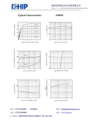
NPN SS8050SS8050 TRANSISTOR (NPN) SOT-23 FEATURES Complimentary to SS8550 1BASE 2EMITTER 3COLLECTOR MARKING: Y1 MAXIMUM RATINGS (TA=25 unless otherwise noted) Symbol Parameter Value Units VCBO Collector-Base Voltage 40 V VCEO Collector-Emitter Voltage 25 V VEBO Emitter-Base Voltage 5 V IC Collector Cu
s8050.pdf


S8050SOT-23 Plastic-Encapsulate TransistorsTRANSISTOR (NPN) FEATURES Complimentary to S8550 Collector Current: IC=0.5A MARKING: J3Y MAXIMUM RATINGS (Ta=25 unless otherwise noted) Symbol Parameter Value Unit V Collector-Base Voltage 40 V CBOSOT-23 V Collector-Emitter Voltage 25 V CEOVEBO Emitter-Base Voltage 5 V IC Collector Current 500 mA 1. BASE 2. EMITT
ss8050t23.pdf


SS8050T23NPN Transistor ROHS FEATURE NPN Transistor Collector Current: IC=1.5A MARKING:Y1SOT-23Absolute maximum ratings (Ta=25 unless otherwise noted)Symbol Parameter Value UnitsVCBO Collector-Base Voltage 40 VVCEO Collector-Emitter Voltage 25 VVEBO Emitter-Base Voltage 5 VIC Collector Current -Continuous 1.5 APC Collector Power Dissipation 0.3 W Tj
s8050.pdf


MOT S8050NPN-TRANSISTORNPN NPN Plastic-Encapsulate Transistors SMDHigh breakdown voltageS8050Low collector-emitter saturation voltageTransistor Polarity: NPNTransistor pinout: BECMMBT8050LT1SOT-23 PackageMarking Code: J3YInner circuit 8050 Series
ss8050.pdf


SS8050 MOTNPN TRANSISTOR NPN NPN High Voltage Transistor SMD SS8050 NPN, BEC Transistor Polarity: NPN General Purpose Transistors Transistor pinout: BEC SOT-23 Package Marking Code: Y1 hFE: 100~200, 200~300 Ldeal for Medium Power Amplification and Switching Inner circuit
mmbtss8050l mmbtss8050h mmbtss8050j.pdf


MMBTSS8050NPN Silicon General Purpose Transistors FeaturesSOT23 High current capacity in compact package IC = 1.5A. Epitaxial planar type Pb-Free package is availableMechanical data Epoxy:UL94-V0 rated flame retardant(B)(C) Case : Molded plastic, SOT-23(A) Terminals : Solder plated, solderable perMIL-STD-750, Method 20260.063 (1.60)0.027 (0.67)
s8050l s8050h s8050j.pdf


S8050 Features Complimentary to S8550 Collector Current: IC=0.5A SOT-23Marking Code:J3YADim Min MaxCA0.37 0.51B C B1.20 1.40C2.30 2.50TOP VIEWB ED0.89 1.03DEGE0.45 0.60G1.78 2.05H H2.80 3.00JMAXIMUM RATINGS (Ta=25 unless otherwise noted) 0.013 0.10KK0.903 1.10SymbolParameter
ss8050l ss8050h ss8050j.pdf


SS8050 Features Complimentary to SS8550 Collector Current: IC=1.5A SOT-23AMarking Code:Y 1Dim Min MaxCA0.37 0.51B C B1.20 1.40C2.30 2.50TOP VIEWB ED0.89 1.03DEGE0.45 0.60G1.78 2.05H H2.80 3.00 J0.013 0.10KMAXIMUM RATINGS (Ta=25 unless otherwise noted) K0.903 1.10JL0.45 0.61
s8050b s8050c s8050d.pdf


Jiangsu Weida Semiconductor Co., Ltd.S8050NPN General Purpose TransistorsTO-921. EMITTER122. BASE33. COLLECTORABSOLUTE MAXIMUM RATINGS(Ta=25 C)Rating Symbol Value UnitVCEOCollector-Emitter Voltage 25 VdcVCBOCollector-Base Voltage 40 VdcVEBOEmitter-Base VOltage 5.0 VdcCollector Current IC 500 mAdcPDTotal Device Dissipation T =25 C 0.625 WAJunction Te
ss8050b ss8050c ss8050d ss8050e.pdf


Jiangsu Weida Semiconductor Co., Ltd.SS8050NPN General Purpose TransistorsTO-92P b Lead(Pb)-Free1. EMITTER122. BASE33. COLLECTORMAXIMUM RATINGS(TA=25C unless otherwise noted)Rating Symbol Value UnitVCBO40Collector-Base Voltage VCollector-Emitter Voltage VCEO 25VVEBOEmitter-Base Voltage 5 VCollector Current-ContinuousIC A1.5Total Device Dissipation
Datasheet: 2N3200 , 2N3201 , 2N3202 , 2N3203 , 2N3204 , 2N3205 , 2N3206 , 2N3207 , TIP31 , 2N3209 , 2N3209AQF , 2N3209CSM , 2N3209DCSM , 2N3209L , 2N321 , 2N3210 , 2N3211 .
History: BC214


